An Energy-Efficient Area-Efficient DAC for SAR ADC
胡云峰,易子川,何志红(. 电子科技大学中山学院,电子薄膜与集成器件国家重点实验室中山分实验室,中国 中山 528402;2. 深圳市国华光电科技有限公司,中国 深圳 580)
An Energy-Efficient Area-Efficient DAC for SAR ADC
Digital-to-analogue(DAC) is one of the important energy consumption sources of successive approximation register analogue-to-digital converter (SAR ADC). In order to reduce the energy consumption of DAC, an energy-efficient DAC structure which consists of four sub-DACs is proposed. By using extra-step technique during the DAC switching procedure, the two sub-DACs in the same side will combine to generate the required output of DAC. Moreover, Sub-DAC combination will reduce the required number of unit capacitors and decrease the energy consumption. Simulation results show that, in comparison with the traditional DAC structure, the proposed structure can decrease the energy consumption by 99.89% and reduce the number of unit capacitors by 96.88%.
energy-efficient; area-efficient; SAR ADC; sub-DAC combination; extra-step
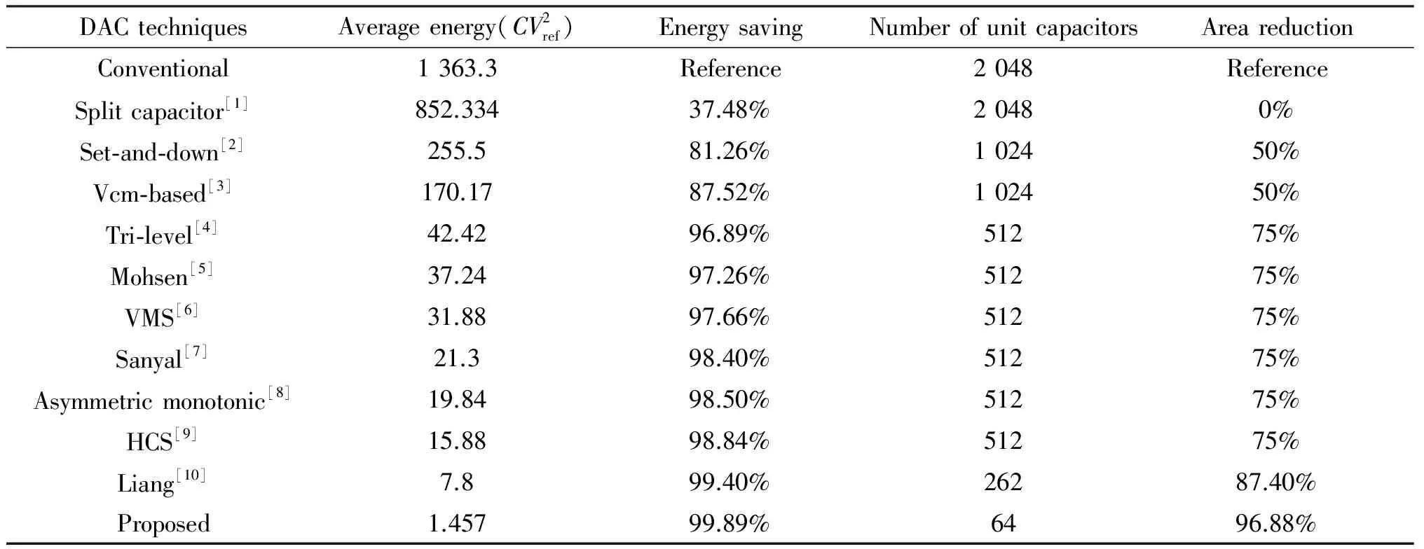
In successive approximation register (SAR) analogue-to-digital converters (ADCs), DAC consumes a significant part of the total power consumption[1]. Recently, several energy-efficient techniques have been developed to improve the power efficiency of DAC[1-10]. Compared to conventional technique, Split capacitor [1], Set-and-down[2], Vcm-based[3], Tri-level[4], Mohsen[5], VMS[6], Sanyal[7], Asymmetric monotonic[8], HCS[9], Liang[10]reduced the energy consumption by 37.48%, 81.26%, 87.52%, 96.89%, 97.26%, 97.66%, 98.40%, 98.50%, 98.84% and 99.40%, respectively. In this paper, a more energy-efficient and area-efficient DAC is presented which can achieve the reduction of 99.89% in the energy consumption of the DAC.
1 The proposed DAC
1.1 The structure of the proposed DAC
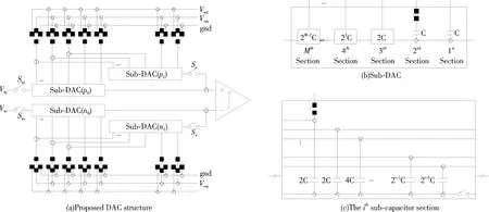
The structure of the proposed DAC for SAR ADC is shown in Fig.1. The DAC consists of four sub-DACs, sub-DAC(p0), sub-DAC(p1), sub-DAC(n0) and sub-DAC(n1), with the first two combined into one sub-DAC combination and the latter two into another one. Each sub-DAC hasM(M=N/2, ifNis even;M=(N+1)/2, ifNis odd) sub-capacitor sections and the number in each box is the total capacitance of the sub-capacitor section. All the top plates of the sub-capacitor sections connecting serially through additional switches join to sampling port, and their bottom plates connect serially.

Fig.1 The structure of the proposed DAC for SAR ADC
1.2 The application of extra-step in sub-DAC combination
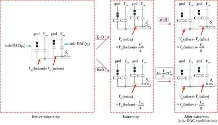
The main idea of this paper stems from the method of using an extra-step to generate an extra voltage on the DAC, and combining sub-DACs (as shown in Fig.1.) to get a finer voltage. It can save more energy and reduce more areas for DAC than that by conventional techniques.

Fig.2 The application of extra-step in sub-DAC combination
As shown in Fig.2, in “Before extra-step”, the sub-DAC(p0) and sub-DAC(p1) have the same voltage as they use the same reference voltage. In “Extra-step”, the voltage of sub-DAC(p1) increases byVref/4 through a shift in the reference voltage of the second capacitor from gnd toVcm; the voltage of sub-DAC(p1) decreases byVref/4 through a shift in the reference voltage of the first capacitor fromVcmto gnd. In “After extra-step”, the switches between the second capacitor and reference voltage in both of the sub-DAC(p0) and sub-DAC(p1) are opened, while the switchSpbetween sub-DAC(p0) and sub-DAC(p1) is closed. In this way, a finer voltage of sub-DAC(p0) and sub-DAC(p1),Vref/8 or-Vref/8, is achieved through the application of extra-step technique.
1.3 Operation of the proposed DAC
Before extra-step, The firstM+1 bits are generated by using only the sub-DAC(p0) and the sub-DAC(n0), while switchesSpandSnare opened. During the extra-step, an extra voltage is produced through a shift in the reference voltage of the first or the second capacitor in sub-DAC(p1) or the sub-DAC(n1),according to the output in the (M+1)thcomparison. After extra-step, the lastN-M-1 bits are generated by combining sub-DAC(p1) with sub-DAC(p0) or combining sub-DAC(n1) with sub-DAC(n0).
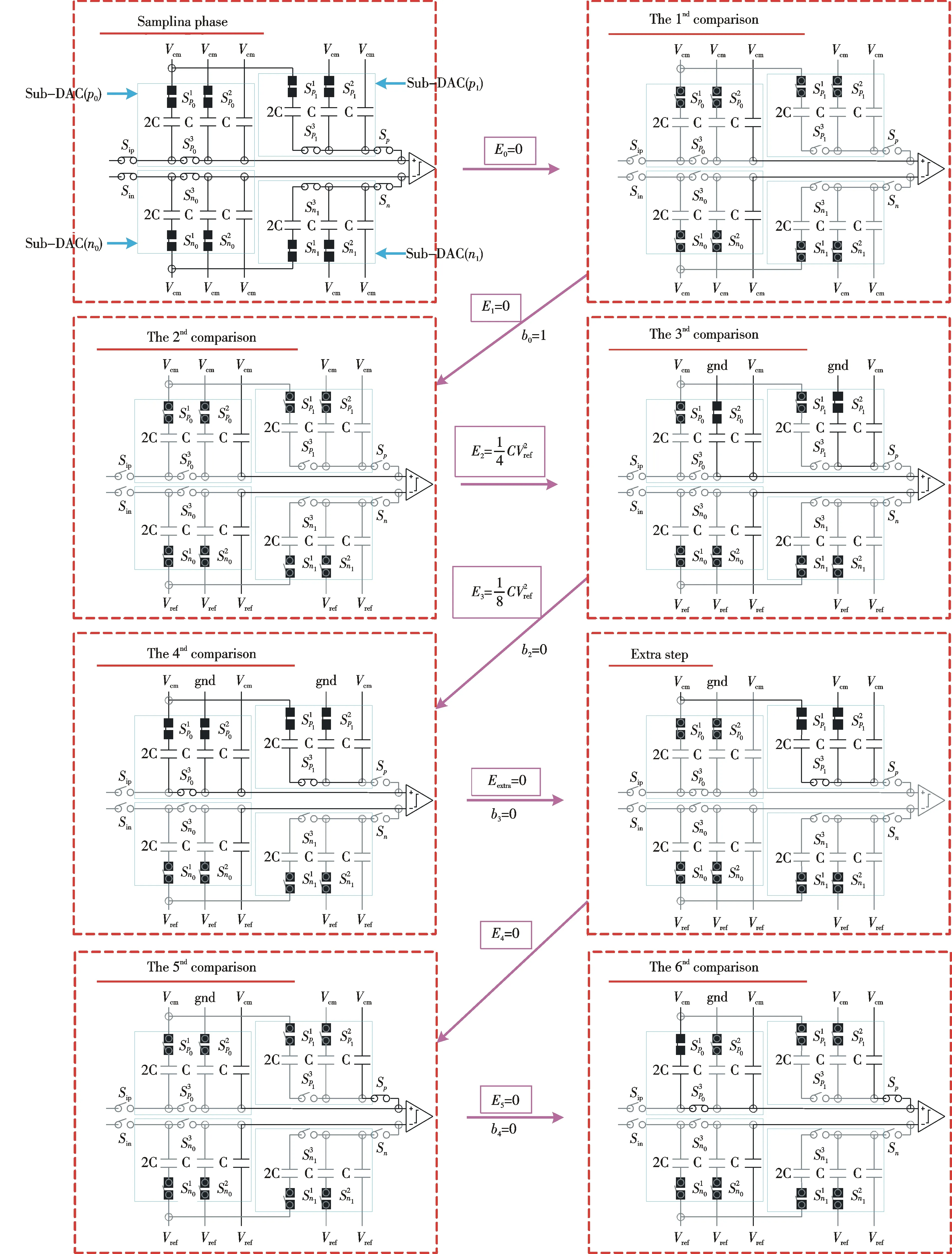
For simplicity, the proposed switching mechanism is described by using a 6-bit SAR ADC. Let the output be the digital word (b0,b1,b2,b3,b4,b5) =110 011. The steps of the conversion process are illustrated in Fig.3.

Fig.3 Operation of the proposed SAR ADC with the digital word being 110 011
Initially, in the sampling phase, all switches are closed, and the reference voltage of all capacitors is set toVcm. The input voltage is sampled onto the top plates of capacitors.
In the 1stcomparison, all switches are opened, the output voltage of the capacitor array are found to be
(1)
The comparator compares the sampling signals(VipandVin) and getb0.
In the 2ndcomparison, sinceb0is 1, the reference voltage of capacitors in the sub-DAC(n0andn1) is changed fromVcmtoVref, and the output voltages are found to be
(2)
The comparator comparesVp0(2) withVn0(2), and getb1.
(3)
The comparator comparesVp0(3) withVn0(3), and getb2.
(4)
The comparator comparesVp0(4) withVn0(4), and getb3.
During the extra step, sinceb3is 0, the reference voltage of the second sub-capacitor section in the sub-DAC(p1) is changed from gnd toVcm, and the output voltages are found to be
(5)

(6)
The comparator comparesVp0(5) withVn0(5), and getb4.

(7)
The comparator comparesVp0(6) withVn0(6), and getb5.
The energy of DAC consumed[1]at each step is as follows.
(8)
WhereE0,E1,E2,E3,E4andE5represent the energy of DAC required to determineb0,b1,b2,b3,b4andb5, respectively.Eextrarepresent the energy consumption in extra-step.
2 Simulation results

Fig.4 DAC energy against output code


Tab.1 Comparison of DAC techniques for 10-bit SAR ADC
3 Conclusion
A novel energy-efficient and area-efficient DAC for SAR ADC, with an energy savings of 99.89% and an area reduction of 96.88% compared to the conventional technique, is presented. Thanks to the using of extra-step in sub-DACs combinations, the proposed DAC achieves lower energy and smaller area compared to the published DACs.
[1] GINSBURG B P, CHANDRAKASAN A P. An energy-efficient charge recycling approach for a SAR converter with capacitive DAC[C]. Proceedings of 2005 IEEE International Symposium on Circuits and Systems, Kobe, Japan: ISCAS, 2005:184-187.
[2] LIU C C, CHANG S J, HUANG G Y,etal. A 10-bit 50-MS/s SAR ADC with a monotonic capacitor switching procedure[J]. IEEE J Solid-State Circ, 2010,45(4):731-740.
[3] ZHU Y, CHAN CH, CHIO UF,etal. A 10-bit 100-MS/s reference-free SAR ADC in 90 nm CMOS[J]. IEEE J Solid-State Circ, 2010,45(6):1111-1121.
[4] YUAN C, LAM Y. Low-energy and area-efficient tri-level switching scheme for SAR ADC[J]. Elect Lett, 2012,48(9):482-483.
[5] SHAHMOHAMMADI M, ASHTIANI S J, KAMAREI M. Energy and area-efficient tri-level switching procedure based on half of the reference voltage for SAR ADC[J]. IEICE Elect Exp, 2012,9(17):1397-1401.
[6] ZHU Z M, YU X, SONG X L. VCM-based monotonic capacitor switching scheme for SAR ADC[J]. Elect Lett, 2013,49(5):327-329.
[7] SANYAL A, SUN N. SAR ADC architecture with 98% reduction in switching energy over conventional scheme[J]. Elect Lett, 2013,49(4):248-250.
[8] SONG H, LEE M. Asymmetric monotonic switching scheme for energy-efficient SAR ADCs[J]. IEICE Elect Exp, 2014,11(12):20140345.
[9] XIE L B, WEN G J, LIU J X,etal. Energy-efficient hybrid capacitor switching scheme for SAR ADC[J]. Elect Lett, 2014,50(1):22-23.
[10] LIANG Y, ZHU Z M, LIU J,etal. Strategy for SAR ADC with 87.5% area saving and 99.4% switching energy reduction over conventional approach[J]. IEICE Elect Exp, 2015,12(8):20150058.
(编辑 CXM)
2017-03-09
国家自然科学基金资助项目(60976026);广东省科技计划资助项目(00760211330304099,2014B090914004,2016B090918083);广东省引进创新科研团队计划资助项目(2013C102);深圳市科技计划资助项目(GQYCZZ20150721150406);中山市科技计划资助项目(2016B2146)
HU Yun-feng1, YI Zi-chuan1,2, HE Zhi-hong1
(1.State Key Laboratory of Electronic Thin Films and Integrated Devices, Zhongshan Branch, Zhongshan Institute, University of Electronic Science and Technology of China, Zhongshan 528402, China; 2. Shenzhen Guohua Optoelectronic Technology Co., Ltd., Shenzhen 518110, China)
TN453
A
1000-2537(2017)03-0058-06
数模转换器(DAC)是逐次逼近型模数转换器(SAR ADC)能耗的重要来源之一. 为了降低DAC能耗,提出一种高能效高面效DAC结构,该结构包含四个子DAC. 在DAC转换过程中,通过采用附加步技术,使同边的两个子DAC结合产生所需要的DAC输出电压. 而且,子DAC结合可使所需的单位电容数量减少,能耗降低. 仿真结果表明,相比于传统的DAC结构,文中提出的DAC结构可降低99.89%的能耗,节省96.875%的单位电容数量.
高能效;高面效;逐次逼近型模数转换器;子DAC结合;附加步
10.7612/j.issn.1000-2537.2017.03.011
一种用于SAR ADC的高能效高面效DAC
胡云峰1*,易子川1,2,何志红1
(1. 电子科技大学中山学院,电子薄膜与集成器件国家重点实验室中山分实验室,中国 中山 528402;2. 深圳市国华光电科技有限公司,中国 深圳 518110)
*通讯作者,E-mail:shanhuyf@163.com

