基于硅过渡层纳米金刚石膜/GaN复合膜系的制备
刘金龙, 田寒梅, 陈良贤, 魏俊俊, 黑立富, 李成明
(北京科技大学 新材料技术研究院,北京100083)
基于硅过渡层纳米金刚石膜/GaN复合膜系的制备
刘金龙, 田寒梅, 陈良贤, 魏俊俊, 黑立富, 李成明
(北京科技大学 新材料技术研究院,北京100083)
本文研发了一种简便有效的在GaN半导体衬底上直接生长纳米金刚石膜的方法。研究发现,直接将GaN衬底暴露于氢等离子体中5 min即发生分解,且随着温度从560 ℃升高至680 ℃,这种分解反应愈加剧烈,很难在GaN衬底上直接形成结合力良好的纳米金刚石膜。通过在GaN衬底上镀制几纳米厚的硅过渡层,在富氢金刚石生长环境下,抑制了GaN衬底的分解,同时在GaN衬底上沉积了约2 μm厚的纳米金刚石膜。硅过渡层厚度是决定纳米金刚石与GaN衬底结合力的主要因素。当硅过渡层厚度为10 nm时,纳米金刚石膜与GaN衬底呈现出大于10 N的结合力,可能与硅过渡层在金刚石生长过程中向SiC过渡层转变有关。
氮化镓;硅过渡层;纳米金刚石膜;直接生长;分解
1 Introduction
Gallium nitride (GaN) has been widely applied in electronic and optoelectronic devices, owing to their unique electrical properties such as large bandgap (3.4 eV), high breakdown electrical field (3×10⁶V·cm-1) and extremely high saturation velocity (1.5×107cm·s-1), and high electron mobility in AlGaN/GaN heterostructures (2 019 cm2/V·s)[1-3]. However, the low thermal conductivity of GaN and the high thermal boundary resistances (TBRs) at interfaces between GaN and substrates such as Si and Al2O3in composites impede efficient heat dissipation from the heated regions in device[4,5]. It has been reported that the working temperature of AlGaN/GaN heterostructure field-effect transistors (HFETs) is currently on the order of 180 ℃, which may increase with growing current densities[6]. This self-heating severely limits the further development of GaN based high power devices. SiC is one of the most suitable heat sink materials for these devices with a high thermal conductivity of 400 W/m·K and a small lattice mismatch of 3%. Currently, a maximum output power density of 30 W/mm for AlGaN/GaN high electron mobility transistor (HEMT) on SiC was achieved[7,8].
Diamond, with the highest thermal conductivity of 2 200 W/m·K, has been speculated to be the optimal substrate for GaN based devices[9-11]. It has been obtained that the maximum channel current of AlGaN/GaN HEMT on diamond is nearly twice as high as that on SiC, and the corresponding channel temperature is 100 ℃ lower based on the simulation than that on SiC[12]. However, whether GaN on the diamond, or diamond on GaN is hard to prepare, because there is a large thermal expansion coefficient difference and lattice mismatch between them. For the former, the GaN heteroepitaxy growth on a single crystalline or polycrystalline diamond is difficult to control[2,13], although GaN based devices on silicon-on-diamond (SOD) has been reported by SP3 company[14]. While for the latter, a high substrate temperature for the diamond film deposition (≈800 ℃) and H-rich environment may lead to a GaN degradation due to the hydrogen plasma etching and GaN decomposition[15,16]. Thus, some approaches have been explored to integrate diamond with GaN through some interlayers such as AlN and Si3N4dielectric adhesive layers[15,17,18]. However, the thick interlayer may become a thermal barrier to impede the heat dissipation.
In this paper, we presented an approach to achieve a direct deposition of the nano-diamond film on GaN by incorporating a thin Si buffer layer. The buffer layer thickness was just several nanometers, which prevented the GaN substrate from hydrogen etching. The thickness of nano-diamond films deposited could be varied from several hundred nanometers to several micrometers, which will effectively improve the thermal conductivity of GaN based devices.
2 Experimental
A commercial GaN/sapphire composite with a GaN thickness of about 25 μm was used as the substrate. Before nano-diamond film deposition, the substrate was overgrown with a Si buffer layer with several nanometers-thick using the RF magnetron sputtering. In order to improve the adhesion of the Si layer on GaN, the GaN/sapphire composite was firstly bombarded by the Ar+ion with 1 250 eV energy for 15 min. And then the Si buffer layers with thickness of 5, 10, 20 and 40 nm were deposited on the GaN/sapphire substrates by controlling the deposition time. After the seeding treatment using a suspension of absolute alcohol mixed with 5 nm diamond powders, hydrogen rich plasma environment consisting of CH4/H2(6/94) was used to prepare the nano-diamond films in a 5 kW microwave (MW) reactor chamber. The deposition parameters are listed in Table 1. The substrate temperature was kept at 680 ℃ through adjusting the microwave power and pressure. At this temperature, it is considered that loss of nitrogen (N) from GaN won’t happen and hydrogen rich environment can’t result in the poor-quality of diamond. The nano-diamond films on GaN/sapphire composites were prepared after deposition for 3 h. The surface morphology of the GaN/sapphire with and without Si buffer layers after nano-diamond film deposition was observed by SEM (QUANTA FEG 450). The surface and cross section of diamond/GaN/sapphire composite was characterized by Raman spectroscopy using an excitation wavelength of 514 nm. The adhesion force between nano-diamond and GaN/sapphire substrate was evaluated by a micro scratch tester (WS-2005).

Table 1 Deposition parameters of nano-diamond films on GaN by MWCVD.
3 Results and discussion
3.1 Surface morphology of GaN exposed to hydrogen plasma and after direct growth of diamond film
Before nano-diamond growth on the GaN/sapphire composite, the surface morphology of GaN exposed to the hydrogen plasma for 5 min is firstly observed and shown in Fig.1. It can be seen that some pin holes appear on the GaN surface, which spread and connect with each other in the plane direction. Finally, the whole GaN film decomposes with a substrate temperature increase from 560 to 680 ℃. According to the model reported by Yeh et al[19], the etching reaction on GaN in the hydrogen-rich environment started from the dislocation sites, and at high temperature a formation of Ga droplet would accelerate the GaN decomposition, which can be obviously found in Fig.1(d) in our situation. It can be also seen that the GaN surface is almost unchanged after the exposure to hydrogen plasma at 560 ℃ in Fig.1(a). We have tried to deposit the nano-diamond films on the GaN/sapphire composites directly without the Si buffer layer at 560 and 680 ℃. However, it is hard to form diamond film at 560 ℃, while it shows a weak adhesion between nano-diamond film and the GaN/sapphire composite at 680 ℃, although the dense nano-diamond film can be formed in the latter case as shown in Fig.2. That’s because that GaN will decompose at 680 ℃ by hydrogen plasma etching due to the high deposition temperature at the early stage of nano-diamond film deposition, as shown in Fig.2(a).
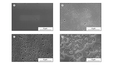
Fig. 1 Morphologies of GaN exposed to hydrogen plasma at (a) 560 ℃, (b) 600 ℃,(c) 640 ℃ and (d) 680 ℃ for 5 min.

Fig. 2 Surface morphologies of (a) GaN and (b) nano-diamond film after diamond film deposition at 680 ℃.
As the carbon source is added and chemical species containing carbon reaches the GaN surface, some amorphous carbon will form preferentially due to lack of favorable nucleation condition for the diamond, and diamond film is formed and grown by transformation of amorphous carbon layer, which is indicated in Fig.2(b). The loose amorphous carbon layer results in a weak adhesion between nano-diamond film and GaN substrate.
3.2 Characterization of GaN with nano-diamond film by using the Si buffer layer
Morphology of nano-diamond films on the GaN/sapphire substrates with different thicknesses of Si buffer layers is shown in Fig.3. It can be seen that the diamond films are composed of many clusters on the GaN substrate, which shows the typical feature of nano-diamond films. The sample with a 40 nm-thick Si layer is not shown here because the diamond film was peeled off immediately when the microwave generator was shut down. Correspondingly, Raman spectra of nano-diamond films on the GaN/sapphire substrates with different thicknesses of Si buffer layers are shown in Fig.3(d). For the sample with the 5 nm Si layer, it consists of peaks at 1 177, 1 334, 1 477 and 1 580 cm-1. As it is known that the peaks at 1 177 and 1 477 cm-1can be attributed to nano-diamond, which are contributed by the tans-polyacetylene on grain boundary or disordered sp3carbon. The peak at 1 334 cm-1is typical of diamond while that at 1 580 cm-1peak is excited by the G-mode vibration of sp2amorphous carbon. As the thickness of the Si buffer layer increases, the peak at 1 477 cm-1disappears and the intensity of the peak at 1 334 cm-1increases, which indicates that the diamond content with a sp3structure increases. We can’t find the obvious characteristic peaks of GaN for all three samples. This is because the diamond film is thick enough to exceed the detect limit in the depth direction (generally about 1 μm) for Raman spectroscopy.
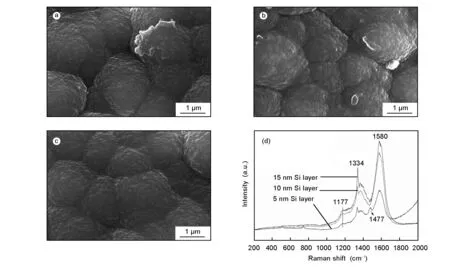
Fig. 3 Morphologies and Raman spectra of nano-diamond films on the GaN/sapphire substrates with different thicknesses of Si buffer layers. (a-c) Surface morphologies and (d) Raman spectra of samples with 5, 10 and 20 nm thick Si layers.
In order to determine whether the GaN substrate was decomposed directly, the cross sectional morphology of nano-diamond films on the GaN/sapphire substrate with a 5 nm Si buffer layer was characterized, which is shown in Fig. 4. The GaN film with a thickness of 24.28 μm can be observed clearly, on top which there is a thin nano-diamond film with a thickness of about 2 μm. The edge of the top surface is neat, which suggests that the GaN doesn’t almost decompose under the H-rich plasma environment with a Si buffer layer. Further, the components of the cross section of GaN were detected by energy dispersive spectrum (EDS), as shown in Fig.4(b). It can be found that no other impurities can be observed besides the N and Ga elements. The atom ratio of Ga and N is near 1, which indicates that the GaN is intact under the shield of a thin Si layer during the H-rich plasma etching in the diamond growth process.
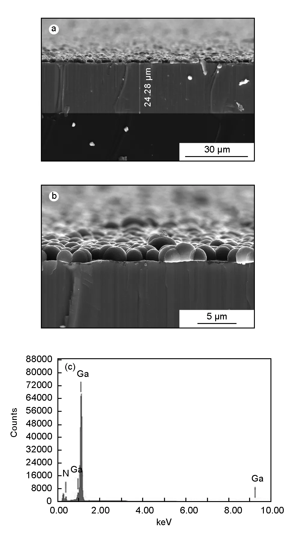
Fig. 4 (a, b) Cross sectional morphology and (c) EDS of nano-diamond films on the GaN/sapphire substrate with the 5 nm Si buffer layer.
3.3 Adhesion evaluation between nano-diamond film and the GaN substrate In order to evaluate the adhesion of nano-diamond film on GaN, micro scratch test was conducted. Fig.5 shows the typical scratch appearance of nano-diamond film on the GaN.
As the pressure of diamond intender increases, just the trace rubbed between nano-diamond film and diamond intender is left on the nano-diamond film surface at the early stage, as shown in Fig.5(a), then the nano-diamond film is ground and peeled off as shown in Fig.5(b) and Fig.5(c), and finally the GaN is exposed as shown in Fig.5(d). It is noticed that it doesn’t show the GaN substrate directly in Fig.5(c) after the diamond film starts to spall, indicating that there is a transition layer between the nano-diamond film and the GaN substrate. We can evaluate the adhesion from the sound signal change for the brittle nano-diamond film on the GaN substrate as shown in Fig.6. From the sound signal, it can be found that nano-diamond film on the GaN has a low adhesion for the samples with the 5 and 20 nm thick Si buffer layers. While for the sample with the 10 nm-thick Si buffer layer, it shows a high adhesion beyond 10 N. It seems strange that a several nanometer thick difference of the Si interlayer leads to a large difference of adhesion. In fact, when the buffer layer thickness reaches 40 nm, the nano-diamond film is easy to be broken away from the GaN substrate. While for the sample with a thickness of 5 nm, no obvious zone of diamond grinding is observed.
3.4 Discussion
Decomposition of the GaN substrate during nano-diamond film growth has been effectively suppressed by using a thin Si layer as buffer deposited before the diamond growth. After nano-diamond film deposition, the thickness of GaN was almost unchangeable. More importantly, a good adhesive between the micrometer thick nano-diamond film and the GaN substrate was obtained. In general, nucleation of diamond only happens on carbide forming materials such as some refractory metals or Si (except for growth on Ir)[20], so there is no enough driving force for a direct nucleation of diamond films on the GaN substrate. A direct growth of diamond film on the GaN substrate is thermodynamically favorable by adding some carbide forming element material, such as W[11]or Si. However, due to a large mismatch stress (about 13%) and thermal expansion coefficient difference between diamond film (1.0×10⁻⁶/℃) and GaN (5.59×10⁻⁶/℃), a direct bonding between them seems impossible, especially as the thickness of diamond film increases, the mismatch stress becomes large enough to separate the diamond film from the GaN substrate. In our situation, the thin Si buffer layer several-nanometer thick may convert to SiC during the diamond nucleation although the lattice constant of Si is larger than diamond and GaN. It is known that there is a small lattice mismatch of 3% between SiC and GaN. Meanwhile, SiC and diamond film can form strong chemical bonding. Therefore, a tight adhesion is expected to be achieved between diamond film and the GaN substrate. It is worth noting that the thickness of Si buffer layer is an important factor that determines the adhesion between diamond film and the GaN substrate. If it is thicker than 20 nm, the Si layer can’t transform to SiC completely and the interface bonding between GaN and the Si buffer layer becomes weak. While if it is too thin like 5 nm, it may not relax the large stress between diamond film and the GaN substrate. Hence, a 10 nm-thick Si buffer layer is considered to be optimum to improve the adhesion between nano-diamond film and the GaN substrate owing to their strong bond. Meanwhile it can be speculated that a 2 μm-thick nano-diamond film could provide large heat sinking capacity for high power GaN based electronic devices according to the results reported in Ref.[11].
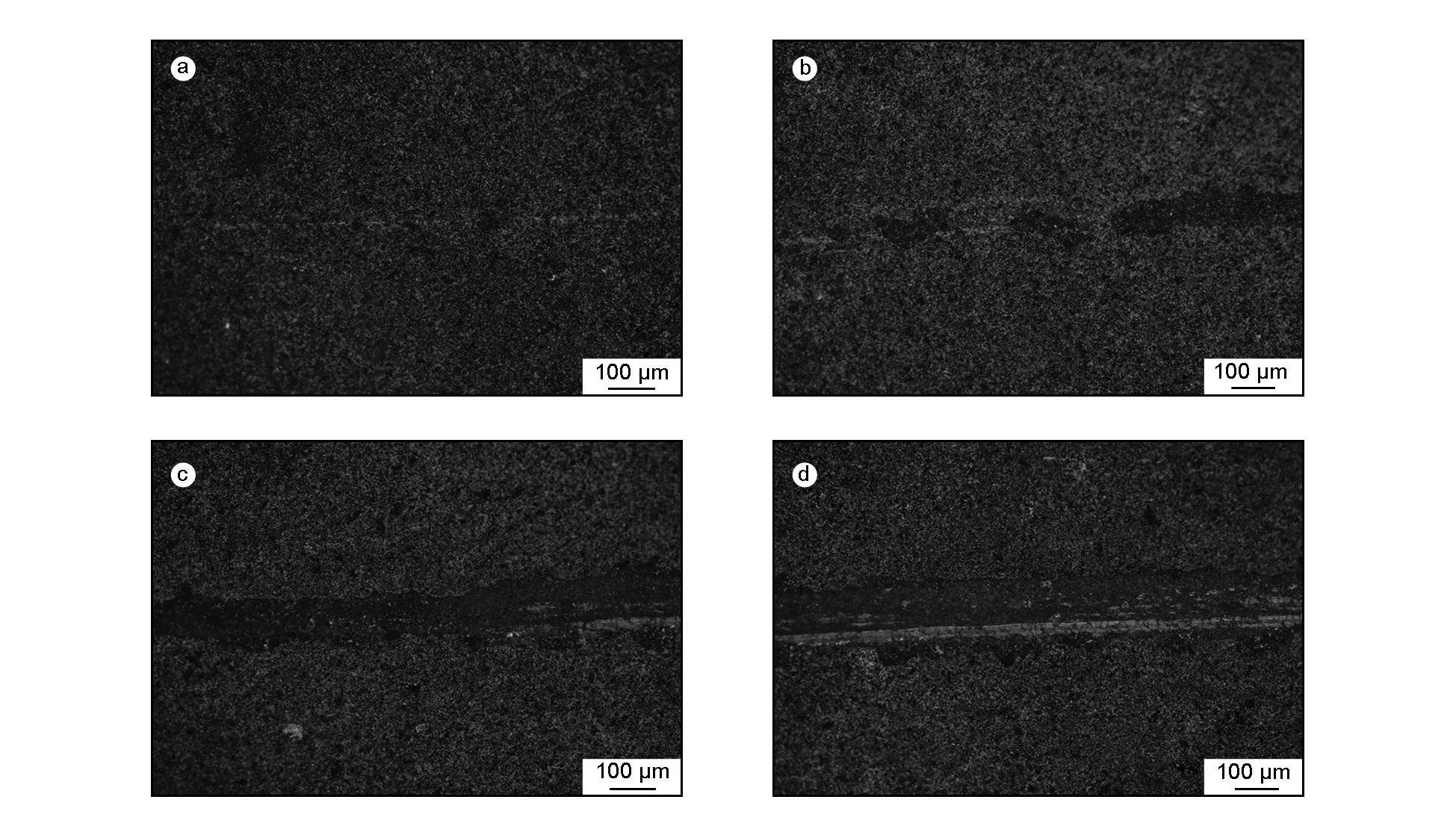
Fig. 5 The typical scratch appearance of nano-diamond film on the GaN/sapphire with Si buffer layers.(a) The trace rubbed between nano-diamond film and diamond intender at the early stage; (b) the nano-diamond film begins to peel off;(c) the transition layer between nano-diamond film and GaN and (d) the exposed GaN substrate.
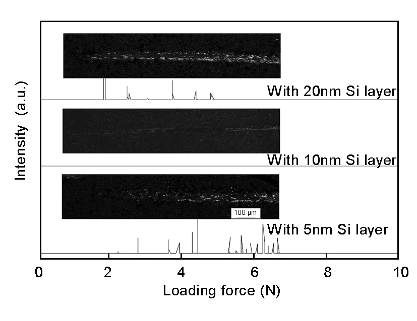
Fig. 6 The sound signal and the corresponding scratch morphology of nano-diamond film on the GaN/sapphire with different thicknesses of the Si buffer layers after the scratch test.
4 Conclusions
When exposed to the hydrogen plasma for 5 min, the GaN substrate decomposed apparently with a substrate temperature increase from 560 to 680 ℃ and nano-diamond film cannot be grown on the GaN substrate adhesively without the aid of a Si buffer layer. A 2 μm-thick nano-diamond film was directly grown on the GaN/sapphire substrate by using a several nanometer thick Si buffer layer. The cross-sectional morphology and EDS of nano-diamond film on the GaN/sapphire substrate demonstrate that decomposition of GaN was significantly suppressed during diamond growth under the H-rich plasma environment in the presence of a Si buffer layer. It is found that the adhesion force between nano-diamond film and the GaN/sapphire substrate is larger than 10 N when a 10 nm-thick Si layer is present, which is attributed to a complete conversion of the Si layer to a silicon carbide (SiC) transition layer.
[1] Gelmont B, Kim K, Shur M. Monte carlo simulation of electron transport in gallium nitride[J]. Journal of Applied Physics, 1993, 74(3): 1818-1821.
[2] Zhang D, Bian J M, Qin F W, et al. Highly c-axis oriented GaN films grown on free-standing diamond substrates for high-power devices[J]. Materials Research Bulletin, 2011, 46(10): 1582-1585.
[3] Gaska R, Yang J W, Osinsky A, et al. Electron transport in AlGaN heterostructures grown on 6H-SiC substrates[J]. Applied Physics Letters, 1998, 72(6): 707-709.
[4] Sadi T, Kelsal R W, Pilgrim N J. Investigation of self-heating effects in submicrometer GaN/AlGaN HEMTs using an electrothermal Monte Carlo method[J]. IEEE Transactions on Electron Devices, 2006, 53(12): 2892-2900.
[5] Trew R J, Green D S, Shealy J B. AlGaN/GaN HFET reliability[J]. IEEE Microwave Magazine, 2009, 10(4): 116-127.
[6] Kuball M, Hayes J M, Uren M J, et al. Measurement of temperature in active high-power AlGaN/GaN HFETs using Raman spectroscopy[J]. IEEE Eletron Device Letters, 2002, 23(1): 7-9.
[7] Felbinger J G, Chandra M V S, Sun Y J, et al. Comparison of GaN HEMTs on diamond and SiC substrates[J]. IEEE Eletron Device Letters, 2007, 28(11): 948-950.
[8] Wu Y F, Saxler A, Moore M, et al. 30W/mm GaN HEMTs by field plate optimization[J]. IEEE Electron Device Letters, 2004, 25(3): 117-119.
[9] Govindaraju N, Singh R N. Processing of nanocrystalline diamond thin films for thermal manage-ment of wide-bandgap semiconductor power electronics[J]. Materials Science and Engineering: B, 2011, 176(14): 1058-1072.
[10] Diduck Q, Felbinger J, Eastman L F, et al. Frequency performance enhancement of AlGaN/GaN HEMTs on diamond[J]. Electron Letters, 2009, 45(14): 758-759.
[11] Goyal V, Sumant A V, Teweldebrhan D, et al. Direct low-temperature integration of nano- crystalline diamond with GaN substrates for improved thermal management of high-power electronics[J]. Advanced Functional Materials, 2012, 22(7): 1525-1530.
[12] Joshi B C, Dhanavantri C, Kumar D. Sapphire, SiC, AlN, Si and diamond-substrate material for GaN HEMT and LED[J]. Journal of Optoelectronics and Advanced Materials, 2009, 11(8): 1111-1116.
[13] Zhang D, Bai Y Z, Qin F W, et al. Preparation and characteristics of GaN films on freestanding CVD thick diamond films[J]. Chinese Physics Letters, 2010, 27(1): 018102-018102-4.
[14] Zimmer J W, Chandler G. Advances in large diameter GaN on diamond substrates [C]. CS Mantech Conference, Chicago, USA, April 14-17, 2008.
[15] Zou Y S, Yang Y, Chong Y M, et al. Chemical vapor deposition of diamond films on patterned GaN substrates via a thin silicon nitride protective layer[J]. Crystal Growth and Design, 2008, 8(5): 1770-1773.
[16] May P W, Tsai H Y, Wang W N, et al. Deposition of CVD diamond onto GaN[J]. Diamond and Related Materials, 2006, 15(4-8): 526-530.
[17] Francis D, Faili F, Babi D, et al. Formation and characterization of 4-inch GaN-on-diamond substrates[J]. Diamond and Related Materials, 2010, 19(2-3): 229-233.
[18] Hageman P R, Schermer J J, Larsen P K. GaN growth on single-crystal diamond substrate by metalorganic chemical vapour deposition and hydride vapour deposition[J]. Thin Solid Film, 2003, 443(1-2): 9-13.
[19] Yeh Y H, Chen K M, Wu Y H, et al. Hydrogen etching of GaN and its application to produce free-standing GaN thick films[J]. Journal of Crystal Growth, 2011, 333(1): 16-19.
[20] Alomari M, Dipalo M, Rossi S, et al. Diamond overgrown InAlN/GaN HEMT [J]. Diamond and Related Materials, 2011, 20(4): 604-608.
Preparation of nano-diamond films on GaN with a Si buffer layer
LIU Jin-long, TIAN Han-mei, CHEN Liang-xian, WEI Jun-jun, HEI Li-fu, LI Cheng-ming
(InstituteforAdvancedMaterialsandTechnology,UniversityofScienceandTechnologyBeijing,Beijing100083,China)
Gallium nitride (GaN) has been widely used in electronic and optoelectronic devices because of its unique electrical properties. However, its low thermal conductivity and the high thermal boundary resistance at the interface between GaN and substrates such as Si and Al2O3prevent efficient heat dissipation from the heated regions, which limits the further development of GaN-based high power devices. Diamond, with the highest thermal conductivity, has been considered to be one of the most promising heat sink materials. However, it is hard to prepare a diamond film on a GaN substrate because there is a high thermal expansion coefficient difference and also a large lattice mismatch between them. An approach to prepare a nano-diamond film on a GaN substrate by incorporating a Si buffer layer has been proposed. A GaN substrate decomposes significantly from 560 to 680 ℃ when exposed to ahydrogen plasma for 5 min and no adhesive nano-diamond film can be directly grown on it. This decomposition is significantly suppressed by the presence of a Si buffer layer and a nano-diamond film about 2 μm thick can be deposited on a GaN substrate by microwave chemical vapor deposition using CH4as the carbon source. With an optimum Si layer of 10 nm, the adhesive force between the nano-diamond film and the GaN substrate reaches 10N, which is ascribed to the complete conversion of the Si layer to a silicon carbidetransition layer during the deposition.
GaN; Si buffer layer; Nano-diamond film; Direct growth; Decomposition
National Natural Science Foundation of China (51402013, 51272024); China Postdoctoral Science Foundation (2014M550022);Fundamental Research Funds for the Central Universities (FRF-TP-15-052A2).
LI Cheng-ming, Professor. E-mail: chengmli@mater.ustb.edu.cn
国家自然科学基金(51402013, 51272024); 中国博士后科学基金(2014M550022); 中央高校基本科研业务经费(FRF-TP-15-052A2).
李成明, 博士, 教授. E-mail: chengmli@mater.ustb.edu.cn
刘金龙, 博士, 讲师. E-mail: liujinlong@ustb.edu.cn.
1007-8827(2016)05-0518-07
TB333
A
Authorintroduction: LIU Jin-long, Lecturer. E-mail: liujinlong@ustb.edu.cn.
10.1016/S1872-5805(16)60029-X
Receiveddate: 2016-06-29;Reviseddate: 2016-10-12
English edition available online ScienceDirect ( http:www.sciencedirect.comsciencejournal18725805 ).

