Triaxial high-g accelerometer of microelectro mechanical systems
HE Xu(何昫), ZHANG Zhen-hai(张振海), LI Ke-jie(李科杰), LIN Ran(林然)
(School of Mechatronical Engineering, Beijing Institute of Technology, Beijing 100081, China)
Triaxial high-gaccelerometer of microelectro mechanical systems
HE Xu(何昫), ZHANG Zhen-hai(张振海), LI Ke-jie(李科杰), LIN Ran(林然)
(School of Mechatronical Engineering, Beijing Institute of Technology, Beijing 100081, China)
A triaxial high-gaccelerometer of microelectro mechanical systems(MEMS) has a structure of multi-chips combination and will be used in aerospace field, civil and military fields. The accelerometer can measure the acceleration of the carrier. The chips with island-membrane structures on its back surfaces are made by MEMS dry processing. The chip is reasonable and can work well under high impact load; Titanium alloy base is also stronger in high shock environment, these are proved by finite element analysis. Finally, the MEMS combined triaxial high-gaccelerometer is validated by high impact calibration experiments in order to get a key performance index, including range, sensitivity and transverse sensitivity and so on. These data can satisfy the need of design but some problems remain, these will be eliminated by improvement of the processing technology and materials.
combined; finite element analysis; triaxial; high-g; accelerometer
The applications of high-gaccelerometer are expanding very widely, including military, aerospace, and civil fields. The accelerometer can measure the acceleration of the carriers. There are many kinds of accelerometers and classified according to different principles, such as piezoresistive, piezoelectric, capacitive, heat convection and so on. The piezoresistive type of accelerometer has some advantages including simple structure, high sensitivity, good linearity, etc., so the MEMS combined with a triaxial high-gaccelerometer is also designed and developed on the basis of the piezoresistive principle.
High-gaccelerometer is like an eye that can observe the surrounding environment in the process of high speed movement. The triaxial high-gaccelerometer can collect more comprehensive information than uniaxial accelerometer. The combined high-gaccelerometer is generally used orthogonal install three high-gaccelerometers to measure the axial acceleration[1]; the defect of this way is that the installation deviation may lead to inaccurate measurement. So MEMS combined triaxial high-gaccelerometer, combined with MEMS technology, PCB and micro assembly, is designed and developed.
1 Structure design
1.1 Chip
The MEMS combined triaxial high-gaccelerometer is made by MEMS processing. The structure of elastic unit is island-membrane. The positive of the chip is made by injection and diffusion technology to process into piezoresistors and form the Wheatstone bridge; the back of chip is processed by deep reactive ion etching technology. This processing method is a kind of the dry etching in Fig.1.

Fig.1 DRIE technology process
The function of the mask plate is to prevent etching.CFxactive radical formed the passivation layer on the surface under the plasma environment in step 1.SxFyions are used to bombard the passivation layer in order to etch silicon and form the island of membrane structure. In the same way, the height of the island is meeting with the design requirements. This stage is shown in step 3 and 4. Step 5 shows the results of DRIE technology. Fig.2 shows the structure of the chip.

Fig.2 Structure of the chip
The material of the chip is silicon. Silicon is a semi-conductor. Its electrical resistance change is caused by the change of resistivity. The change of resistivity is equal to the product of the differential stress value and the piezoresistive coefficient. The formula is ΔR/R=Δρ/ρ=πσ[2].
When the chip’s axial direction is loading high acceleration, the island-membrane structure may occurs elastic deformation. Due to island structure, the stress and the strain present uneven distributed. The location of the ultimate tension is near the external rim of island, and the location of the ultimate pressure is near the inward flange, so the location of the piezoresistor is determined. Resistance changes cause Wheatstone bridge out of balance. The output voltage of Wheatstone bridge does correspond to the acceleration value.
1.2 Base
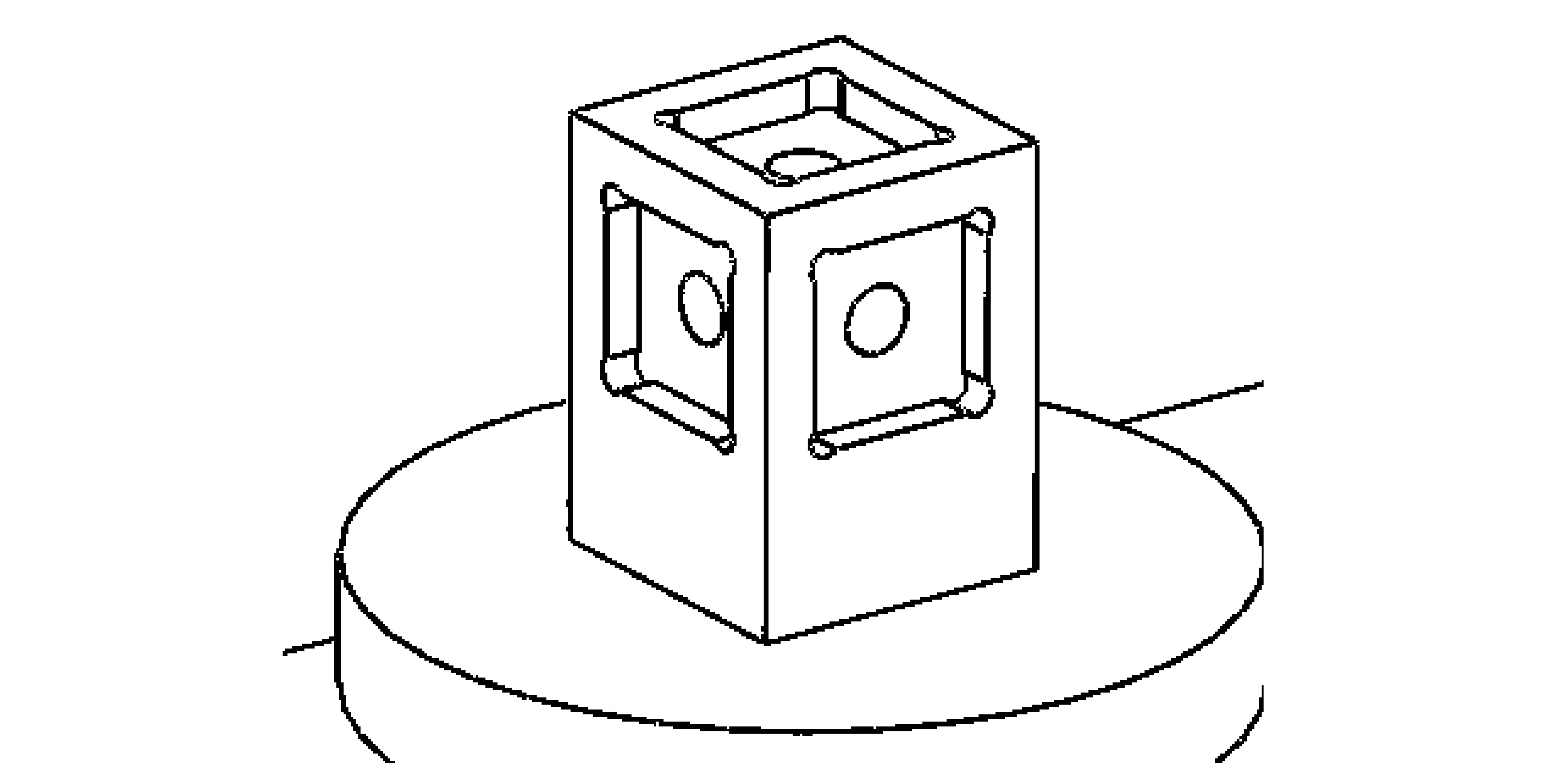
The material of the base is titanium alloy. It comes with a convex platform structure, as shown in Fig.3. At the top of the base and two adjacent sides there are circular air holes and installation groove. The diameter of the hole is less than the length of membrane of the chip. The length of the groove is longer than the length of the chip. The three chips orthogonal pasted in the slot to measure the triaxial acceleration.

Fig.3 Structure of the base
1.3 Connection between the internal and external circuit
The deformation quantity of the chip is converted into voltage to outlet. So the flexibility lug plate is an important component to form the electrical path between the chip and the outlet. The lug is polyimide materials. The rolled copper, by etching process, will become the conductive stripes on the surface of the material paste. The surface of the stripes is processed by ENIG. Rolled copper have good ductility, so the lug have good advantages of elasticity and no circuit breaker. Polyimide has good tensile strength. This processing technology replaces the traditional way of welding, so the whole inner circuit system has good stability under the high impact.
1.4 Overall structure and advantages
This structure is a miniature of combined structure; the overall size is no more than 25 mm3. There are four important parts in this structure, including chips, base, lug and outlet.
The development of the process includes MEMS technology, metallic packaging, PCB, micro assembly process, the traditional welding process and potting and so on. This structure has smaller measurement error than the multi-sensor modes, and simpler decoupling algorithm than single-chip integration model of triaxial accelerometer.
2 Simulation analyses
The parts of base and lug are made of good intensity material, so the finite element analysis is aimed at the chip, including static mechanical analysis and model analysis. The purpose of the FEA is to test the chip’s impact strength, inherent frequency and locate the piezoresistor.
2.1 Static mechanical analysis
ANSYS software is used to analysis mechanical characteristics of the chip. Material property are initialized as follows: the density of silicon is 2.33×10³kg/m3,Young modulus of silicon is 130×103MPa, Poisson ration of silicon is 0.278[3], model element type is set to solid 95 200 nodes, 3D unit. The framework of chip’s back is set fix and thezaxis direction of the chip is loaded 30 000g, 60 000g, 90 000g, 120 000g, 150 000g, and 200 000ggravity acceleration. Tab.1 shows the result of the finite element analysis.

Tab.1 Results of simulation
Tab.1 shows the stress values are less than the limit of the yield strength of the silicon and the strain values are less than 1 000 με. These values are theoretical values. The acceleration value is in direct proportion to the stress value or the strain value, so the chip can work well under high impact.
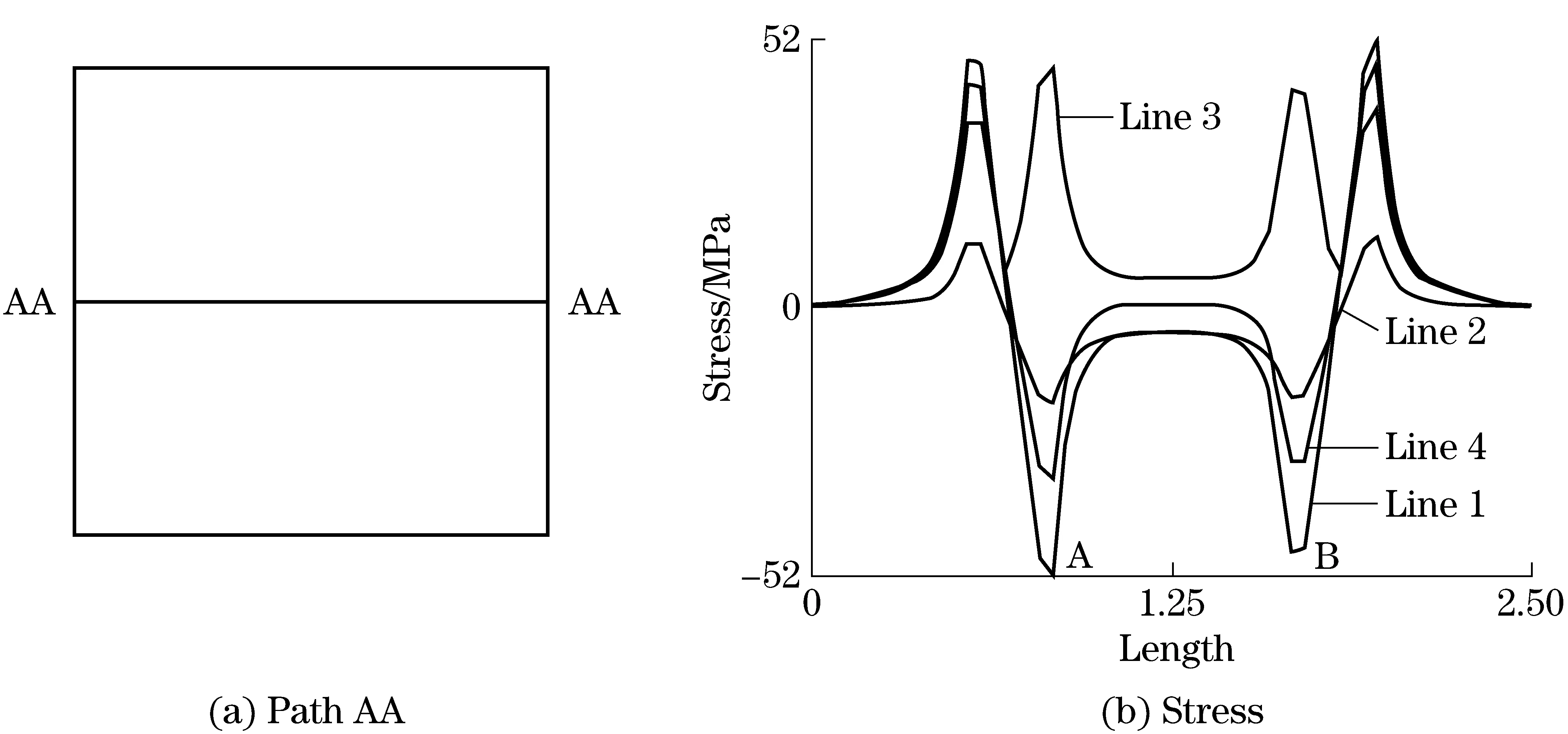
Fig.4 shows the curves of stress change along the specified path. Fig.4a shows the path AA on the chip surface, Fig.4b shows the result of the stress change.

Line 1——SX; line 2——SY; line 3——SEQV; line 4——SX-SYFig.4 Curves of stress change
Fig.4 shows the area of stress concentration, so the peak of the curve determines the location of the piezoresistors and form the Wheatstone bridge. Line 1 curve is the stress change ofσx, line 2 is the stress change ofσy, line 3 is vonmise stress, line 4 is the difference between A and B. The difference is calculated to get resistance variation in the previous formula.
2.2 Model analysis
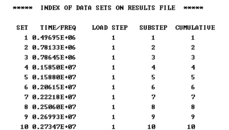
In practical, the operating frequency range is determined by chip’s inherent frequency. The higher natural frequency is, the wider working frequency is. Generally speaking, inherent frequency is 10 times of the working frequency[4]. Model analysis is used to study the inherent frequency of the chip. Fig.5 shows the simulation results of the model analysis. The value of first-order natural frequency is 496.95 kHz. This value is far away from low frequencies ranging, so the chip has good stability. The main direction of vibration iszaxis reciprocating motion, and this kind of situation is in according with design idea. The second-order and third-order vibration frequencies are about 300 kHz higher than first-order mode, so these vibrations mode show the effective inhibition of transverse which makes the chip work well[5].
2.3 FEA of the base
The value of titanium alloy tensile strength is 895 MPa and the shear strength is 670 MPa, the base ledge is the role of the beam under high impact, so the base needs to be analyzed in lateral resistance to impact.The result of the analysis is reasonable and shown in Tab.2. The strength of the base structure meets high-gimpact.

Fig.5 Model analyses
Tab.2 Analysis of base

LoaddirectionValueofimpactσx/MPaσy/MPaσz/MPax100000g364.045217.303323.791y201.932330.171307.412
3 Experiment and discussion
The MEMS-combined triaxial high-gaccelerometeriscalibratedbyusinganaircannon.ThisequipmentcangenerategreaterimpactenergythantheHopkinsonbar.Laserinterferometerisusedtomeasurethevelocityinthewholeexperimentprocess.Thelaserwaveformisdifferentialtogaintheaccelerationvalue.Aircannoncanoutputtensofthousandsofgshockload.Whentheloadeffecttothechip,thechipisindeformation,theaccelerometeroutputthethree-wayvoltage.Thevoltageiscorrespondingtotheaccelerationvalue.Theexperimentrepeatsmanytimes.Theexperimentresultsofmaximumofhigh-gimpactareshowninFig.6.

Fig.6 Results of experiment
Fig.6ashowsthewavebeforefilter,Fig.6bshowsthedataafterfilter,sothelineissmooth.Laserinterferenceprincipleisusedtomeasurethevelocityinthisexperiment.Line1istheoutputvoltageofzaxisdata;line3istheoutputvoltageofxaxisandline2istheoutputvoltageofyaxis,theaccelerationcurveisobtainedbyintegratingthelasersignalcurves,thezaxismaximumaccelerationismeetingtherequirementsofhighgvalues,andtheoutputvoltageisabout1.6V,sotheacceleratorhasagoodsensitivity.Theyaxismaximumvoltageis0.263Vandthexaxismaximumvoltageis-0.361V,sothelateralcoupledismorethan20%.Thisdataisslightlybiggerintestfield.Anefficientmethodwillbeadoptedtoreducetheparameter.Thesecondhalfofxaxiscurveisabnormal,thereasonisthattheinsulationlayeroftheouterleadisbroken,whichcausesshort-circuit[6].
4 Conclusion
TheMEMS-combinedtriaxialhigh-gaccelerometerisdesignbasedonthepiezoresistiveprincipleandthedevelopmentprocessesincludingMEMStechnology,PCBmanufacturingprocess,mechanicalprocesses,microassemblyandsoon.Itinheritsvariousadvantagesofpiezorsistivesensor,suchasgoodlinearity,highsensitivity,andsimplestructureandsoon.Thehighnaturalfrequencyandthehighimpactstrengthofthecombinedstructureareachievedthroughfiniteelementanalysisandexperimentverification,howevertheprocesstechnologystillneedstobeimprovedtoavoidtheoccurrenceofshortcircuitandthecrosscoupling[7]needstobereducedbyaddingthedecouplingalgorithm.
[1] Li R, Chen K, Kang X G, et al. Hard target smart fuze detonating control summary[J]. Journal of Detection and Control,2010,32(6):1-4. (in Chinese)
[2] Li K J. Modern sensor technology[M]. Beijing: Publish House of Electronics Industry, 2005. (in Chinese)
[3] Cheng Q X.Experimental research on ultra-precision grinding technology for silicon wafer tinning[D]. Dalian : Dalian University of Technology, 2013. (in Chinese)
[4] Shi Y B, Zhu Z Q, Liu X P, et al. Design and impact analysis of a high-gaccelerometer[J]. Explosion and Shock Waves, 2010,30(3): 329-332. (in Chinese)
[5] Li P, Shi Y B, Zhu Z Q, et al. An optimization method for natural frequency of MEMS high-gaccelerometer[J]. Chinese Journal of Sensor and Actuators,2013,23(3): 388-392. (in Chinese)
[6] Fan J B, Zu J, Lin Z S, et al. Shock calibration for a high-gaccelerometer using a laser interferometer[J]. Journal of Vibation and Shock,2012,31: 149-153. (in Chinese)
[7] Wu Z C, Ge Y, Yu C D. E-type 3-D accelerometer’s design based on thick film technology[J]. Sensor Technology,2011,9:3-7. (in Chinese)
(Edited by Wang Yuxia)
10.15918/j.jbit1004-0579.201524.0401
TP 212 Document code: A Article ID: 1004- 0579(2015)04- 0427- 05
Received 2014- 05- 23
Supported by the National Natural Science Foundation of China (61273346);the National Defense Major Fundamental Research Program of China (20110003);the National Defense Key Fundamental Research Program of China (20132010);Specialized Research Fund for the Doctoral Program of Higher Education (20121101120009); Excellent Young Scholars Research Fund of Beijing Institute of Technology (2012YG0203); the Program for the Fundamental Research of Beijing Institute of Technology (2015CX02034)
E-mail: zhzhang@bit.edu.cn
 Journal of Beijing Institute of Technology2015年4期
- Journal of Beijing Institute of Technology的其它文章
- Influence of shear sensitivities of steel projectiles on their ballistic performances
- Dynamic modeling and simulation for the rigid flexible coupling system with a non-tip mass
- Multi-constrained model predictive control for autonomous ground vehicle trajectory tracking
- Estimating the clutch transmitting torque during HEV mode-switch based on the Kalman filter
- Optimal tracking control for automatic transmission shift process
- High-precision method of detecting motion straightness based on plane mirror interference
