
β-Ga2O3 junction barrier Schottky diode with NiO p-well floating field rings
2023-12-15 11:48:26QimingHe何启鸣WeibingHao郝伟兵QiuyanLi李秋艳ZhaoHan韩照SongHe贺松QiLiu刘琦XuanzeZhou周选择GuangweiXu徐光伟andShibingLong龙世兵
Chinese Physics B 2023年12期
关键词:刘琦
Qiming He(何启鸣), Weibing Hao(郝伟兵), Qiuyan Li(李秋艳), Zhao Han(韩照), Song He(贺松),Qi Liu(刘琦), Xuanze Zhou(周选择), Guangwei Xu(徐光伟), and Shibing Long(龙世兵),†
1School of Electronic and Information Engineering,Beihang University,Beijing 100191,China
2School of Microelectronics,University of Science and Technology,Hefei 230026,China
Keywords: gallium oxide,Schottky barrier diode,nickel oxide,floating field rings
1.Introduction
The evolution of power electronic devices has largely relied on advanced semiconductor materials to meet the continuous needs for lower power loss, higher power density, and higher withstand voltage devices.Over the past decade,betaphase gallium oxide (β-Ga2O3) has gained increasing attention due to its unique material properties and cost-effective melt growth methods.[1]The theoretical critical field strength ofβ-Ga2O3is several times higher than that of other power device materials such as Si, SiC, and GaN, reaching up to 8 MV/cm, mainly attributed to its ultra-wide bandgap of 4.5 eV-4.9 eV.[2-5]In particular,the Baliga figure of merit exceeding 3000 implies the potential ofβ-Ga2O3for power device application.Additionally,even more exciting news is that the donor concentration ofβ-Ga2O3epitaxial films can potentially be controlled at even lower levels thanks to new growth methods[6]and carrier compensating technology.[7]This could further enhance the voltage rating ofβ-Ga2O3devices.
Power Schottky barrier diode(SBD),one of the most anticipated device types forβ-Ga2O3,always faces the challenge of electric field management.Localized high electric fields in SBD can lead to additional power loss and even catastrophic breakdown, leading to its performance much lower than the projected theoretical limit of the semiconductor.This issue is particularly severe forβ-Ga2O3SBD due to its higher critical breakdown field.In detail, the crowding electric field at the anode edge of the SBD results in a lower average electric field when the device breakdown.Not only that, even if the edge effect is ignored,the high electric field in the central anode region ofβ-Ga2O3SBD can cause a great barrier lowering,and the Schottky barrier, usually with lower energy, will lose its ability to block carriers, eventually leading to the soft breakdown of the device.
In response to the aforementioned challenges, numerous edge termination and reduced surface field (RESURF)structures have been developed forβ-Ga2O3SBD.The main edge termination structures include field plate(FP),[8-11]resistive termination,[7,12-16]guard ring,[17,18]high barrier anode edge,[19]mesa termination,[20-22]junction termination extension(JTE),[23-26]and floating field rings(FFRs).[27-29]As for the surface field control of the main Schottky junction, there are feasible solutions such as metal-oxide-semiconductor(MOS)type trench fin,[30-32]and heterojunction barrier Schottky diode.[28,33-35]Unfortunately, the performance ofβ-Ga2O3SBD still falls short of the predicted level.In order to fully leverage the advantages ofβ-Ga2O3,it is necessary to improve the material quality and develop electric field modulate structures.
In commercial power diodes, junction barrier Schottky(JBS) diodes combined with JTE and FFRs, which bring a low leakage current and high avalanche ruggedness, have been generally recognized.However,the difficulty in achieving conductive p-typeβ-Ga2O3has, to some extent, limited the structural diversity ofβ-Ga2O3SBDs.Currently, p-type wide bandgap semiconductors represented by NiO have been proven to form heterojunctions withβ-Ga2O3, serving as a viable alternative.[36-41]In this work, we developβ-Ga2O3junction barrier Schottky diodes with NiO p-well floating field rings (JBS-FFRs), providing a feasible electric field management solution.We experimentally demonstrated the electrical performance advantages of the device, and furthermore,identified the optimization direction of the designed structure through TCAD simulation methods.
Figures 1(a) and 1(b) illustrate the schematic crosssectional image and plan-view optical micrograph of the JBSFFRs.The anode of the device is mainly composed of the JBS of the central electrode and the FFRs at the edge of the electrode.Below the central electrode lies a circular NiO p-well array with a depth of 0.4µm,in which the gap of the p-wells(GT)in the array is designed to be 3µm,4µm,and 5µm for comparative studies.The gap between the p-well FFRs (GR)is 2µm,with the same depth as JBS.Additionally,each p-well is equipped with NiO p-type field plate with a length(LFP)of 2 µm.Figures 1(c)-1(d) illustrate the operating mechanism of each structure in the JBS-FFRs under reverse bias.First,the NiO/β-Ga2O3circular p-well array under the anode can pinch-off the current path under the metal/β-Ga2O3Schottky diode between them,thereby reducing the surface field of the Schottky junction,[42]as shown in Fig.1(c).In addition, the fabricated NiO p-well FFRs surrounding the anode can spread the edge depletion region,[43]resulting in a reduced electric field, as shown in Fig.1(d).More importantly, the horizontal NiO p-type FP interacts with the trench sidewall lateral PN junction reduces the electric field at the trench corners and FP edges of the p-wells,as shown in Fig.1(e).Thanks to the lateral hetero p-n junction and p-type FP structure, the trench FFRs design may have greater potential spreading and edge field modulation capabilities than the planar structure.
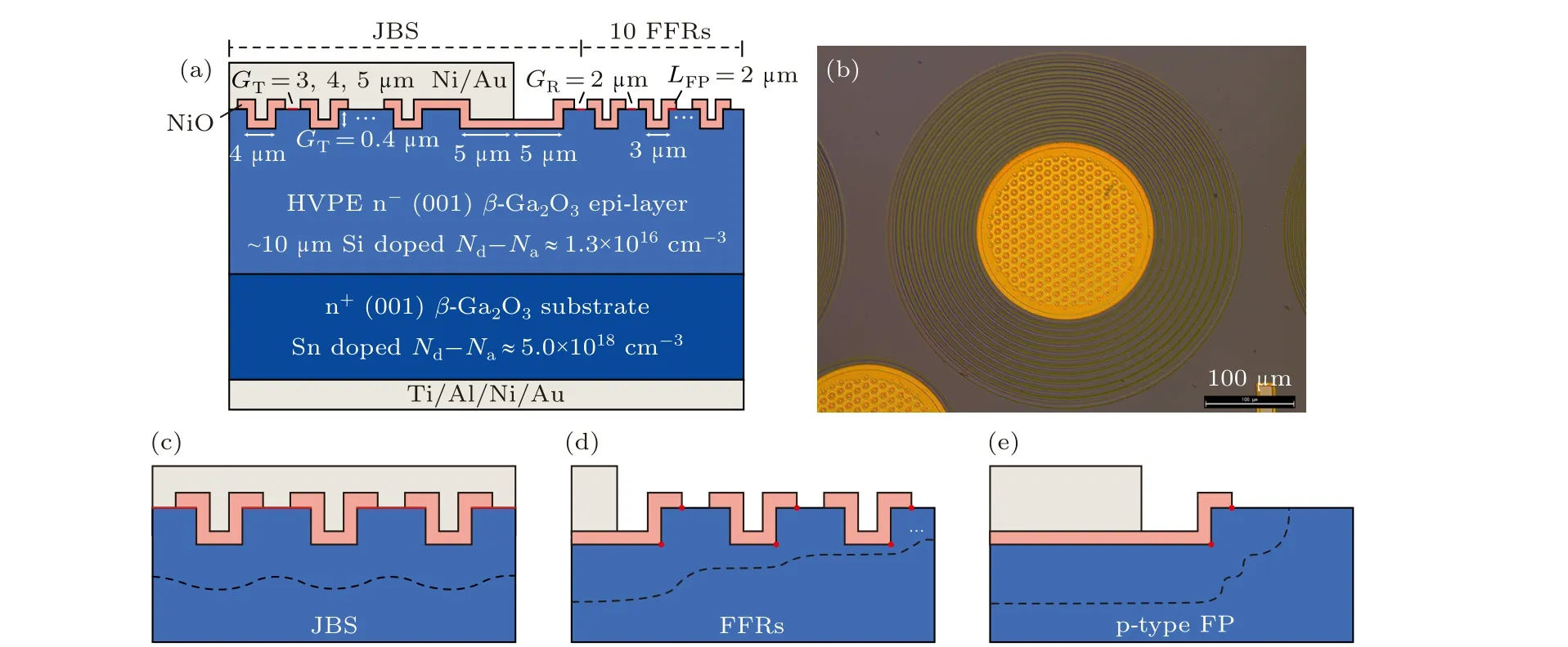
Fig.1.(a)The schematic cross-sectional image and(b)plan-view optical micrograph of the JBS-FFRs.The operating mechanism(reverse bias)of(c)p-well array,(d)floating field rings,and(e)NiO p-type field plate.The dashed lines and red point(or line)indicate the depletion region boundary and mainly electric field modulated position,respectively.
2.Device fabrication
The wafer used in this work,commercially available from Novel Crystal Technology, Inc., consists of a∼10 µm epitaxial layer grown on 640 µm high net doping concentration(Nd-Na,∼5×1018cm-3)β-Ga2O3substrate by halide vapor phase epitaxy.The epitaxial layer serves as a drift layer withNd-Naof∼1.3×1016cm-3.The device fabrication started with solvent, and piranha solution cleaning, followed by Pt metal alignment mask deposition.Next,the trench rings and circle trench array with 400 nm depth were formed by dry etching and immediately followed by soaked in piranha solution for 15 min to remove the dry etch damage.Afterward,the wafer was soaked sequentially in a piranha solution for 15 min and then in a buffered oxide etch(BOE)solution for 30 min to repair etching damage.Then,Ti/Al/Ni/Au(20/160/40/80 nm)cathode metal was evaporated by electron beam, followed by a 470◦C,1-min annealing process to form an ohmic contact.
After completing the above process,p-wells were formed by depositing 270 nm thick p-type NiO on the anode side,which filled the circular trench array and trench rings.This depositing process used a high-purity NiO target and was performed in a mixture of Ar/O2(2:3)room temperature ambient to achieve a relatively high hole concentration of NiO.The RF power used during the experiment was 200 W,and the growth pressure was maintained at a fixed level of 3.7 mtorr.Based on the O 1s XPS spectrum,the NiO film exhibited p-type conductivity and demonstrated non-stoichiometric characteristics,with a Ni3+/Ni2+ratio of about 1.5.[39]To create the p-type FP structure, the edge of the NiO film was extended over 2 µm beyond the trench edge.Finally, Ni/Au (100/150 nm) anode metal with a 100 µm radius was evaporated by the electron beam.It is theoretical to form Schottky contact withβ-Ga2O3and form ohmic contact with NiO.
The inset graph of Fig.2(a)shows the optical micrograph of a transfer length method(TLM)structure fabricated on the same wafer as the devices.This TLM test structure consists of a NiO film strip and several 100×70µm Ni/Au square electrodes, the distance between the two electrodes ranges from 5 µm to 45 µm with a step of 5 µm.Figure 2(a) displays the scanning current-voltage (I-V) results of the TLM structure, ranging from-10 V to 10 V.It can be found that all curves exhibit approximately linear behavior, indicating the ohmic contact between Ni/NiO.Figure 2(b) shows the total resistance between electrodes as a function of electrode gaps.The output resistance has shown strong linear dependence on electrode spacing,and the TLM data was fitted to extract contact resistance(RC=1.0 kΩ·mm), specific contact resistance(ρC=16.8 mΩ·cm2),and sheet resistance(Rsh=705.2 kΩ/⬆)of NiO film.Although theI-Vresults of TLM exhibit Ohmic contact characteristics, the values ofRCandRsh, as an active region total resistance component,are still relatively high,which could potentially impact the on-state performance of the device.In addition,the Ni/NiO may still be a Schottky contact with low barrier height, which will be discussed later in this article.
In addition to devices shown in Fig.1(a), SBD without edge termination (regular SBD), NiO/β-Ga2O3heterojunction PN diode (PND), and JBS diode without FFRs (JBSD)were also fabricated as comparison devices.The low-voltage(≤200 V)I-Vcharacteristics of the devices under dark conditions were measured using the Keysight B1500A Semiconductor Device Analyzer, while the breakdown voltage (Vbr) was measured using the Keysight B1505A power device analyzer.To avoid premature breakdown caused by surface flashover,the devices were submerged in Fluorinert FC-770 during the measurement.
3.Forward characteristics
Figures 3(a) and 3(b) present the room temperature forward current density-voltage(J-V)characteristics of the fabricated devices in liner and semi-log scale,respectively.It can be observed that the turn-on voltage of SBD is significantly smaller than that of PND, while all JBS-FFRs exhibit an apparent two-stage turn-on characteristic.The voltage at the first turn-on is the same as SBD, about 1.1 V.And the voltage at the second turn-on is consistent with that of PND,about 2 V.Moreover, figure 3(b) demonstrates that the ideality factor of the PND is approximately 2,indicating that the current is contributed by both majority and minority carriers,while the SBD has an ideality factor of nearly 1, indicating that the current is mainly contributed by majority carriers.In contrast, the JBS-FFRs diode shows consistency with the SBD, implying that the current before its second turn-on primarily originates from its SBD component.Furthermore, we find that the current prior to the second turn-on is correlated with the ratio of the NiO p-well area(GT=3µm,∼50%;GT=4µm,∼45%;GT=5 µm,∼40%) in the central anode.A greater proportion of the p-well area leads to a smaller current, which features similar to the merged PiN Schottky diode.The Schottky barrier diode(SBD)has a barrier height of 1.27 eV,while the JBS-FFRs withGTof 3µm,4µm,and 5µm have higher barrier heights of 1.41 eV,1.40 eV,and 1.34 eV,respectively.The increase in barrier height observed in JBS-FFRs compared to SBDs can be attributed to the lateral PN junctions and sidewall surface states induced by the etching process of the pwells,which can deplete the carriers ofβ-Ga2O3between the p-wells.
The relationship between the specific resistance (Ron,sp)and applied voltage was further compared, as shown in Fig.3(c).The PND has lowerRon,spafter turn-on than the SBD, which may be caused by the carrier recombined at NiO/βGa2O3interface.[38]In addition,theRon,spof JBS-FFRs diodes decreases as the proportion of the p-well area beneath the electrode increases, and eventually becomes consistent with PND.The results above indicate that JBS-FFRs diodes are capable of not only maintaining the low turn-on voltage as SBD,but also achieving an even lower on-state resistance.Unfortunately,neither the JBS-FFRs diodes nor the PND measured a current higher than that of the SBD, which is mainly limited by the thermal effect of small size devices.Largersized NiO/βGa2O3PNDs have been reported to show significant conductance modulation effects.[44,45]Another issue is that the Ni/NiO ohmic contact resistance shown in Fig.2 is higher than theRon,spof PND and JBS-FFRs diodes.The mechanism under this measurement result is not understood at present,one possible reason is that the Ni/NiO contact fabricated in this work is not an ohmic contact but rather a Schottky contact with a relatively low barrier.This non-ideal contact will also limit the conductivity modulation performance of the devices.
To verify the impact of the FFRs on theI-Vcharacteristics, figure 3(d) compares the forward characteristics of JBS diode with(solid line)and without(dash line)FFRs.It can be found that adding FFRs hardly affects the forward characteristics of the device.This is also one of the advantages of the FFRs as an electric field modulate structure.
4.Reverse characteristics
The reverse characteristics of the devices are shown in Fig.4.By examining theJ-Vcharacteristic under a reverse bias voltage of 0 V-200 V displayed in Fig.4(a), we can observe that the leakage current of the JBS-FFRs diodes falls between that of PND and SBD.In addition,it also reveals that the smallerGRunder central anode, the smaller the device’s leakage current.This trend is anticipated, smaller gaps facilitate the pinch-off of the current path between p-wells,which in turn reduces the electric field of the Schottky junction.The principle behind this phenomenon is akin to the previously reported trench-fin structure.[31,46]However,limited by the process in this work,the gaps can hard be controlled below 2µm.Even if the used circular p-well array is expected to have a relaxed size requirement due to the 3-D nature of its RESURF effect.[47]To fully leverage the advantages of this structure,further narrowing of the gaps and deepening of the p-wells is required, while also identifying the optimal balance between them.
In Fig.4(b), the measured breakdown voltage of the devices is plotted.The JBS-FFRs diodes exhibited a higher breakdown voltage, reaching 1356 V, compared to SBD and PND.This was primarily attributed to the FFRs’ function to transfer potential and spread the depletion region at the edge of central anode.The optical micrographs of the JBS-FFRs diode experiencing catastrophic breakdown are shown in the inset image of Fig.4(b).It can be observed that the damaged region extends to the outermost edge of the FFRs, providing evidence that the FFRs are effectively functional.However,there is still a gap in the leakage current suppression capability between JBS-FFRs and PND,which is likely due to defects induced by the device fabrication process.
To determine the effectiveness of FFRs,we took into account the hole concentration and gap design between them,and both experiments and TCAD simulations were carried out.The hole concentration in NiO is related to its oxygen vacancy concentration.[39]Therefore, to reduce the carrier concentration of NiO,a 300◦C,5 min nitrogen annealing process was performed on the device.After annealing,theJ-Vtest results of the TLM structure showed a significant decrease in current as shown in Fig.4(c).Additionally, the breakdown points of all JBS-FFRs were found only at the edge of the central anode as shown in the inset image in Fig.4(c), indicating that the FFRs are nonfunctional.This result suggests that high hole concentration of the p-wells is conducive to potential transmission.
Figure 4(d)shows the results of TCAD simulations of the electric field distribution at the FFRs region when the device is under 1000 V reverse bias.The top image illustrates the electric field distribution when the net hole concentration(Na-Nd)of the p-well rings is 1×1019cm-3, theLFPand theGRare both 2µm.While the structural parameter mentioned can reduce the electric field at the edge of the central anode, it is only able to transfer the potential to a maximum of the third ring.By maintaining the hole concentration of the p-well rings and shortening both theLFPandGRto 1µm(as shown in the middle image), the last ring is still able to obtain potential,while also achieving a more uniform distribution of the electric field.Not only that,the electric field crowding at the main junction edge can be further reduced.Moreover, If the hole concentration of the p-well rings is reduced to 1×1016cm-3(bottom image),the highest electric field position shifts to the edge of the metal electrode,and the FFRs lose their function.This experiment encountered process limitations that made it difficult to further reduce the size of the FFRs while maintaining process accuracy.Nevertheless,the simulation results demonstrate that significant improvements in the performance of JBS-FFR diodes can be achieved through deeply optimizing doping concentration and size parameters.
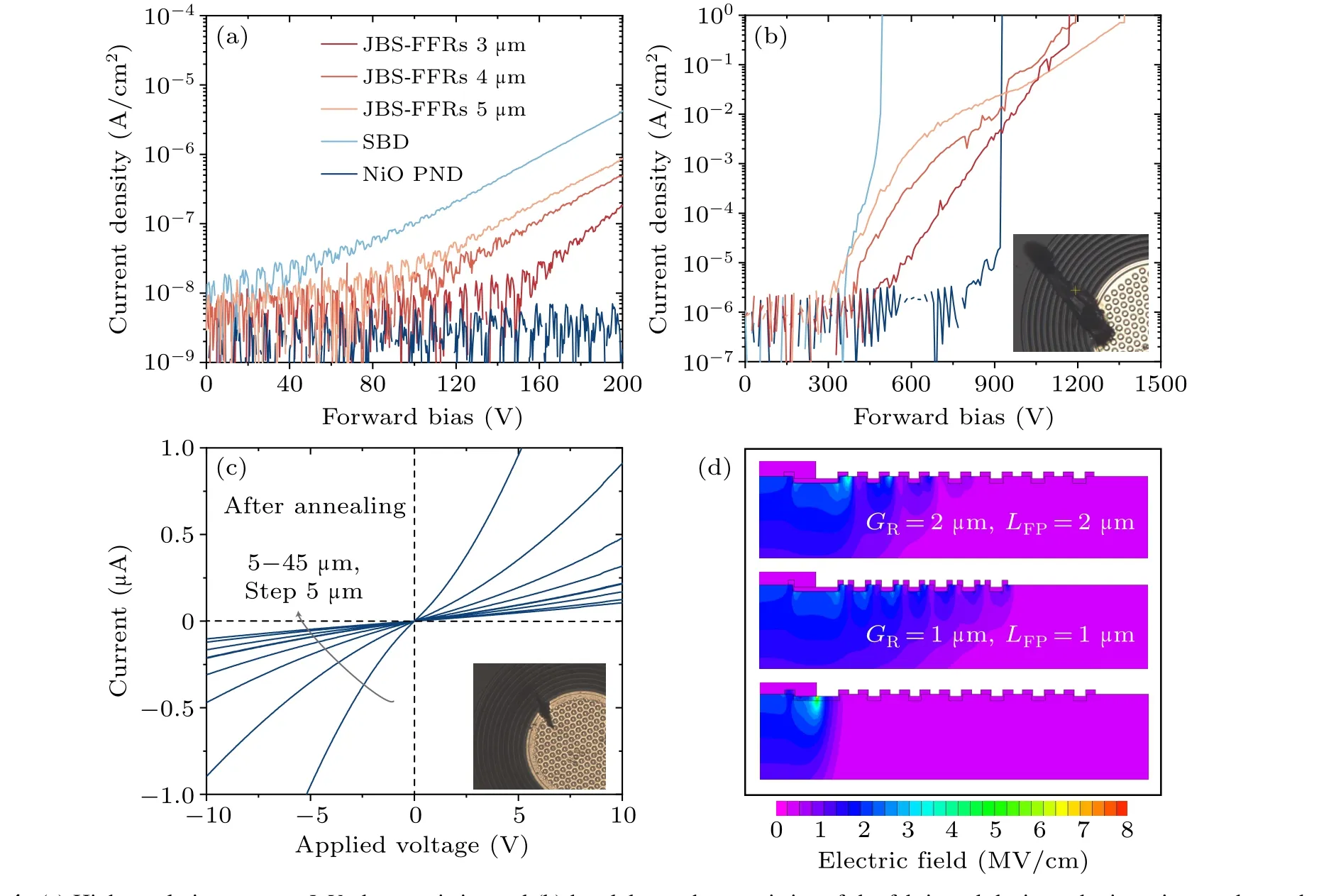
Fig.4.(a) High resolution reverse J-V characteristics and (b) breakdown characteristics of the fabricated devices, the inset image shows the optical micrographs of the JBS-FFRs diode after catastrophic breakdown.(c) The I-V results of the TLM structure were obtained after a nitrogen annealing process at 300◦C for 5 min.The inset image displays optical micrographs of the annealed JBS-FFRs diode after experiencing catastrophic breakdown.(d)The TCAD simulation results for the electric field in a JBS-FFRs diode with varying structural parameters of the pwell rings under 1000 V reverse bias.Na-Nd=1×1019 cm-3,GR=2µm,and LFP=2µm(top image);Na-Nd=1×1019 cm-3,GR=1µm,and LFP=1µm(middle image);Na-Nd=1×1016 cm-3,GR=1µm,and LFP=1µm(bottom image).
5.NiO field plate simulation
The NiO p-type FP designed in this work can be a good choice for modulating the electric field at every p-wells’edge.Figure 5(a) shows the TCAD simulation results of the electric field profiles at the central anode edge under a reverse bias voltage of 1000 V,demonstrating the function of the field plate.It can be observed that after adding a 2 µm FP, the highest electric field point has shifted from the trench bottom edge to the edge of the FP,and the value decreased.This phenomenon is mainly attributed to the interaction of the FP and the lateral PN junction on the sidewall of the trench, which causes the depletion region to expand.Due to the finite depletion region width of the NiO/β-Ga2O3junction under a specific bias voltage, it means that the performance of this edge structure is related to both the trench depth(DT)and the length of the field plate (LFP) when the material parameters and applied voltage are determined.
To determine the optimal size parameters of the structure,we simulated the relationship amongLFP,DT,and the highest electric field.TheNa-Ndof NiO was set to 1×1019cm-3with a thickness of 250 nm in this simulation.TheLFPandDTare range from 0µm-2µm with a step of 0.25µm.Figure 5(b)illustrates the highest electric field map when a reverse bias of 1000 V is applied to the anode.The dark blue area is the best structural parameter forLFPandDT.Unfortunately, the devices fabricated in this work were not at the optimal positions due to process limitations,we are still finding a way to address the process issue.
It should be noted that this simulation did not consider the additional impacts of interface states at the trench sidewall,which may be caused by the etching process,as well as variations in the concentration of holes in NiO, on the electric field.A more comprehensive analysis that takes these factors into account may provide a more accurate representation of the structure’s behavior.Moreover, when applying the FP structure to FFRs,a better distribution of electric field is necessary to further clarify the design formulas for the structure and material parameters of each level of the FFRs.Therefore,there is still a lot of room for optimization of JBS-FFRs diode.
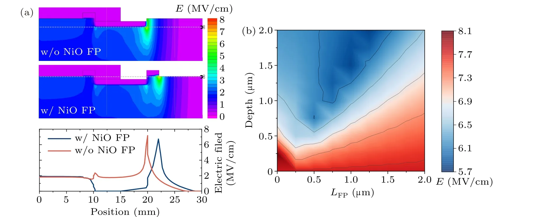
Fig.5.(a)Simulated electric field profiles of the device with and without p-type NiO FP.(b)The highest electric field versus LFP and DT under reverse bias of 1000 V.
6.Conclusion and perspectives
In conclusion, in order to address the high electric field issue ofβ-Ga2O3SBDs,we have developed aβ-Ga2O3JBSFFRs diode, and its electrical characteristics have been studied.Experimental results indicate that with the joint support of the p-well array, p-well FFRs, and NiO FP, the device’s breakdown voltage and leakage suppression capability were improved.In addition,we further combined TCAD simulation tools to clarify the optimization direction of the JBS-FFRs.This work demonstrated that the designed device has a positive effect on the electric field uniformity inβ-Ga2O3SBDs,which is beneficial for further advancing the performance of gallium oxide devices.
Acknowledgements
Project supported by the National Natural Science Foundation of China (Grant Nos.61925110, U20A20207,62004184,62004186,and 62234007),the Key-Area Research and Development Program of Guangdong Province (Grant No.2020B010174002), the funding support from University of Science and Technology of China (USTC) (Grant Nos.YD2100002009 and YD2100002010), the Fundamental Research Plan (Grant No.JCKY2020110B010), Collaborative Innovation Program of Hefei Science Center, Chinese Academy of Sciences(Grant No.2022HSC-CIP024),and the Opening Project of and the Key Laboratory of Nanodevices and Applications in Suzhou Institute of Nano-Tech and Nano-Bionics of CAS.This work was partially carried out at the Center for Micro and Nanoscale Research and Fabrication of USTC.The author would like to express gratitude to those who assisted and encouraged during research work, with special appreciation to Prof.Xiaojun Wu and Prof.Liu Ming.
猜你喜欢
Plasma Science and Technology(2023年3期)2023-03-15 00:54:16
作文周刊·小学二年级版(2022年24期)2022-06-18 14:30:28
客联(2022年3期)2022-05-31 03:58:03
江苏科技报·E教中国(2022年5期)2022-05-11 22:54:28
儿童故事画报(2022年3期)2022-04-27 22:55:19
Chinese Physics B(2021年9期)2021-09-28 02:18:04
Chinese Physics B(2021年5期)2021-05-24 02:23:04
Chinese Physics B(2021年3期)2021-03-19 03:21:58
Acta Mathematica Scientia(English Series)(2018年3期)2018-07-23 08:41:10
水动力学研究与进展 B辑(2018年1期)2018-04-13 12:23:48

- Chinese Physics B的其它文章
- Diamond growth in a high temperature and high pressure Fe-Ni-C-Si system: Effect of synthesis pressure
- Si-Ge based vertical tunnel field-effect transistor of junction-less structure with improved sensitivity using dielectric modulation for biosensing applications
- Speeding-up direct implicit particle-in-cell simulations in bounded plasma by obtaining future electric field through explicitly propulsion of particles
- Temperature-induced logical resonance in the Hodgkin-Huxley neuron
- Energy-distributable waterborne acoustic launcher for directional sensing
- Structural stability and ion migration of Li2MnO3 cathode material under high pressures