A laser-produced plasma source based on thin-film Gd targets for next-generation extreme ultraviolet lithography
Xiao CHEN (陈笑), Yao LI (黎遥), Jianbo HOU (侯鉴波), Zhe ZHANG (张哲),Xianyang LU (陆显扬), Yu YAN (严羽), Liang HE (何亮) and Yongbing XU (徐永兵)
Jiangsu Provincial Key Laboratory of Photonic and Electronic Materials Sciences and Technology,School of Electronic Science and Engineering, Nanjing University, Nanjing 210093, People’s Republic of China
Abstract
Keywords: extreme ultraviolet light source, laser-produced plasma, gadolinium
1.Introduction
Extreme ultraviolet (EUV) lithography has been a key technology for the semiconductor industry, which enables the volume manufacture of large-scale integrated circuits with feature sizes below 14 nm.According to the Rayleigh formula(CD=k×λ/NA),it is possible to employ short-wavelength light sources to reduce the critical distance (CD) of the chip,in addition to raising the numerical aperture (NA) of the optical system.The development of high-efficiency and lowdebris EUV light sources is one of the critical requirements for the EUV lithography system.At present, the laserproduced plasma (LPP) of tin (Sn) targets has been successfully applied as the EUV light source in current lithography systems [1].When the Sn target is heated to 30-50 eV by a high-power laser, the plasma can produce strong emissions with a peak wavelength at 13.5 nm [2], which matches with the reflective band of available Mo/Si multilayer mirrors[3].The emission features make Sn plasma the advisable solution for high-power EUV light sources.To further advance the semiconductor process to smaller nodes, the next-generation light source beyond the EUV(<10 nm)has been added to the research agenda.With the development of La/B4C multilayer mirrors, a high reflectivity of 20%-40%has been obtained at 6.5-6.7 nm, and achievement of a theoretically higher reflectivity of 80% is possible.Therefore, the relative wavelength band coupled with these mirrors is deemed the suitable wavelength for the next stage of the beyond EUV(BEUV) light source [4, 5].Gadolinium (Gd) plasma heated to over 100 eV can generate thousands of emission lines centered at 6.7 nm [6], which makes it one of the most appropriate candidates for BEUV lithography.
At present,there are some works that have been reported to obtain a BEUV light source at 6.7 nm based on the LPP of Gd targets [7-10].Similar to the pioneering efforts of Sn plasmas,the goals of these efforts are either to improve the conversion efficiency (CE) of the Gd plasma or to reduce the debris produced during the excitation process.To pursue the two goals for practical applications,two main approaches have been proposed:optimization of the laser parameters [10-14], and choosing the appropriate form of the targets[10,15,16].With respect to the second approach,a mass-limited target is preferred as it can not only produce sufficient EUV emission but also reduce the neutral atoms and low-ionized ions that come from the deep layer of the target[17].There are several forms of mass-limited targets, such as sphere targets made by depositing materials on balls[18-21]or bubbles[22],thin-film targets coated on planar Si wafers or glass[23,24]and uniform liquid droplets[25,26].Comparably,the thin-film target approach is simpler,and it can be easily applied to the study of the properties of mass-limited targets made of new materials in the laboratory.By using masslimited thin-film targets, it is found that Sn targets that are several tens of nanometers thick, which are also named minimum-mass thin-film targets,are able to generate EUV radiation as efficiently as the planar bulk targets[18,27].However,until now,there have been few reports about the LPP of mass-limited thin-film Gd targets for the BEUV light source.
In this work, we have studied the LPP spectra of BEUV sources based on mass-limited thin-film Gd targets, which were prepared using the magnetron sputtering method.LPPs of the thin-film targets were excited by a high-energy neodymium-doped yttrium aluminum garnet (Nd:YAG) laser at 1064 nm.The influences of the laser intensity on the BEUV emission from thin-film targets were first investigated.When the laser intensity was changed from 6 × 10¹⁰to 3.37 ×10¹¹W cm−2, it was found that the CE of the LPP peaks at about 2 × 10¹¹W cm−2for the thin-film target.Then, the emission spectra of the LPPs were compared with Gd targets with different thicknesses.A minimum-mass target with a thickness of 400 nm was deduced by evaluating the CEs of LPPs, which further proved that this thickness may be the ablation depth for this kind of mass-limited target.These findings in this work may give us guidance on how to develop high-efficiency and low-debris BEUV light sources in the future.
2.Experimental setup
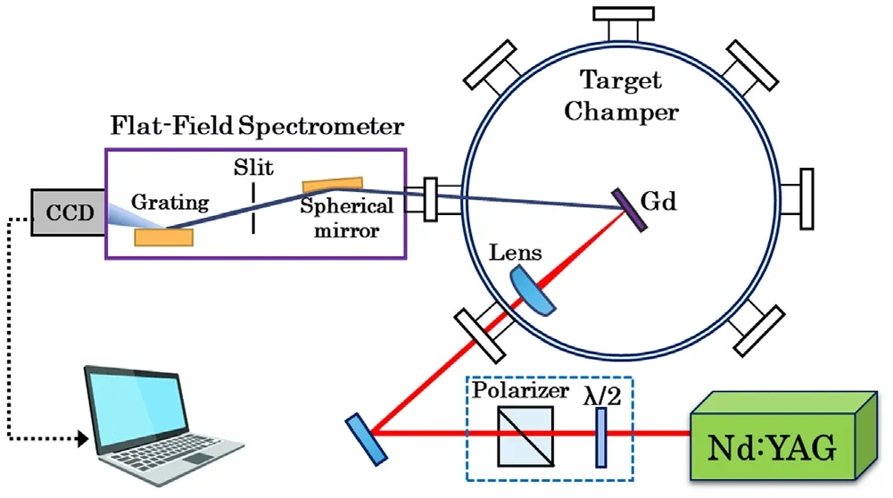
Figure 1.A schematic setup of the LPP based on thin-film Gd targets.
A schematic setup of the experiment is shown in figure 1.The target was irradiated by a high-energy Q-switched Nd:YAG laser operating in single-shot mode.The laser has a center wavelength of 1064 nm, a maximum pulse energy of 900 mJ and a pulse width of 7 ns.The laser beam was perpendicularly focused on the Gd targets by an anti-reflection (AR@1064 nm) plano-convex BK7 lens with a focal length of 15 cm.The focused laser diameter was determined by the ablative aperture of the target at a low incident energy of 1 mJ.In our experiment, the focused laser diameter at the target position was measured to be 165 μm by an optical microscope.To investigate the properties of the BEUV spectra under different laser intensities, the energy of the incident Nd:YAG laser was adjusted by rotating the halfwaveplate in front of the polarizer.
The thin-film targets used in this work were prepared using the magnetron sputtering method to deposit layers of Gd onto Si wafers.The steps to prepare the targets are as follows: first,3 cm×4 cm size Si wafers were used as the target substrate.All the substrates were cleaned with acetone, ethanol and deionized water before material deposition.Then, the Si substrates were deposited with thin layers of Gd via the magnetron sputtering equipment with an argon(Ar)pressure of 4.3×10⁻³mbar and an Ar flow rate of 20 sccm.A direct-current power of 60 W was applied to control the deposition speed of 0.25 nm s−1.The purity of the Gd source in the sputtering procedure was 99.99%.The thicknesses of the deposited Gd thin films were monitored by a quartz crystal with a precision of 0.1 nm.Finally,the Gd targets were fixed on an aluminum holder in the target chamber,and its position could be translated by X-Y linear stages to provide a fresh surface for each laser shot.
The vacuum of the target chamber was maintained by a molecular turbo pump (2200 l s−1, Leybold) connected to a forestage scroll pump (15 m3h−1, Edwards) to avoid the absorption of the generated BEUV radiation.The pressure of the target chamber was maintained in the range of 10−7mbar during the experiment.The BEUV spectra from the Gd plasmas were recorded by a flat-field spectrometer (FFS)positioned at 45 degrees with respect to the incident laser.The FFS consisted of a spherical collecting mirror, a variable spaced reflective grating (1200 l mm−1), a slit and a backilluminated x-ray charge coupled device (CCD) camera(Andor 940P).The CCD camera was thermoelectrically cooled down to −15°C to reduce the background noise.The typical spectral resolution of the FFS is ∼0.02 nm within the spectral range from 4 to 20 nm.
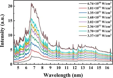
Figure 2.The BEUV spectra of the 300 nm thin-film Gd target.
3.Results and discussion
Typically,Gd plasma produces BEUV emission at 6.7 nm when its electron temperature is heated to over 100 eV, which can be controlled by the laser and target properties.Therefore,to obtain the best CE for the mass-limited targets,it is necessary to find the optimal experimental conditions,which are the laser intensity and the target’s thickness.First,we fixed the thickness of the target at 300 nm and measured the corresponding BEUV spectra from the LPP under different incident laser intensities.The spectra of the LPP, when the incident laser intensity is changed from 6.7 ×10¹⁰to 3.37 × 10¹¹W cm−2, are shown in figure 2.It can be seen that the peaks of the emission spectra are around 6.7 nm,which is mainly attributed to the 4d-4p and 4d-4f transitions in ions from Gd12+to Gd25+.It is also observed that the Gd spectra contain satellite emission lines at the wavelength of 7.17 nm when the incident laser intensity is increased.These emissions come from the n=4−n=5(Δn=1)transitions in ions from Gd19+to Gd27+[7,13],because the mean ionic charge state has been increased during the procedure.Moreover, when the laser intensity was increased over 2 × 10¹¹W cm−2, specific radiations in the 8-9 nm region were observed.This is because the Si substrate will absorb the residual incident laser and produce emissions due to the charged states from Si3+to Si8+.On the other side, a superposition of lines, including the Gd line at 5.9 nm and the Si lines at 4.55 nm, 4.8 nm and 5.2 nm [28],dominates the spectra in the range of 4.5-6 nm.
Based on the spectra,figure 3 illustrates the dependence of the CEs on the laser intensity within the 0.6% bandwidth at 6.7 nm [29].In this experiment, we used a spectrometer and calculated the relative CEs of the light source.First, we evaluated the intensity of the BEUV light of bulk targets under the same conditions as the experiment in[13],and considered the CE to be the same with a value of 0.4%.Then,the relative CEs in this work were obtained by comparing the BEUV radiant spectra from thin-film targets with those of the bulk targets.Although an accurate CE is preferred, it is found that the relative CEs are sufficient to obtain the laws of impacts by changing the laser’s and targets’ parameters.As seen in figure 3,the CEs of the thin-film targets increase with the laser intensity in the beginning and then saturate when the laser intensity reaches 2 × 10¹¹W cm−2.In these conditions, the optimal CE of the 300 nm thick Gd target is 0.54%.The results indicate that this threshold point should be the optimal laser intensity.This CE tendency is similar to that of Sn plasma,which also saturates at a dedicated incident laser intensity.The saturation of the CE is attributed to the self-absorption effect when the produced plasma is overheated.In this case,the plasma around the BEUV emission zone gets denser.Thus,the denser plasma will absorb the BEUV light and prevent the light from passing through the plasma.It should also be noted that the CE will gradually decrease when the laser intensity is further higher than the optimum conditions.
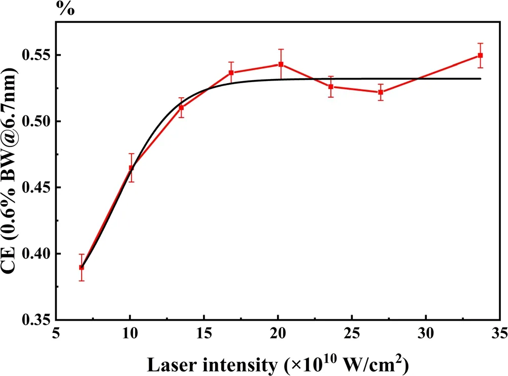
Figure 3.The CEs of the 300 nm thick Gd target under different laser intensities.

Figure 4.The BEUV spectra of the LPP from Gd targets with different thicknesses.
When the optimal laser intensity was preliminarily determined, the BEUV spectra of the mass-limited thin-film Gd targets with various thicknesses were recorded, as shown in figure 4.It is observed that there is a dip structure at 6.82 nm together with two peaks at 6.676 nm and 6.955 nm for targets with a thickness less than 200 nm.The dips gradually disappear as the thin-film Gd targets become thicker.This dip structure in the spectra is attributed to the re-absorption of BEUV light by the surrounding low-temperature plasma, which is formed by the atoms in the thin film below 200 nm.It can also be seen that the intensity of BEUV emission increases when the thickness of the target increases from 50 to 400 nm, and declines slightly from 400 to 500 nm.
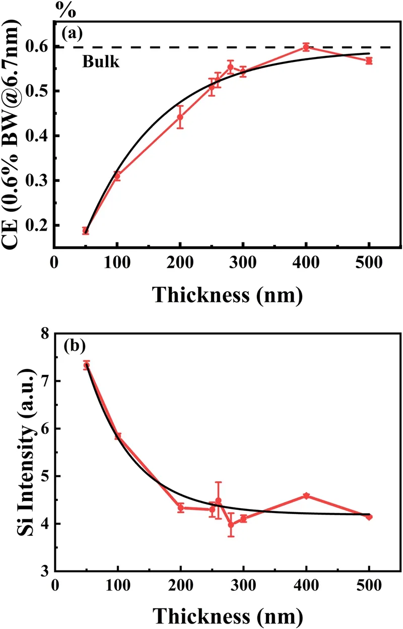
Figure 5.(a) The CEs of the Gd targets with different thicknesses,and (b) the intensity of the Si emission line at 11.786 nm.
Identically, the evolutions of the CEs of the thin-film targets with different thicknesses are illustrated in figure 5(a).It can be seen that the CE increases with the thickness in the beginning and reaches its peak of 0.6% at a thickness of 400 nm.There are some differences in the error bars for the data at different target thicknesses.This is because unavoidable errors in the installation position and angle are introduced when we change the target with different thicknesses.The spectrometer is comparably sensitive to the radiation position.Thus, when the target is moved for new data, there will be a slight fluctuation in the measured spectra.The CE of the Gd plasma from the bulk target is also shown in the figure as the dashed line (black).The CEs of the 400 nm target and the bulk target are comparable, which indicates that the 400 nm target is the minimum mass for the LPP emission under the current incident laser intensity of 2×10¹¹W cm−2.
This minimum-mass target’s thickness is, to a certain extent, connected to the ablation depth of the incident laser.The ablation depth can also be evaluated via the intensities of the Si emission lines in the spectra.When the thin-film target is thinner than the ablation depth, there will be observable emissions from the Si substrate.Thus,the emission lines from the 2p-3s transition of Si4+at 11.786 nm were extracted, as shown in figure 5(b) [28].It is observed that the intensity of this Si line dominates for Gd targets below 400 nm, which matches with the CE results in figure 5(a).
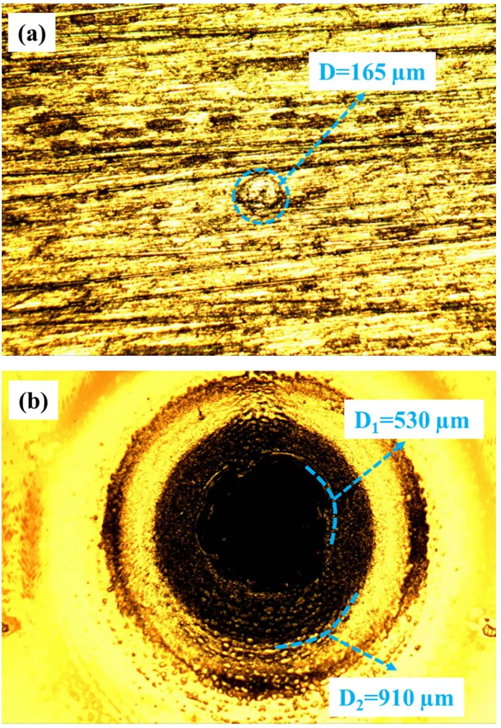
Figure 6.(a)A microscope photograph of the laser spot profile, and(b) a microscope photograph of the 400 nm Gd target irradiated under a laser intensity of 2 × 10¹¹ W cm−2.
The theoretical ablation depth for a thin-film target according to [18] is calculated as:
where Ia, λL, and τLare the intensity, wavelength and pulse width of the incident Nd:YAG laser, respectively, and ρ0is the initial density of the target.Under the present experimental conditions(Ia=2×10¹¹W cm−2,λL=1064 nm,τL=7 ns,ρ0=7.901 g cm−2),the theoretical ablation depth dais calculated to be 36 nm.It is found that the experimental ablation depth is greater than the calculation result,which we think is due to the small laser spot used in this experiment.The smaller laser spot, compared to [18] (165 μm versus 500 μm,assuming the same laser intensity),leads to greater expansion of plasma in the focal plane and deeper ablation on the target surface.As shown in figure 6(a),the incident laser has a focused diameter of 165 μm, measured by the ablative aperture of the bulk target at a low incident energy.Figure 6(b) displays the spatial profile of the ablated 400 nm target under an irradiated laser intensity of 2×10¹¹W cm−2.The ablated area of the thinfilm target has a larger diameter compared to the laser diameter,which is due to the expansion of the plasma in the focal plane.Thus,the plasma exhibits a two-dimensional expansion,leading to a much deeper ablation depth[14].In contrast,if a larger laser spot is assumed, the plasma will exhibit a one-dimensional expansion and a lower ablation depth can be expected.
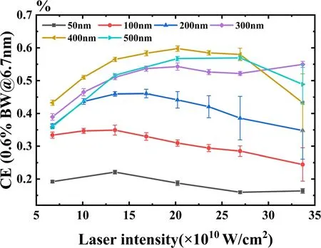
Figure 7.The CEs of thin-film Gd targets with different thicknesses under different laser intensities.
Finally, to consider the impact of laser spot size on the thickness of the minimum-mass target, we have analyzed the CEs for targets with different thicknesses while simultaneously varying the incident laser intensity,which is shown in figure 7.In general, the CEs of the targets increase with the incident laser intensity and then decrease gradually once the intensity goes beyond the optimal conditions.The exception of an increase near the highest intensities (>25 × 1010W cm−2) for the 300 nm target may be attributable to small measurement uncertainty,which is just a CE change of less than 0.03%in the experiment.From the figure, we can see that a higher laser intensity is needed to achieve the optimal CE for a thicker target.The maximum CE value of 0.6% was achieved for a 400 nm thin-film target under an incident laser intensity of 2×10¹¹W cm−2, which indicates that this should be the optimal experimental parameters for such thin-film Gd targets.
4.Conclusions
In conclusion,we have presented a BEUV light source based on LPP of mass-limited thin-film Gd targets,which were prepared by sputtering Gd on Si wafers.The influences of the laser intensity and the target thickness on the CEs of the thin-film targets were carefully investigated.It is found that a maximum CE value of 0.6%was achieved with a 400 nm thick target at an optimal incident laser intensity of 2×10¹¹W cm−2.It has been proven that the optimum mass-limited target is connected to the ablation depth of the LPP.It should also be expected that a thinner target will be possible in the future by optimizing the laser diameter.The advantage of using a thin-film Gd target is that it can generate sufficient BEUV emission that is comparable to the bulk target but potentially produces less debris.Therefore,the mass-limited Gd target is an important strategy to implement for the next-generation BEUV light source at 6.7 nm.
It is known that mass-limited tin-droplet targets are employed as LPP targets in current industrial EUV light sources.However, due to the substantially higher melting point of Gd (1312°C), the design and manufacture of a Gddroplet generator is more challenging.Therefore, thin-film targets can be proposed as an alternative solution, which can also be made into tapes with a soft substrate to meet the temporary requirement for repetitive targets for long-time operation.It should be noted that this work is a preliminary result.The CE should be a complex function of the laser parameters and target forms.It is necessary to optimize the parameters of the plasma source for further improvement of BEUV CEs,and a more accurate CE should be obtained using a calibrated calorimeter, which will be our next work.Moreover, it is also very interesting to investigate plasma evolution to better understand BEUV radiation in the future.
Acknowledgments
This work is supported by National Natural Science Foundation of China(Nos.61427812,61805118,12104216 and 12241403),and the Natural Science Foundation of Jiangsu Province of China (Nos.BK20192006, BK20180056 and BK20200307).
 Plasma Science and Technology2023年10期
- Plasma Science and Technology的其它文章
- 3D fluid model analysis on the generation of negative hydrogen ions for negative ion source of NBI
- Enhancing surface adhesion of polytetrafluoroethylene induced by two-step in-situ treatment with radiofrequency capacitively coupled Ar/Ar+CH4+NH3 plasma
- Etching characteristics and surface modification of InGaSnO thin films under Cl2/Ar plasma
- Pulsed gas-liquid discharge plasma catalytic degradation of bisphenol A over graphene/CdS: process parameters optimization and O3 activation mechanism analysis
- A homogeneous atmospheric pressure air plasma in a 10mm gap based on a threeelectrode configuration
- Effect of gas flow on the nanoparticles transport in dusty acetylene plasmas
