
Optimization of large-area YBa2Cu3O7−δ thin films by pulsed laser deposition for planar microwave devices
2023-09-05 08:48:32PeiYuXiong熊沛雨FuCongChen陈赋聪ZhongPeiFeng冯中沛JingTingYang杨景婷YuDongXia夏钰东YueFengYuan袁跃峰XuWang王旭JieYuan袁洁YunWu吴云JingShi石兢andKuiJin金魁
Chinese Physics B 2023年7期
关键词:王旭
Pei-Yu Xiong(熊沛雨), Fu-Cong Chen(陈赋聪), Zhong-Pei Feng(冯中沛), Jing-Ting Yang(杨景婷),Yu-Dong Xia(夏钰东),4, Yue-Feng Yuan(袁跃峰), Xu Wang(王旭), Jie Yuan(袁洁),Yun Wu(吴云),†, Jing Shi(石兢), and Kui Jin(金魁)
1School of Physical Science and Technology,Wuhan University,Wuhan 430072,China
2Beijing National Laboratory for Condensed Matter Physics,Institute of Physics,Chinese Academy of Sciences,Beijing 100490,China
3Songshan Lake Materials Laboratory,Dongguan 523808,China
4School of Physical Science and Technology,Southwest Jiaotong University,Chengdu 611756,China
Keywords: YBCO films,pulsed laser deposition(PLD),surface resistance,microwave devices
1.Introduction
In the past decades, there has been a significant focus on the technological applications of superconductors.With the significant advances in high critical temperature,high temperature superconductor (HTS) has come to various applications.[1–9]Among these, microwave applications of HTS films such as microwave transmission lines, filters,antennas and delay lines have great potentials, because the low microwave surface resistance(Rs)of HTS films provides the possibility of implementing microwave devices with ultranarrow band specification, which is extremely useful as the electromagnetic spectrum becomes more and more crowded nowadays.[10–12]Although theRsvalue of HTS thin films,especially YBCO thin films, is roughly two or three orders of magnitude lower than that of the normal conductors in the microwave frequency region, the key factors affectingRsare still unclear, and theRslimitation of the HTS thin film is not achieved.Many efforts on reducing theRsvalue of HTS films have been made.Artificial pinning center was introduced into the films to increase the critical current density and reduce theRsvalue,[13,14]Rsof Ca-doped YBCO thin films at 8.5 GHz showed a clear reduction compared to that of YBCO thin films,[15]and the microstructure corresponding toRscharacteristics was investigated.[16]Furthermore, models forRsin type-II superconductor were also constructed.[17]However,systematic investigations of the microwave characteristics are still needed to improve the applicability of superconducting microwave components for future technologies.
On the other hand, the quality of HTS films plays an essential role in microwave application, as the microwave devices based on HTS films are fabricated by semiconductor processing, requiring large size, good thickness uniformity, low defect rate and so on.In order to apply the advanced material to improve the microwave devices, lots of methods have acquired wide-spread acceptance as processes for growing various types of superconducting films, such as ion beam sputtering,magnetron sputtering,sol–gel,metal–organic chemical vapor deposition (MOCVD), pulsed laser deposition (PLD)and so on.[18–22]Among the above-mentioned methods, PLD provides a simple route for large-area film deposition.It not only has a high deposition rate and high reproducibility, but also can keep the composition of films being substantially the same as the target material, which is crucial for high quality films of microwave application.Moreover, it has the advantage of high flexibility in all deposition parameters and may optimize the key factors affectingRs.[23–25]
2.Experiment
The large area YBCO thin films were grown by PLD using a home-made three-beam pulsed laser scanning codeposition system.Details of the system will be provided elsewhere.An excimer XeCl 308 nm laser with a pulse duration of 25 ns and a repetition rate of 5 Hz with the laser pulse energy from 100 mJ to 280 mJ was applied for the deposition.The deposition temperatureTdwas measured by a K-type thermocouple located behind the substrate,and the oxygen pressure was varied between 0.1 Torr and 0.6 Torr during deposition.LAO substrates in (00l) orientation were used, which have a room temperature lattice mismatch of+0.2%with YBCO,as well as an average room temperature dielectric constant of 23.56 and a loss tangent value of 7.5×10⁻⁵, according to the substrate manufacturer.The substrates were heated to 750◦C during deposition,and after growth,the samples were annealed in pure oxygen at one atmosphere for 20 min at 650◦C.
The structural properties of the films were determined by x-ray diffraction (XRD) measurements at room temperature using CuKα1radiation (λ=1.54056 ˚A).The DC resistance measurements were made by a physical property measurement system (PPMS).The magnetization measurements were performed by the magnetic property measurement system(MPMS).The critical current densities were measured byJs-scan system developed by Leipzig University.
The surface resistances (Rs) of the films were measured by a sapphire dielectric cavity at 9.375 GHz.The cavity,which has aQ-factor of 45000 at room temperature, is specially designed for the measurement of small samples with TE011-mode, with the sapphire cylinder having a small hole in the center.[26–29]The sample with a dimension of 1–1.5 mm is put in the middle of the hole,supported by a very thin sapphire rod but isolated from the cylinder.The cavity is sealed in a vacuum chamber soaked in the liquid nitrogen.The single side samples were cut from the 2-inch YBCO thin films and were supported by the sapphire rod.The rod (hence the sample)can be controlled from 77 K to 100 K with a stability of about±1 mK while keeping the cavity at 77 K.The temperature dependence of the resonance frequency andQ-factor of the resonator were measured by a vector network analyzer(Agilent N5230C) for both thin film and the same substrate with no film on it.
The surface resistance is determined by the expression
The coefficient of inclusionAs=0.00036 Ω−1which is determined by the size of the sample was calibrated using the sample resistivity atT ≥Tc.[26,29]
3.Result and discussion
3.1.Structure
The XRD patterns of the typical YBCO thin films deposited on LAO are illustrated in Fig.1(a).The series of(00l)diffraction peaks for YBCO can be clearly identified,indicating a good epitaxy quality with ac-axis orientation for the YBCO films.No other peaks of YBCO are visible on the XRD pattern.In Fig.2(b), the rocking curve of YBCO (005) peak displays a very narrow full width at half maximum(FWHM)of 0.11◦, confirming the extremely high crystallization quality of the films.The in-planeϕ-scan result in Fig.1(c)shows four nearly equally height diffraction peaks,suggesting an excellent four-fold symmetry and epitaxy.
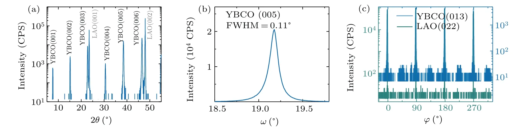
Fig.1.XRD characterization of high-quality YBa2Cu3O7−δ (YBCO)films deposited on LaAlO3 (LAO)substrates.(a)The θ–2θ diffraction pattern.Only(00l)peaks are observed for YBCO.(b)The rocking curve of YBCO(005)peak,showing a narrow full width at half maximum(FWHM)of 0.11.(c)The ϕ-scan result of YBCO(013)and LAO(022)peaks,both of which show clear four-fold symmetry.
3.2.DC characteristics
Temperature dependences of resistivity of the YBCO thin films with a thickness ranging from 400 nm to 1000 nm deposited under varying oxygen pressures from 0.25 Torr to 0.6 Torr have been measured.Figure 2 displays the temperature dependence of resistivity of a typical optimized YBCO film from 4 K to 150 K.The zero-resistance transition temperatureTc0is 92.1 K,and the difference betweenTc0andTc,onsetis less than 1 K.The black dashed line is the linear fitting of the normal state resistivity of the sample.The very small intercept at zero temperature confirms that few defects exist in the samples.However, no clear correlation was observed between zero-resistance transition temperature and either the film thickness or the deposition oxygen pressure.
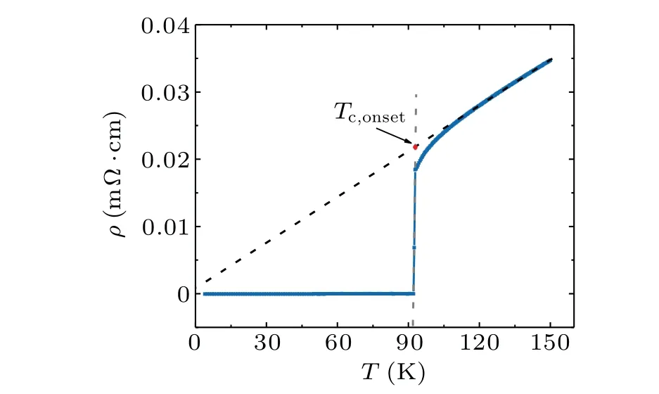
Fig.2.The temperature dependence of resistivity of a typical highquality YBa2Cu3O7−δ (YBCO)film.
3.3.Microwave properties and optimization
Surface resistances at 77 K of a series of YBCO films deposited on LAO substrates were obtained by the low temperature cavity described in Section 2.In contrast to the threshold thickness (>300 nm) and critical temperature, it is evident that the surface resistance is related to both the diamagnetism and oxygen pressures during the deposition process.
Figure 3 shows the surface resistance related to different zero-field-cooling (ZFC) magnetizations.TheRsvalue(T=77 K) of the YBCO films could be significantly optimized by increasing the laser pulse energy from 100 mJ to 280 mJ, resulting in a decrease in surface resistance from 60 mΩ to 1 mΩ, while the zero-field-cooling (ZFC) magnetizations increased by an order of magnitude.This could be explained by the superconducting volume fraction of the samples reflected by magnetizations.[30]
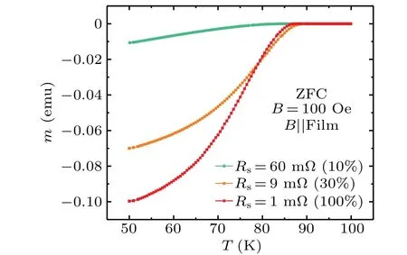
Fig.3.The microwave surface resistance(Rs)of YBCO films related to different zero-field-cooling(ZFC)magnetizations and superconducting volume fraction.
The superconducting volume fraction can be calculated using the equation
and the calculated results are shown in Fig.3.According to the London equations, the microwave surface resistance of a superconductor is caused by the normal state electron.Therefore,the YBCO thin films with a higher superconducting volume fraction have a lower normal electron content, resulting in smallerRsvalues.
Figure 4 shows the surface resistance results related to different oxygen pressures.It can be observed that theRs(T=77 K) reduces with the increase of the oxygen pressure from 0.25 Torr to 0.6 Torr.The film with the lowestRs(T=77 K)of 0.7 mΩ is shown in Fig.4(b).This result is comparable with theRs(T=77 K) of the commercial films such as DyBCO films made by CERACO.
To explain the observed result, it is easy to consider the effect of oxygen vacancy in the film due to the variation of oxygen pressure on the change inRs,so these films have been characterized by XRD.However, the XRD peak shifts were negligible with changes in oxygen pressure,leading to a conclusion that the change inRswas not caused by a change in oxygen content.Recently, the microstructure of YBCO films in a similar situation was measured,and it was suggested that the change in the microstructure of the film with changes in oxygen pressure may be responsible for the variation inRs.The relevant content has been published in Ref.[31].
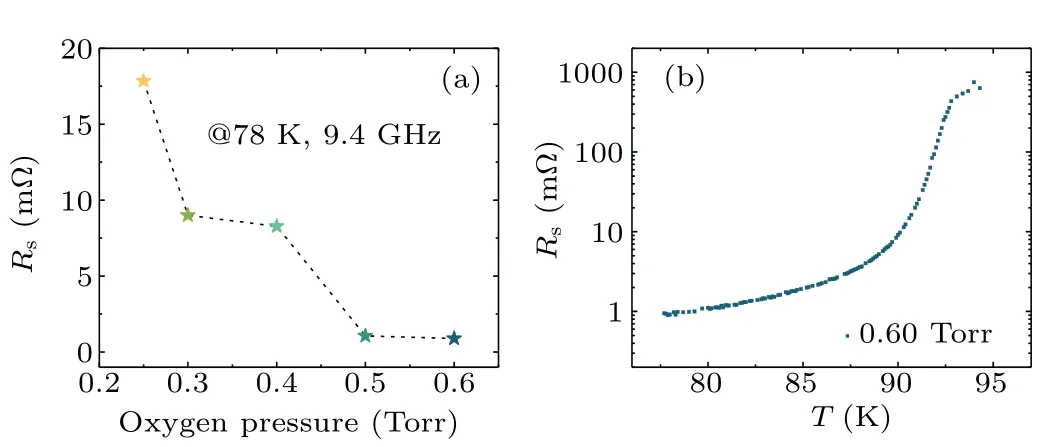
Fig.4.The microwave surface resistance (Rs) characterization of YBCO films deposited at different oxygen pressures.(a) The temperature dependence of the Rs of the YBCO films deposited at different oxygen pressures,measured at 9.4 GHz.(b) The relationship of Rs(T =77 K) of the YBCO films and their growth oxygen pressure.
3.4.Surface morphology
The presence of particle-like precipitates in high roughness YBCO thin films can cause problems in the fabrication of microwave devices such as electrode deposition and UV lithography.Therefore, the low roughness of the YBCO thin film is crucial for such devices.Figure 5 shows the SEM surface images of the YBCO films deposited in thicknesses of 50 nm, 300 nm and 1 µm.Figures 5(a)–5(c) show the surfaces of YBCO films deposited using target A with the compactness of 87%, while Figs.5(d)–5(f) show the surfaces of YBCO films deposited using target B with the compactness of 97%, the precipitates on the surface decrease when target B with a compactness of 97% is used.Evidently, the SEM images reveal that the presence of the precipitates on surface decreased when target B with the compactness of 97%was applied.However,the precipitates on the surface increased with the increase in film thickness.[32–35]Therefore,it can be concluded that improving the compactness of YBCO targets can greatly improve the surface morphology of films,meeting the requirement of subsequent fabricating processes.It is important to note that no correlation was observed between surface roughness and surface resistance in this study.
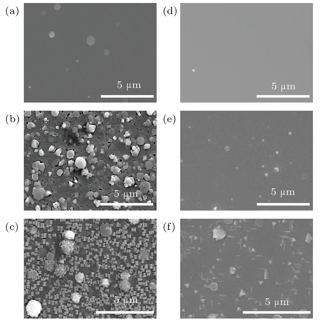
Fig.5.The surfaces of YBCO films with different thicknesses deposited using targets A and B,respectively.(a)–(c)The surfaces of YBCO films deposited using target A with thicknesses of 50 nm, 300 nm and 1 µm, respectively.(d)–(f)The surfaces of YBCO films deposited using target B with thicknesses of 50 nm,300 nm and 1µm,respectively.
3.5.Large-area uniformity
The distributions of thickness andRsof the 2-inch YBCO thin film for microwave application are shown in Figs.6 and 7, respectively.The thickness of the 2-inch YBCO thin film for microwave application exhibits 4% homogeneity within 15 mm,but decreases rapidly beyond this range from the center.Similarly,the surface resistance shown in Fig.7 is 0.7 mΩwith 1% homogeneity within 15 mm, but becomes unstable beyond this range from the center.

Fig.6.The thickness distribution of large-area YBCO film.
The distribution of critical current density in the 2-inch YBCO thin film for microwave application is shown in Fig.8.Within 15 cm from the center,a uniform distribution ofJcwas observed with the highest value of 1.6 MA/cm2.However,outside the 15 cm circle,a random distribution was found,which is consistent with the thickness and surface resistance results.
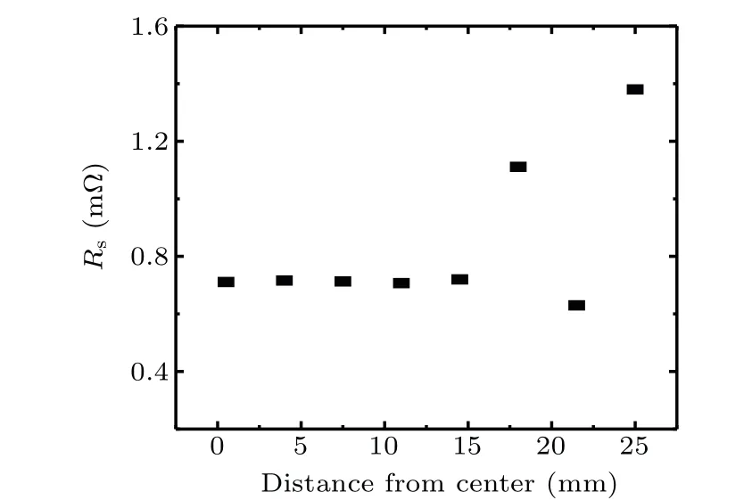
Fig.7.The Rs distribution of large-area YBCO film.

Fig.8.The Jc distribution of large-area YBCO film.
3.6.Application demonstration
To assess the practicability of the YBCO thin film in this work, 2-inch double-sided YBCO thin films were deposited,with one side patterned for a quasi-elliptic bandpass filter.The filter had a center frequency of 370 MHz and a bandwidth of 20 MHz.A filter with the same specifications was fabricated on a DyBCO thin film from CERACO for comparison.Both filters were measured at 87.8 K in a cryo-cooler by Agilent N5230A without tuning.The measured responses of the two filters are depicted in Fig.9(a), and the insertion losses are detailed in Fig.9(b).The transmission responses are well consistent, although there is a slight difference in bandwidth,which could be attributed to the different substrate thicknesses of these two films.Insertion losses of the two filters are at the same level,whereas the ripples are different due to the untuned reflection parameters.The result suggests that the YBCO films in this work could completely meet the requirements of microwave devices.
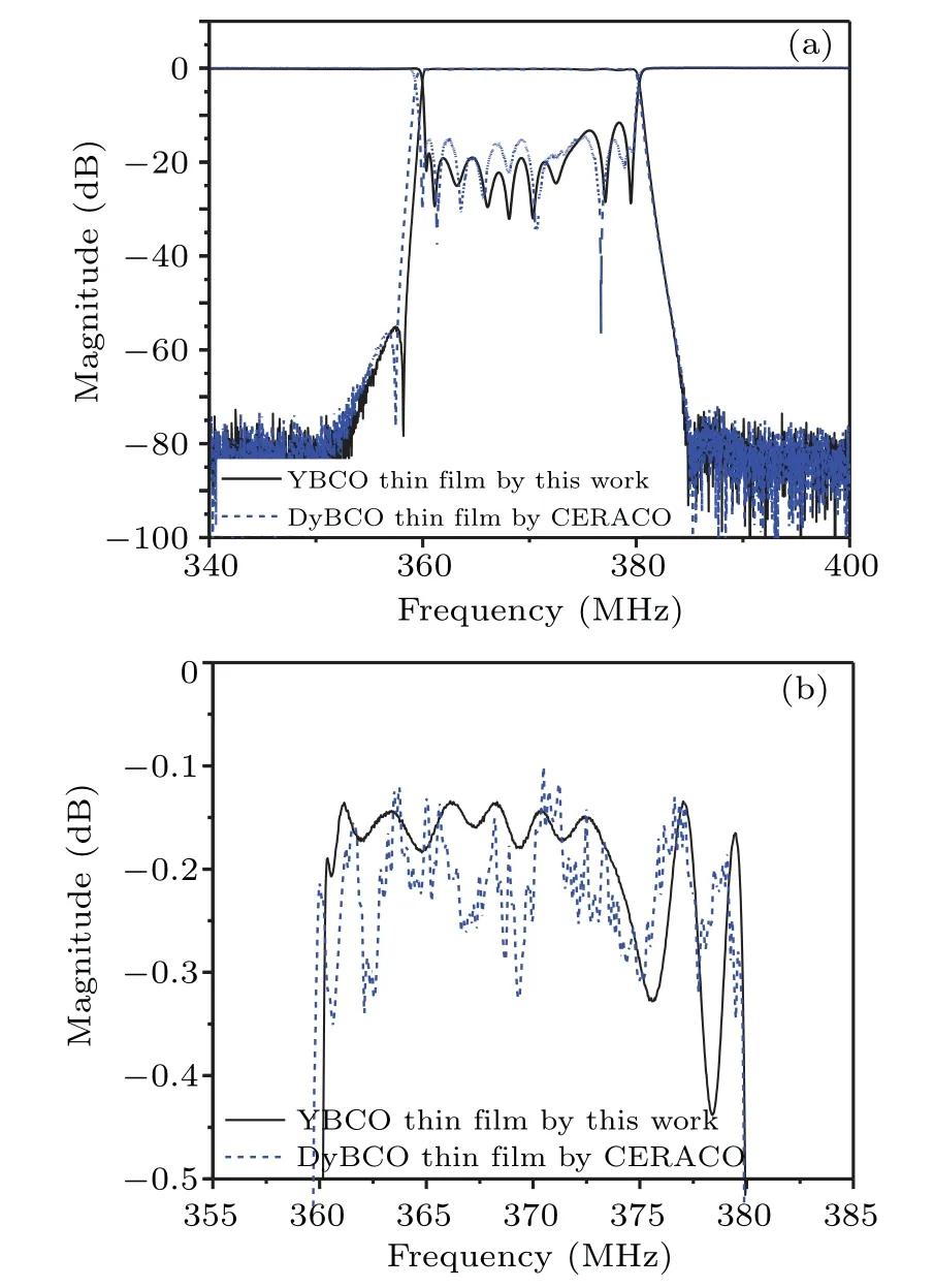
Fig.9.Comparison of filters fabricated on YBCO thin film in this work and DyBCO thin film from CERACO:(a)responses;(b)insertion losses.
4.Conclusion and perspectives
In this paper, the large-area YBCO films with (00l)-oriented,highTc,and high fraction of superconducting phase were successfully deposited by PLD.The results of theRsmeasurement inferred that increasing the laser pulse energy and the oxygen pressure during deposition can effectively reduce theRsof the film.The surface morphology of YBCO films can be improved by using a high-densification target.Large-area double-sided YBCO films were successfully deposited for superconducting filters.The comparison results indicate that the YBCO films in this work could completely meet the requirements of microwave devices.
Acknowledgements
Project supported by the National Key Basic Research Program of China (Grant Nos.2022YFA1603903 and 2021YFA0718700), the Key-Area Research and Development Program of Guangdong Province, China (Grant No.2020B0101340002), the National Natural Science Foundation of China(Grant Nos.61971415,51972012,11927808,119611410, 11961141008, and 12274439), the Strategic Priority Research Program(B)of Chinese Academy of Sciences(Grant No.XDB25000000),Beijing Natural Science Foundation(Grant No.Z190008),and Basic Research Youth Team of Chinese Academy of Sciences(Grant No.2022YSBR-048).
猜你喜欢
Chinese Physics B(2023年9期)2023-10-11 07:56:48
Chinese Physics B(2022年6期)2022-06-29 08:54:16
Chinese Physics B(2021年1期)2021-01-21 02:07:36
北方音乐(2019年10期)2019-07-10 19:13:36
中华建设(2019年5期)2019-07-05 07:44:36
北方音乐(2019年9期)2019-06-20 09:41:09
丝路艺术(2018年10期)2018-09-21 12:17:40
家庭百事通(2016年5期)2016-05-06 17:29:16
第二课堂(课外活动版)(2015年4期)2015-10-21 19:41:18
家庭医药(2004年10期)2004-04-29 15:42:14
- Chinese Physics B的其它文章
- First-principles calculations of high pressure and temperature properties of Fe7C3
- Monte Carlo calculation of the exposure of Chinese female astronauts to earth’s trapped radiation on board the Chinese Space Station
- Optimization of communication topology for persistent formation in case of communication faults
- Energy conversion materials for the space solar power station
- Stability of connected and automated vehicles platoon considering communications failures
- Lightweight and highly robust memristor-based hybrid neural networks for electroencephalogram signal processing