A micro-chip exploding foil initiator based on printed circuit board technology
Zhi Yang ,Peng Zhu ,* ,Qing-yun Chu ,Qiu Zhang ,Ke Wang ,Hao-tian Jian ,Rui-qi Shen
a School of Chemical Engineering,Nanjing University of Science and Technology,Nanjing,210094,China
b Micro-Nano Energetic Devices Key Laboratory,Ministry of Industry and Information Technology,Nanjing,210094,China
Keywords:Exploding foil initiator Printed circuit board Monolithic structure Firing validations
ABSTRACT Conventional exploding foil initiator(EFI)in ignition or detonation applications hosts many performance advantages,but was hindered by the bulky,inaccurate,inefficient and expensive shortcomings.We highlight a novel micro-chip exploding foil initiator(McEFI)using printed circuit board(PCB)technology.The structural parameters were determined based on energy coupling relationship at the component interfaces.Next,the prototype McEFI has been batch-fabricated using PCB technology,with a monolithic structure of 7.0 mm(l)×4.5 mm(w)×4.0 mm(δ).As expected,this PCB-McEFI illustrated the successful firing validations for explosives pellets.This paper has addressed the cost problem in both military munitions and civil markets wherever reliable,insensitive and timing-dependent ignition or detonation are involved.
1.Introduction
Explosive is a kind of energetic material with high energy density,which plays an important role in the progress of human civilization.How to realize its output with high safety and reliability is a practical problem that needs to be solved immediately.Exploding foil initiator(EFI),also known as slapper detonator,was first introduced by Stroud JR in 1976[1].EFI consists of a substrate,a bridge foil,a flyer layer,a barrel and an explosive pellet.When a desired short-duration pulse shock is met,EFI operates by accelerating a plastic flyer disk to a high velocity and then directing the flyer fragment into the output explosive[2-8].The impact induces a shock wave that causes combustion or detonation of the explosive pellet when fits the critical energy initiation criteria [9-11].This work mode ensures the excellent shot to shot repeatability compared with counterparts [12].Another merit of EFI is that the bridge foil and explosive pellet are physically separated by a thin insulating material and an air gap.This contributes to safety because unintentionally current signals from such as electromagnetic interference or electrostatic discharge have no access to accidents.
Components are individually hand-placed to construct a single assembly of conventional EFI,which results in disadvantages of bulky,inaccuracy,inefficient,and expensive.Therefore,after EFI was proposed microelectronic fabrication technique had been adopted to the fabrication of EFI in order to realize miniaturization,integration,mass-production,and low-cost [13,14].However,such EFI structures cannot be assured to resist impact-load under harsh environments,due to the fragile substrate materials [15,16].In addition,there were multi-steps in the fabrication process [17],which reduced the efficiency.As a result,the high price still remains [18],impeding the widespread utilization of EFI.
Printed circuit board (PCB) is an established and promising technology capable of mass-producing electric circuits at low cost.The modular integration of electromechanical components and functions can be supported,because PCB technology provides the opportunity between electronic elements and electrical connections.Especially the PCB process is suitable for the production of multi-layer boards,which ensures the increased design flexibility,reduced device volume,and improved automation level.It will certainly overturn the fabrication idea if this radical process be adopted to develop an EFI.
This paper discusses the design,fabrication and characterization of a low-cost micro-chip exploding foil initiator(McEFI)using PCB technology.The structural parameters were developed applying simulation and modeling on its components.The novel McEFI was monolithic,and had an overall size of 7.0 mm (l) × 4.5 mm(w)×4.0 mm(δ).The prototype configuration was examined by the micro-computed tomography (μCT),which indicated that the PCB technology meet the requirements of machining accuracy.Furthermore,the primary characteristics of PCB-McEFI were performed and discussed,including the electrical-explosion properties and initiation capabilities.This revolutionary innovation of preparation process truly implements the popularization of McEFI with impact-load resistance and negligible cost,and allows for the direct integration into the discharging circuit.
2.Design,simulation and modeling
2.1.Electro-thermal simulation of Cu bridge foil
A high-voltage is typically applied across two contacts (also called pads) at the ends of the bow-tie region,which introduces a proportionately large current density in the necked-down portion(bridge foil).According to the working principle of EFI,the metal bridge foil plays the role of converting the electric energy stored in the capacitor into the kinetic energy of the flyer,thus it is expected to be heated uniformly and exploded simultaneously.Therefore,an electro-thermal analysis was first conducted with the solution of the transient heat conduction equation [19],

where cis the specific heat capacity of Cu at constant volume,J/(kg.K);ρis the density,kg/m;T is the temperature,K;t is the time,s;σis the electrical conductivity,S/m;E is the electrical field intensity,V/m;and λis the heat conductivity,W/(m.K).
Furthermore,the heat capacity,electrical conductivity,and heat conductivity are all related to the temperature,and can be described empirically as follows,

The electro-thermal process should obey the current continuity equation,

where J is the current density,A/m.
Assuming the current across the bridge foil rises to 3000 A within 100 ns,it can be simplified to a sinusoid,as

The heat exchange between the bridge foil and the environment is ignored in such a short period of time,that is,electro-thermal action is calculated in an adiabatic process.Electro-thermal analysis of the bridge foil was performed by COMSOL Multiphysics 5.3 program to exhibit temperature gradient distribution before melting point(1358 K).
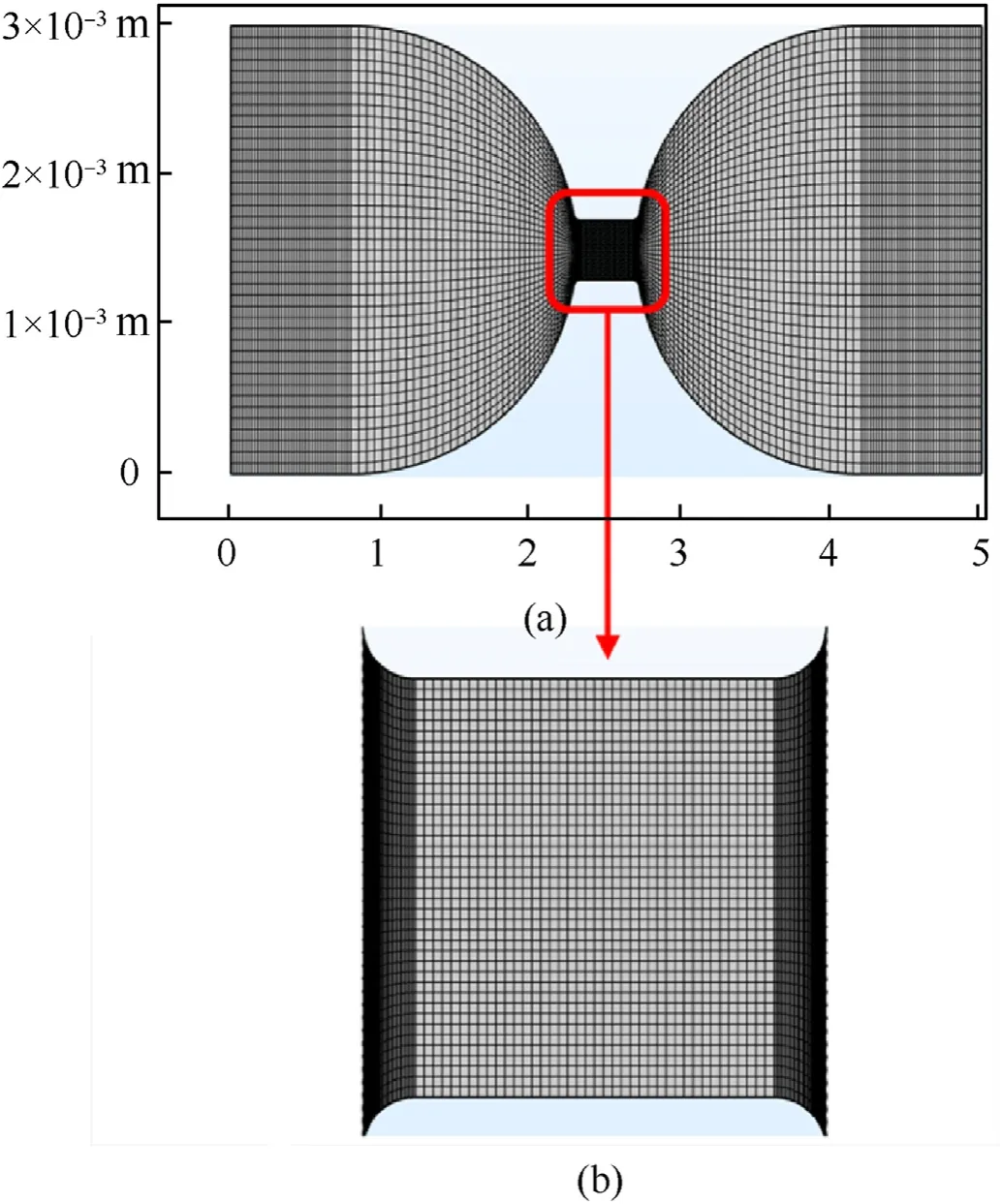
Fig.1.(a) Mesh generation of the model;(b) zoom in detail of the Cu bridge foil.
Fig.1 shows the mesh generation of the model and the zoom in detail of bridge foil with sectional size of 400 μm(l)×400 μm(w).When the sectional size is fixed,the thickness of bridge foil is the only determinant that directly affects the endothermic melting reaction by adjusting the resistance value.There is skin effect in high frequency circuit.The skin-effect depth can be calculated by combining the angular frequency of current(ω=1.57×10rad/s)with the magnetic permeability(μ=4π×10H/m)and electrical conductivity of Cu (σ).According to equation (2),the maximum conductivity of Cu is 6.00 × 10S/m at 298.15 K,so the minimum skin-effect depth of 41 μm is obtained.The skin effect of current can be neglected because the minimum depth is large than the foil thickness.
It was evaluated that the melting time of Cu bridge foil with thicknesses varying from 1 μm to 9 μm,and Fig.2 shows the simulation results under the action of instantaneously large pulse current of 3.00 kA/100 ns.First,when the thickness is larger than 5 μm,the melting point lags behind the risetime to the peak current,which is unfavorable to make the electrical-explosion come true.On the other hand,the foil size should be adequate to ensure the enough output pressure generated from gases and plasma during the electrical-explosion.Accordingly,the right thickness of 5 μm has been ascertained,and the size of bridge foil has been set as 400 μm (l) × 400 μm (w) × 5 μm (δ).
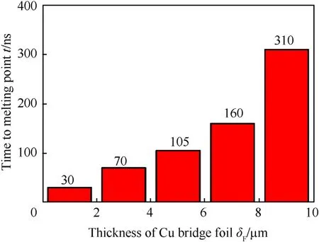
Fig.2.Melting time of Cu bridge foil with thicknesses varying from 1 μm to 9 μm.
Fig.3 shows the electro-thermal coupling results at different times ranging from 40 ns to 110 ns,where Fig.3(a)illustrates there is a tiny rise in temperature emerging at four corners at 40 ns.As current flow continues in time,the temperature gradually rises in the middle of the foil,and spreads into the surrounding areas.The global temperature rises faster and faster,finally reaches the melting point at about 105 ns,locating between Fig.3(e) and (f).Consequently,the main body is heated almost-uniformly with a very small melting time difference,which predicts the Cu bridge foil burst almost-synchronously.With the increase of the current rising rate,the time to reach melting point is shortened and the difference is reduced,which is more conducive to the simultaneous electrical-explosion.
2.2.Calculation of FR-4 flyer shock pressure and duration
PCB substrate generally refers to the copper clad laminate,and one can obtain the desired circuit patterns or mechanical structureson the substrate.FR-4 is one of the most common PCB substrates,whose base material consists of epoxy resin and fiber-glass cloth.In order to improve the manufacturing efficiency and the prototype integration,FR-4 was directly selected as the flyer material in this work.The thickness of FR-4 flyer was set as 75 μm limited by the drilling precision of PCB approach.First,the terminal velocity of FR-4 flyer was calculated using the electrical gurney energy model[20],

where vis the terminal velocity,m/s;k and n are two constants related to bridge foil material;R is the mass ratio of flyer to bridge foil per unit area;and Jis the burst current density,A/cm.
R can be solved with the following equation:

where ρand ρare the densities,g/cm;δand δare the thicknesses of flyer and bridge foil respectively,μm.
When the parameters of Cu bridge foil and FR-4 flyer were determined,vdepended only on the J,

where Iis the burst current,A;S is the cross-sectional area,cm.
The material properties used for the calculation of flyer velocity are shown in Table 1.Assuming the burst current is 2.25 kA,the calculated burst current density is 1.13 × 10A/cm,then the terminal velocity of 1907 m/s can be figured out.

Table 1.Material properties for the terminal flyer velocity.
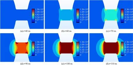
Fig.3.Electro-thermal simulation results of Cu bridge foil.
Next,we evaluate the shock pressure of FR-4 flyer imparting to explosive of HNS-IV (Hexanitrostilbene,[CH(NO)CH]) pellet[22,23],

where pis the shock pressure of flyer imparting to explosive,GPa;ρis the density of explosive pellet,g/cm;Dis the shock wave velocity in the pellet,m/s;and uis the particle velocity of explosive,m/s.
There is a linear relationship between the shock wave velocity and the particle velocity:

where cand λare Hugoniot coefficients of the explosive.
Consequently,the shock pressure can be derived using (8) and(9):

According to Newton's third law of motion,the flyer will be subject to the reaction force from the explosive pellet:

similarly where pis the shock pressure of the explosive pellet on the flyer,ρis the density of flyer,Dis the shock wave velocity in the flyer,uis the particle velocity of flyer,and vis the terminal flyer velocity calculated by Eqs.(5)-(7).
There is also a linear relationship between Dand u:

similarly where cand λare Hugoniot coefficients of the flyer.
The shock pressure is acquired with (11) and (12):

Both the particle velocity and the shock pressure are continuous at the impact interface,that is

Accordingly,the particle velocity and the shock pressure can be obtained using Eqs.(10),(13) and (14).
A shock wave emerges in the FR-4 flyer,because the shock impedance (ρD) of HNS-IV pellet is larger than that of the flyer.Subsequently a rarefaction wave is reflected when the shock wave arrives at the free surface of flyer.The shock duration is the time before the rarefaction wave catches up the shock wave,thus the shock duration is calculated with the FR-4 flyer thickness,

The shock wave velocities and particle velocities of a fiber-glass reinforced polyester were given in the reference [24],so the approximate Hugoniot coefficients of FR-4 flyer were obtained bylinear fitting with these data.Coefficients for the calculation of shock pressure and shock duration are listed in Table 2.

Table 2.Material properties for the shock pressure and shock duration.
The calculated shock pressure and shock duration were 6.26 GPa and 39.82 ns,respectively,corresponding to the calculated velocity of 1907 m/s.It is indicated that PCB-McEFI is feasible to detonate the HNS-IV pellets due to such high shock pressure and duration,compared with the reference results[25-27].
2.3.Determination of FR-4 barrel dimension
The barrel is another key component in the McEFI,which plays three main roles:(1)shearing the FR-4 film into flyer;(2)providing the accelerating distance for FR-4 flyer;(3)alleviating the influence of rarefaction wave on the shock pressure.This demands the barrel should be provided with sharp edge and good perpendicularity,so materials such as sapphire,stainless steel,silicon and SU-8 photoresist have been widely utilized in the previous study.However,these barrel materials are not conducive to realize batchpreparation of McEFI via PCB technology.In this work,FR-4 was directly worked as barrel,simplifying the preparation processes.
The diameter (φ) of FR-4 barrel should be capable of involving the electrical-explosion area,which is usually determined by the side length of bridge foil.When φ is set as 600 μm,the melting zone of bridge foil is exactly covered by the barrel according to the electro-thermal simulation results in section 2.1,which is advantageous to make the most of electrical-explosion energy.The theoretical height (δ) of FR-4 barrel is corresponding to the value where flyer reaches its peak velocity,which is conducive to the impact of flyer on explosive pellet.In our previous work [15],we adopted the ceramic flyer with 50 μm thickness,whose mass is almost the same as 75 μm-thick FR-4 flyer.Hence,we set the same height as 400 μm in this work.
The FR-4 substrate,also called reflector,should has enough hardness or stiffness to avoid deformation,aiming to completely reflect the electric explosion.Accordingly,the FR-4 substrate was thickened compared with the conventional silicon or ceramic materials,and its thickness was 2.0 mm.The length and width of the substrate depend on the size of bridge foil,and to be set as 7.0 mm(l)×4.5 mm(w).In summary,the structural parameters of PCB-McEFI are listed in Table 3.

Table 3.Structural parameters of PCB-McEFI.
3.Experimental setup
3.1.Fabrication of PCB-McEFI
PCB technology with multilayer boards refers to the technology that multiple PCBs (single-sided or double-sided copper clad laminates) were laminated together with pressure attributing to the bonding effect of heating prepregs (PP).Fig.4(a) shows the McEFI was batch-fabricated by laminating two PCBs,where PCB-1and PCB-2 had the same overall size of 7.0 mm (l) × 4.5 mm(w) × 2.0 mm (δ).
Unlike multi-steps are required to prepare each component in our previous work[17],in this work PCB technology can realize the integrated preparation of McEFI.There were six detailed steps to manufacture PCB-McEFI.(1) PCB-1 with double-sided copper ofabout 12 μm-thickness was first obtained using electroplating technology,then the Cu foil was reduced to about 5 μm in the acid cupric chloride(CuCl)etchant with a certain concentration.(2)Cu bridge foil was acquired on the Top layer of PCB-1 (L3),based on photolithographic masking and etching approaches.The photolithographic masking processes played the role of pattern transfer from an ultraviolet-sensitive dry film to the Cu surface,which consisted of main procedures of coating,exposure and developing.Other undesirable Cu that was not protected with dry film would be etched in the CuCletchant.(3) PCB-1 and PCB-2 were pressedlaminated with the bonding effect of a 25 μm-thick PP.(4) In order to introduce the large pulse current into the bridge foil,viaholes (plating-holes) passing through two pads were fabricated using plated-through-hole technology after mechanical drilling.(5)Two rectangular Cu pads coating with electroless nickel immersion gold,were prepared on the Bottom layer of PCB-1 (L4),which facilitate the electrical connection with surface mounted technology.(6) From the Top layer of PCB-2 (L1),the FR-4 barrel was formed by drilling the PCB-2 up to the reserved flyer layer,and the height of barrel was 400 μm.Due to the FR-4 board and PP had the same main material of fiber-glass,the height of FR-4 flyer was 75 μm consisting of 50 μm-thick FR-4 board and 25 μm-thick PP.A larger hole was drilled with diameter of 2.4 mm,which worked as a shell for the explosive pellet.As a result,Fig.4(b) shows the photograph of PCB-McEFI,with an overall dimension of 7.0 mm (l) × 4.5 mm (w) × 4.0 mm (δ).
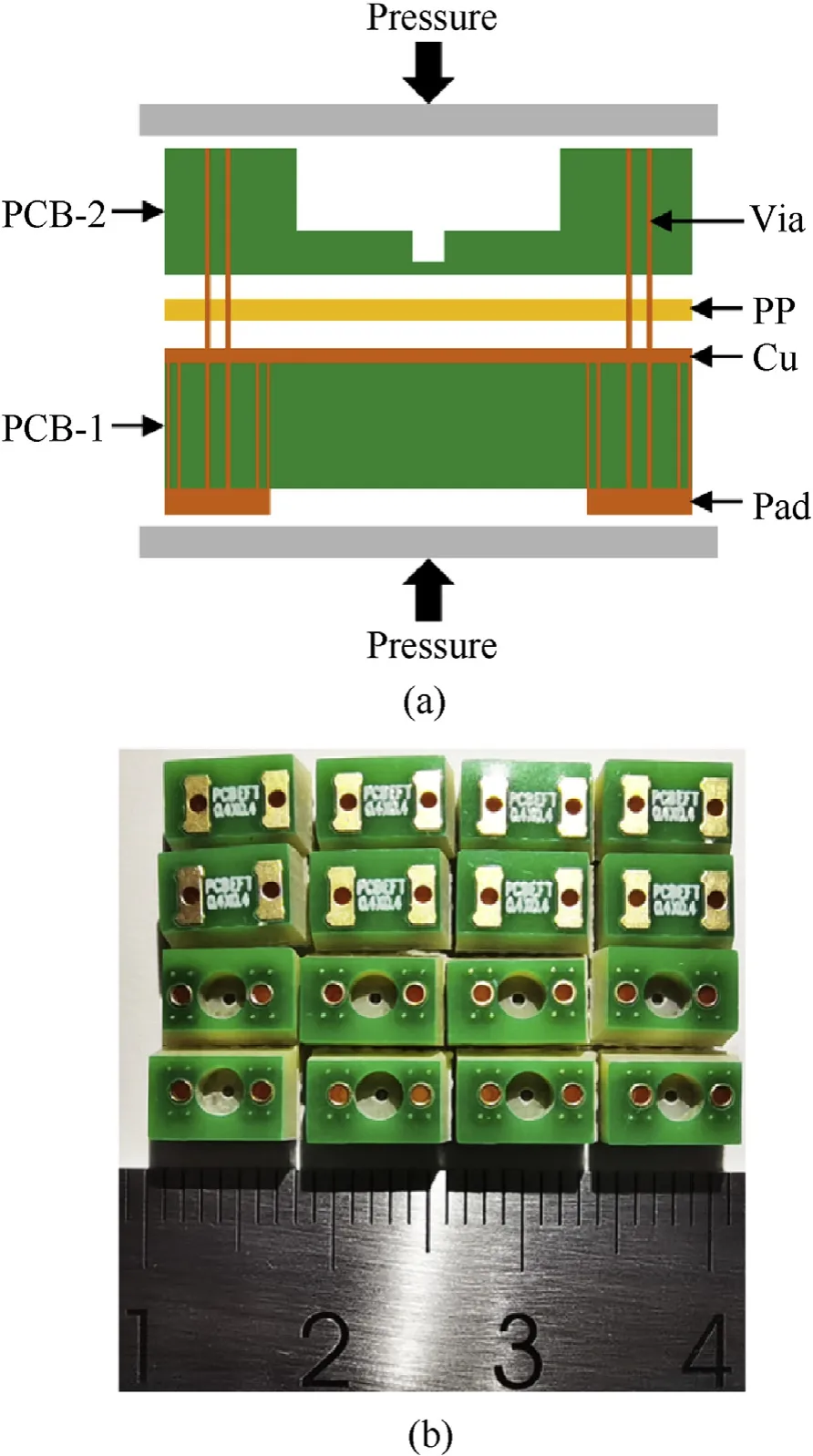
Fig.4.(a) PCB laminating process for the fabrication;(b) photograph of PCB-McEFI.
3.2.Configuration examination of prototype
A μCT can reconstruct the 3D(three dimensional)and sectional appearances of an objective down to microscale.The internal structure of the PCB-McEFI could not be photographed using a traditional optical camera due to the existence of the cover board(PCB-2),thus its 3D morphology was reproduced with μCT technique.
3.3.Primary characteristics of PCB-McEFI
The electrical-explosion means the process of metal bridge foil is exploded by the large pulse current from a high-voltage capacitor.This complex process made the energy conversion that benefited from a phase transition from solid to liquid,liquid to gas,then to plasma.Fig.5 shows the schematic diagram of discharging circuit for Cu bridge foil,including high-voltage capacitor,pulse power switch,bridge foil,and circuit connections.The lumped resistance(R)and lumped inductance(L)of the discharging circuit were about 140 mΩ and 40 nH,respectively.
The voltage signal across the bridge foil was obtained with a high-voltage probe (Teledyne LeCroy HVD3605A),and the circuit current was monitored by a Rogowski coil (CWTUM/30/R with a sensitivity of 1 V/kA).These two waveforms were recorded using a digital storage oscilloscope(LeCroy WR 104Xi-A with a bandwidth of 1 GHz,at a sampling rate of 10 Gs/s),and other electrical parameters can be acquired with them.In this paper,the electrical parameters were determined under discharging voltages varying from 1.25 kV to 2.00 kV (the capacitance were 0.22 μF or 0.40 μF),including the peak current,peak voltage,peak current time,burst time,burst current,burst power,burst energy,and energy deposition ratio.
Ultra-high-speed photography has been widely popular among fluids experiments,which provides with precise information of the event through capturing a sequence of video frames with high temporal and spatial resolution.In order to give a complete visualization of explosion,the flow field of bridge foil was observed via an ultra-high-speed framing camera (SIM X,belongs to the Specialised Imaging Ltd).This real-world measurement supplemented the details to understand the electrical-explosion history from the starting of capacitor discharging.At last,the prototype PCB-McEFI was utilized to directly check the firing properties of explosives,consisting of the shock ignition of BPN (the mixture of boron and potassium nitrate,B/KNO) and the shock detonation of HNS-IV.
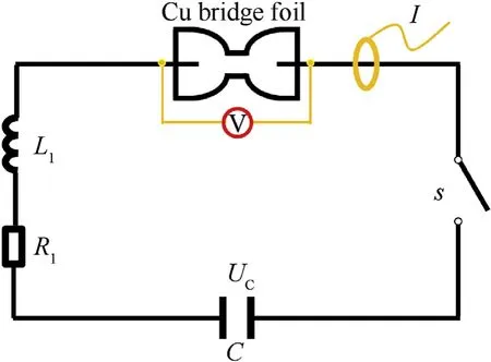
Fig.5.Schematic diagram of the discharging circuit for Cu bridge foil.

Fig.6.Cu bridge foil morphology of 2D (a) and 3D (b) via laser confocal microscopy.
4.Results and discussion
4.1.Configuration by advanced optical photography
Fig.6 shows the construction of Cu bridge foil via laser confocal microscopy,whose 2D and 3D appearances are presented in Fig.6(a) and (b),respectively.In Fig.6(a),the length and width of bridge foil were 405 μm and 397 μm,respectively,which fit the designed parameters.Therefore,photolithographic masking and etching processes could meet the requirements of precise pattern of bridge foil.Furthermore,the electrodeposited Cu foil had a rather coarse surface presented in Fig.6(b),and the average thickness was 4.9 μm.
Fig.7(a) shows the 3D configuration,including the detailed geometries,as well as the relative positions of the bridge foil,barrel,vias,pads,and explosive casing.This constructional detail was consistent with the prototype,as presented in the upper-left corner.Fig.7(b) shows the top view,located in the inner layer(L3).There were ten plating-holes to realize electrical conduction,consisting of eight smaller blind-vias with 300 μm diameter and two larger through-vias with 800 μm diameter.Fig.7(c) shows a cross-sectional structure,along the center and perpendicular to YOZ plane.The two through-vias passing through the two pads were clearly delineated,and the barrel size was 600 μm(φ)×400 μm(δ).In summary,these marked structural parameters were basically consistent with those in Table 3,indicating PCB processes could meet the precision requirements for the McEFI fabrication.
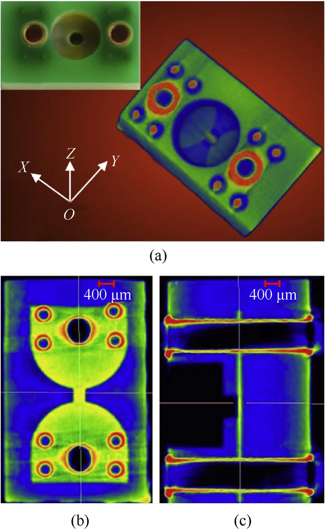
Fig.7.Scanning image of PCB-McEFI via μCT of(a)3D tomography,(b)top view and(c)sectional configuration.
4.2.Electrical-explosion characterizations
4.2.1.Electrical parameters of bridge foil
The electrical parameters of Cu bridge foil are listed in Table 4,under capacitor discharging voltages ranging from 1.25 kV to 2.00 kV (the capacitances were 0.22 μF or 0.40 μF).The burst time refers to the moment where the power calculated by voltage multiply current climbs up to climax,which is found almost to be in line with the time of voltage spike.At this time,the bridge foil has been vaporized,and we can figure out the burst current,burst power,and burst energy (the integral of power over time).The energy deposition ratio indicates how much energy stored in the high-voltage capacitor was transferred into the bridge foil,which was calculated with the burst energy divided by the storage energy.

Table 4.Electrical parameters of Cu bridge foil.
As the step-up of discharging voltages,the peak current,peak voltage,burst current,burst power,and burst energy were all increased under the identical high-voltage capacitor.Furthermore,the peak current time and burst time presented an approachingtendency with the increase of voltages from 1.25 kV to 2.00 kV,which is conducive to enhance the burst current and the final velocity.The energy deposition ratios were at a rather low level,ranging from 19.9% to 25.1%,with a mean value of 23.0%.We hold the reason was the thick foil and the rather coarse surface,which was disadvantageous to introduce a good electrical-explosion[28,29].
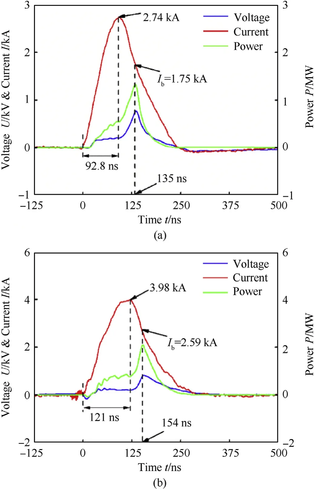
Fig.8.Typical discharging curves at conditions of 0.22 μF/1.50 kV (a) and 0.40 μF/1.50 kV (b).
Fig.8(a)shows the typical discharging curves at the state of 0.22 μF/1.50 kV,which plots the instantly large pulse current with peak value of 2.74 kA after the risetime of 92.8 ns.The burst time of bridge foil was 135 ns,so its vaporization time was 20.0 ns,which was the subtraction result by deducting the melting time of about 115 ns from the electro-thermal simulation.The results show that once the current flowed through the bridge foil,the temperature rise rate would be higher and higher,which was consistent with the electro-thermal simulation.The burst current was 2.59 kA when the Cu bridge foil operated under 0.40 μF/1.50 kV,as plotted in Fig.8(b).Therefore,HNS-IV pellets can be theoretically reliablyinitiated by this firing condition according to the calculated shock pressure and duration in section 2.2.
4.2.2.Explosion flow field of bridge foil
Fig.9 shows the photographic images for the blast flow field of Cu bridge foil at 0.22 μF/1.50 kV,via the ultra-high-speed framing camera of SIM X.The interval between two adjoining pictures was kept as 20 ns with 5 ns exposure.The first photo was acquired before burst point,so it was regarded as initial time point,the next pictures were recorded in sequence with 20 ns interval.The electrical-explosion phenomenon took the lead at the corners,which was consistent with the electro-thermal simulation.This also illustrates the rational design of the 600 μm diameter of FR-4 barrel,because the whole explosion zone of bridge foil is completely involved by the barrel,so as to make the best of electrical-explosion energy.The explosion took place within 40 ns from the initial moment,and the width of explosion flow field at 60 ns was about twice as original foil width due to the adjacent areas were affected.After that,the explosion was gradually weakened and the field was shadowed with the dissipation of gases and plasma.A large amount gases and plasma with high-temperature and high-pressure were generated after the electrical-explosion,which further boosted the FR-4 flyer in the FR-4 barrel.
4.3.Firing validation
4.3.1.Shock ignition of BPN
Fig.10(a)shows the capacitor discharging unit(CDU)for firing validation.This CDU was a series circuit,including a high-voltage capacitor (located on the back of testing PCB),a PCB-PTS (planar triggered spark-gap switch) [30],and a PCB-McEFI.Fig.10(b) illustrates the operation of shock ignition.Cu bridge foil was exploded into gases,plasma and shock waves,to shear and drive the FR-4 flyer inside the FR-4 barrel,finally high-speed flyer out of the barrel impacted the pellet to realize firing output.The experiment results show that BPN pellets with size of 2.3 mm(φ)×2.0 mm(H)were ignited under the minimum firing condition of 0.22 μF/1.50 kV.Fig.10(c)shows the image frames of BPN flame recorded using high-speed photography.The ignition and combustion period with 249 ms could be divided into three stages,including the heating stage with a faint spot,the growth stage with bright spark that grew to its maximum within 15 ms,and the extinction stage as the combustion ended.
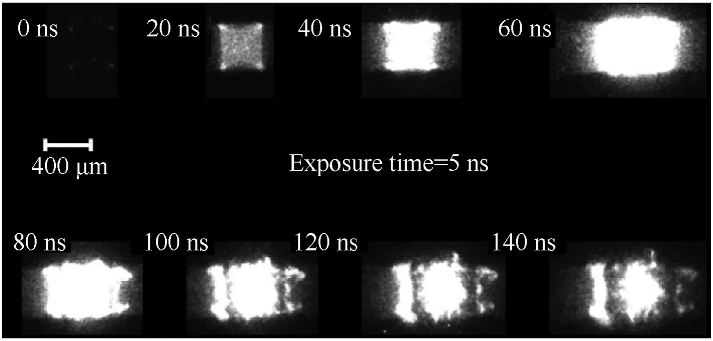
Fig.9.Explosion flow field of Cu bridge foil via an ultra-high-speed framing camera.
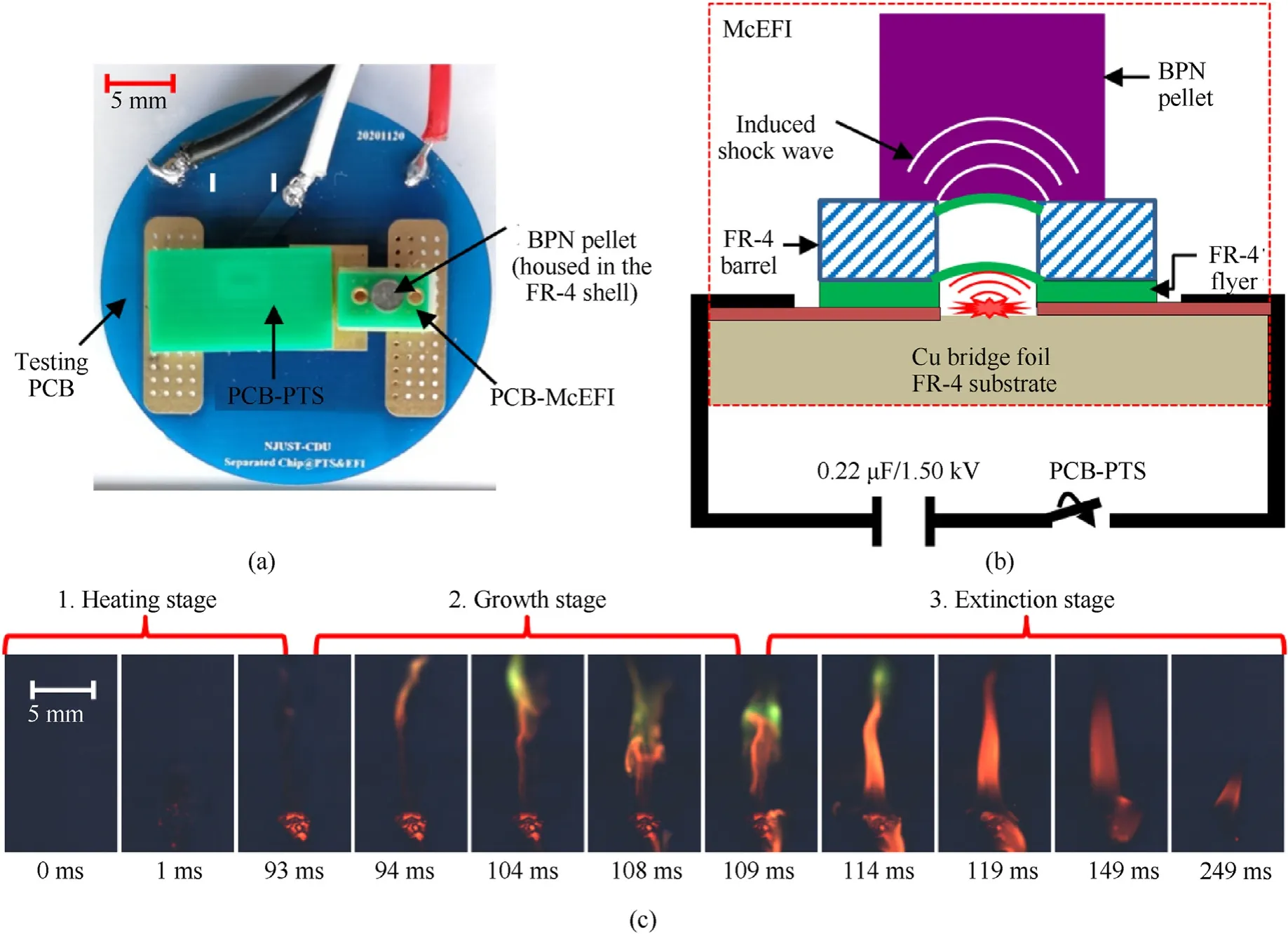
Fig.10.Shock ignition of BPN.(a) CDU for firing validation.(b) Operation of shock ignition.(c) Images of BPN flame via high-speed photography at 0.22 μF/1.50 kV.
4.3.2.Shock detonation of HNS-IV
EFI is also frequently adopted to realize the shock-to-detonation transition of explosives,and HNS-IV is a well characterized explosive that has been utilized in EFI for several decades[31-33].This is due to its reliable threshold energy to short-duration pulse shock under high-speed impact with small-size thin flyer plates,and its excellent thermal and shock stabilities.
Fig.11 shows the SEM(scanning electron microscope)image of HNS-IV powder,which was prepared via a homemade microfluidic platform with inherent safety and high throughput [34].The average particle size of HNS-IV was about 200 nm,so the calculated SSA was about 17 m/g[35],which fitted the specification.HNS-IV pellets were die-pressed in a mould to the dimension of 2.3 mm(φ)×2.0 mm(δ)with the density of 1.60 g/cm,as presented in the upper-right corner of Fig.11.By replacing the BPN pellet in Fig.10(a) with HNS-IV pellet,the shock results illustrated that explosive pellets were detonated under the minimum firing state of 0.40 μF/1.80 kV.
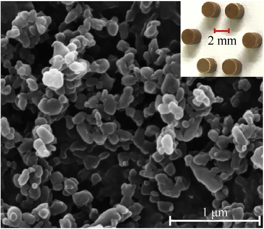
Fig.11.SEM image of HNS-IV and its pellets.
The burst current was 3.33 kA at 0.40 μF/1.80 kV,so we could figure out the burst current density as J=1.67× 10A/cm,further get the terminal velocity v=2403 m/s.The real velocity was higher than the threshold velocity of 1907 m/s,with a relative deviation of 26.0%.The reasons for higher firing energy were many aspects-involved,and we hold the first determinant was the heterogeneous foil surface that causing a low energy utilization ratio.Another main reason was that FR-4 flyer needed higher energy to shear,so that less energy was reserved for driving.
It was performed with numerical simulation that the shock-todetonation transition of HNS-IV pellet under the FR-4 flyer impact,in order to further check the higher firing energy compared with our previous work[15,16].The FR-4 flyer was described with shock equation of state(EOS).The Lee-Tarver ignition and growth model was arranged to describe HNS-IV,including two JWL (Jones-Wilkins-Lee) EOS and a three-term reaction rate equation.
The JWL EOS used for unreacted explosive and reaction products:

where p is pressure,v is relative volume,ω is the Grüneisen coefficient,cis the average heat capacity,T is temperature.A,B,Rand Rare all constants.
The three-term reaction rate equation used for HNS-IV pellet:

where λ is the reaction fraction,t is the reaction time,ρ is the current density,ρis the initial density,p is pressure.I,G,G,a,b,x,c,d,y,e,g and z are all constants.
The material properties of FR-4 were listed in Table 2,and Lee-Tarver model parameters were provided with the reference [27].ANSYS/AUTODYN was adopted to simulate the shock-to-detonation transition(SDT)process,and we obtained the threshold velocity of 2100 m/s after variable-step attempts.
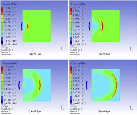
Fig.12.Pressure distribution among HNS-IV under the 2100 m/s threshold velocity.
Fig.12 shows the pressure distribution in HNS-IV pellet at different reaction moments,under the 2100 m/s threshold velocity of FR-4 flyer.The pressure increases exponentially with time,and the maximum pressure of about 22 GPa occurs at 0.4 μs.The explosive can produce steady detonation due to the pressure exceeds the Chapman-Jouguet pressure.It can be seen that the threshold velocity given by the simulation results is between the theoretical threshold (1907 m/s) and the practical initiation velocity (2403 m/s),which indicates the numerical simulation offers guidance to the following optimization.
5.Conclusion
In summary,we present a novel monolithic McEFI using PCB technology.The structural parameters were established,according to the electro-thermal simulation result of Cu bridge foil and the FR-4 flyer modeling relating to shock pressure and duration.The prototype McEFI has been batch-prepared based on PCB technology,including electroplating,photolithographic masking,etching,laminating,and drilling processes.Importantly,the firing properties of PCB-McEFI were tested by initiating BPN and HNS-IV pellets.The reason for high initiation energy has been explained qualitatively,and the SDT simulation has been performed with ignition and growth model.In the future,the structure matching design should be further performed to improve the energy utilization and firing sensitivity.
The authors declare that they have no known competing financial interests or personal relationships that could have appeared to influence the work reported in this paper.
We gratefully acknowledge the support from National Natural Science Foundation of China (Grant No.22075145).
- Defence Technology的其它文章
- Experimental study on propagation characteristics of rotating detonation wave with kerosene fuel-rich gas
- Adaptive robust control for triple avoidance -striking -arrival performance of uncertain tank mechanical systems
- Experimental study on WFeNiMo high-entropy alloy projectile penetrating semi-infinite steel target
- Numerical investigation of a muzzle multiphase flow field using two underwater launch methods
- Shock wave and bubble characteristics of underwater array explosion of charges
- On the higher-order thermal vibrations of FG saturated porous cylindrical micro-shells integrated with nanocomposite skins in viscoelastic medium

