
Anisotropic refraction and valley-spin-dependent anomalous Klein tunneling in a 1T′-MoS2-based p–n junction
2022-08-01 05:59:18FenghuaQi戚凤华andXingfeiZhou周兴飞
Chinese Physics B 2022年7期
Fenghua Qi(戚凤华) and Xingfei Zhou(周兴飞)
1School of Electronic Engineering,Nanjing Xiaozhuang University,Nanjing 211171,China
2New Energy Technology Engineering Laboratory of Jiangsu Province,School of Science,Nanjing University of Posts and Telecommunications,Nanjing 210023,China
Keywords: 1T′-MoS2,anisotropic refraction,valley splitting,Klein tunneling
1. Introduction
The discovery of two-dimensional transition metal dichalcogenides,[1](TMDCs, the generalized formula MX2with M=Mo, W and X=S, Se, Te) provides a highly practical and prospective platform for studying energy storage,[2]next-generation electronics and photonics,[3,4]novel topological electronic devices,[5,6]and heterostructure.[7]TMDCs monolayer has three typical structures, i.e., 2H, 1T, and 1T′structures.[6,8,9]Noticeably,1T′-MX2was predicted to possess tilted Dirac band structure by first-principles calculations[6]and has been prepared in experiment,[10–13]which distinguishes from the band structure of 2H and 1T structures (untilted Dirac band structure).Generally, compared with an untilted system, the tilted system shows a wide range of extraordinary properties, such as anisotropic plasmons,[14]anisotropic optical conductivity,[15]anomalous Klein tunneling,[16–20]and anomalous Andreev reflection.[21]Therefore, the tilted Dirac band structure of 1T′-MX2also attracts researchers to find unusual physical properties, e.g.,anisotropic longitudinal optical conductivities in 1T′-MoS2monolayer.[22]Here, we focus on the valley-dependent transport properties of electron in a 1T′-MoS2-based p–n junction.
Electrons in some materials can occupy some separated low energy states called valley in the momentum space. The earliest concept of valley degree of freedom can trace back to 1970s.[23,24]At the beginning of 21th century, valley-dependent physical properties were discussed in some traditional materials such as silicon[25]and AlAs quantum wells.[26]The concept of valleytronics, being similar to charge-based electronics and spin-based spintronics,emerged in graphene based on the manipulation of valley degree of freedom.[27,28]After that,a variety of Dirac materials,e.g.,silicene,[29]TMDCs monolayer,[30,31]and borophene,[32]were predicted to provide an important platform for realizing valleytronic devices such as valley filter,[27,33–35]valley valve,[36–38]and valley splitter.[39,40]The generation of valley polarization is a key factor for valleytronics applications. Traditionally,valley polarization is nonexistent in Dirac materials due to the valley degeneracy and hence the method of applying external fields,e.g.,electric field,light illumination,and strain,is an efficient method to generate valley polarization.[41–47]In this paper,owing to the anisotropic refraction of electron,we find that the valley splitter can be realized in a 1T′-MoS2-based n–p junction without any external fields.
In high energy physics,when a relativistic electron at the normal incidence crosses a potential barrier,the full transmission will happen regardless of the height and width of potential barrier,known as Klein tunneling.[48,49]In condensed state physics, Klein tunneling was firstly discussed in a graphenebased n–p–n junction,[50]which attracted tremendous interest in both theory and experiment.[51–54]Here the incident angle of electron is equal to zero when the Klein tunneling happens.However, the valley-dependent anomalous Klein tunneling,i.e.,the full transmission at nonzero valley-dependent incident angle, was investigated in some anisotropic materials such as black phosphorus superlattices-based n–p–n junction,[16]Dirac–Weyl fermion systems,[17]8-Pmmnborophene,[18,19]and borophane recently.[29]In this study,we find a valley-spindependent anomalous Klein tunneling in a 1T′-MoS2-based p–n junction.
The paper is organized as follows. We firstly give the model and basic formalism. Then, the numerical results and theoretical analysis are presented and discussed. Finally, the main results of this work are summarized.
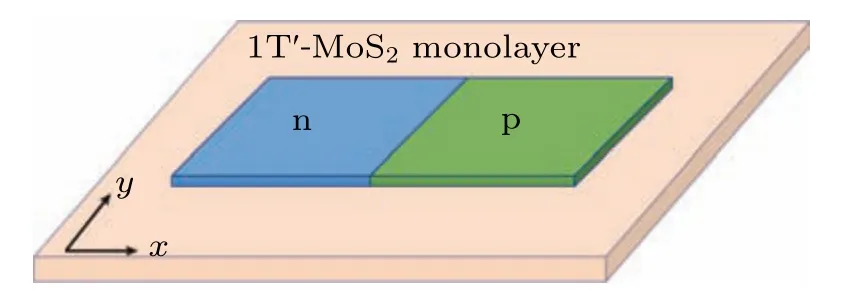
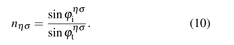
Fig.1. Schematic diagrams for 1T′-MoS2-based p–n junction.
2. Models and methods
The uniform Hamiltonian for 1T′-MoS2-based p–n junction shown in Fig.1 reads[6,22]
whereris the reflection coefficient andtis the transmission coefficient. The incident,reflected,and transmitted wavefunctions in each region are
3. Results and discussion
3.1. Anisotropic refraction
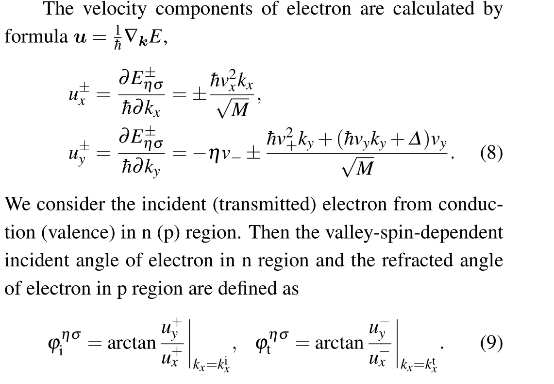
The valley-spin-dependent refractive index of electron is defined as
The valley-spin-dependent refractive index as a function of incident angle are given in Fig.2 in the different values ofα. The signs of refractive index for two valleys are opposite completely in Fig. 2 regardless of the value ofα. Although the spin-dependent refractive index in one valley can be tuned by the external electric field, the signs of refractive index for spin-up and spin-down in one valley are the same, as shown in Figs.2(b)–2(c). This unusual valley-spin-dependent refractive index brings exotic relations between incident angle and transmitted angle,as shown in Fig.3,in which the valley-spindependent transmitted angle as a function of incident angle is given in the different values ofα. In Fig.3(a)withα=0,the spin is degeneracy and the sign of transmitted angle is negative (positive) forΛ(-Λ) valley. In Figs. 3(b)–3(c) with the nonzeroα, the valley-spin-dependent transmitted angles are shown. Although the spin-dependent transmitted angles in one valley are different,their signs are the same in one valley.These results in Fig.3 are consistent with those in Fig.2 and will bring a potential application for valley splitting without any external fields.
Fig.2. Incident angle-dependent refractive index with ε =0.1 eV and V0=0.3 eV in the different values of α.
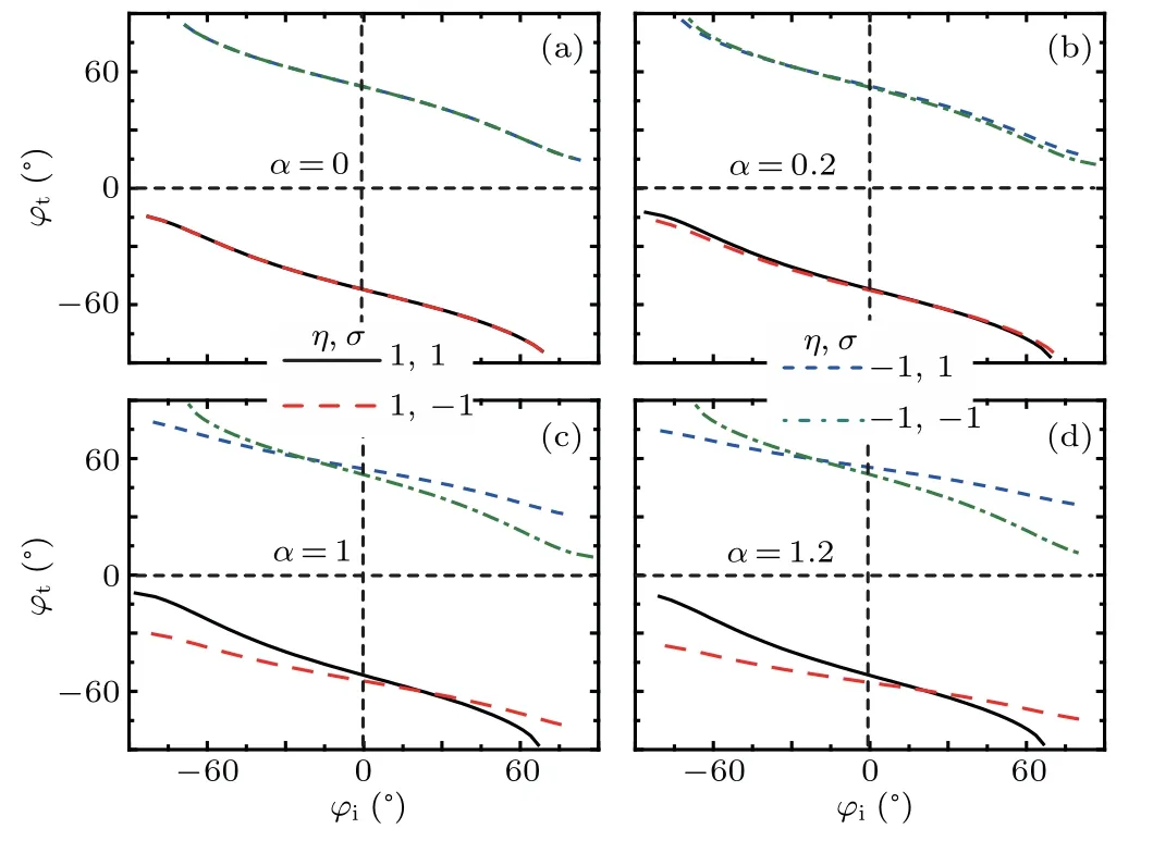
Fig.3. Incident angle-dependent transmitted angle with ε=0.1 eV and V0=0.3 eV in the different values of α.
Why does the valley splitting happen in a 1T′-MoS2-based p–n junction? Let us pay attention to Eq. (8). We assume physical parameterv-= 0, then the valley-spindependent incident angle of electron in n region and the refracted angle of electron in p region can be rewritten as
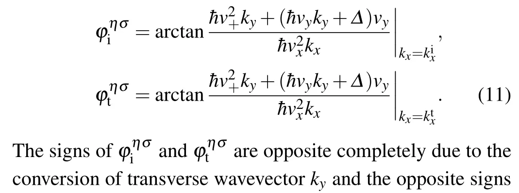
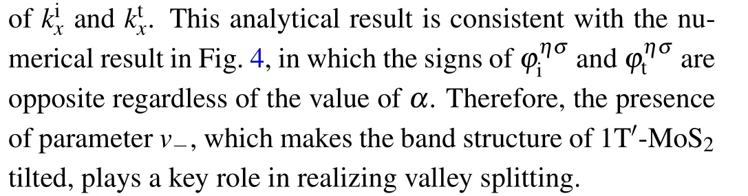
Fig. 4. Incident angle-dependent transmitted angle with ε =0.1 eV,v-=0,and V0=0.3 eV in the different values of α.
3.2. Valley-dependent anomalous Klein tunneling
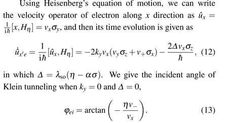
It is easy to obtainφei ≈-(+)36.5°forη=σ=1(-1) regardless of the value ofV0, which is the same as the numerical results in Figs. 5 and 6. Interestingly, the angle of Klein tunneling is dependent on the valley and spin simultaneously,which is different from the valley-spin-independent Klein tunneling and valley-dependent Klein tunneling.
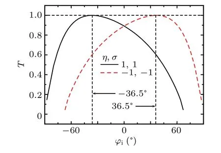
Fig.5. Incident angle-dependent transmission with ε =0.1 eV,α =1,and V0=0.3 eV.
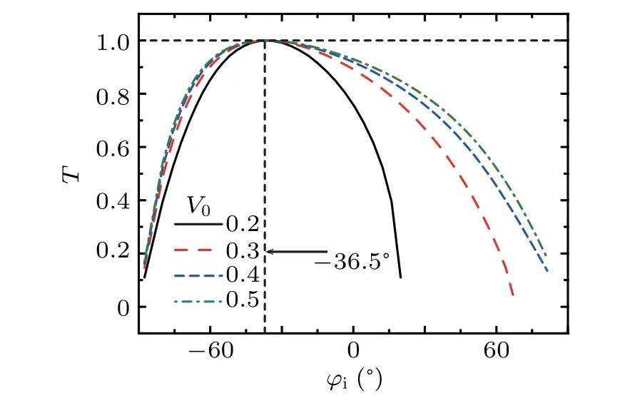
Fig.6. Incident angle-dependent transmission with ε =0.1 eV,η =1,σ =1,and α =1 for different values of V0.
4. Conclusion
We now give some discussions on experimental realization of our theoretical proposal. In experiment, the preparation of 1T′-MoS2 was reported in Ref. [55]. The 1T′-MoS2 based p–n junction can be realized by doping. The similar setup has been successfully realized for graphene.[52,56,57]A beam of electrons splits into two beams, which is the signature of valley splitting. The nonzero incident angle of electron for full transmission is the signature of anomalous Klein tunneling.
In conclusion, the transport properties of electron is investigated analytically in a 1T′-MoS2-based p–n junction.The anisotropic refraction consisting of positive and negative refractions is found, which leads to the valley splitting without any external fields. Interestingly, the nonzero incident angle of valley-spin-dependent anomalous Klein tunneling happens.These two peculiar properties come from the same fact that the tilted band structure makes the directions of wavevector and velocity different. Our work designs an special valley splitter without any external fields and provides an insight into the understanding of the Klein tunneling.
Acknowledgements
This work was supported by the National Natural Science Foundation of China (Grant Nos. 12104232, 11805103,and 11804167), the Natural Science Foundation of Jiangsu Province (Grant Nos. BK20190137 and BK20180739), the Innovation Research Project of Jiangsu Province (Grant No.CZ0070619002),and NJUPT-SF(Grant No.NY218128).

- Chinese Physics B的其它文章
- Solutions of novel soliton molecules and their interactions of(2+1)-dimensional potential Boiti–Leon–Manna–Pempinelli equation
- Charge density wave states in phase-engineered monolayer VTe2
- High-pressure study of topological semimetals XCd2Sb2(X =Eu and Yb)
- Direct visualization of structural defects in 2D semiconductors
- Switchable down-,up-and dual-chirped microwave waveform generation with improved time–bandwidth product based on polarization modulation and phase encoding
- Machine learning potential aided structure search for low-lying candidates of Au clusters