Modeling and numerical simulation of electrical and optical characteristics of a quantum dot light-emitting diode based on the hopping mobility model:Influence of quantum dot concentration
Pezhman Sheykholeslami-Nasab, Mahdi Davoudi-Darareh, and Mohammad Hassan Yousefi
Faculty of Science,Malek Ashtar University of Technology,Shahin-Shahr,Iran
Keywords: hybrid quantum dot light-emitting diode (QD-LED), concentration-dependent hopping mobility,effective transport model,Gaussian band structure
1. Introduction
The feasibility of electrical and optical simulation and modeling of quantum dot light-emitting diodes (QD-LEDs)is of great importance. These hybrid structures benefit from the variety of the organic transport layers as well as the high-performance optical properties of the semiconductor nanocrystals as the emitters.[1,2]Generally, the levels of the valence band (VB) edge and the conduction band (CB) edge of the QDs, respectively, are lower than the highest occupied molecular orbital(HOMO)and the lowest unoccupied molecular orbital(LUMO)of the commonly used organic transport layers; this leads to much more injection of electrons into the QDs.[3]The unbalanced injection of different charge carriers into the quantum dots (QDs) causes exciton quenching via non-radiative pathways like Auger recombination[4–6]and field-induced Onsager exciton dissociation.[7]Therefore, QD charging is one of the main challenges for the efficiency of QD-LEDs. Replacing the direct charge injection with exciton transfer mechanisms can be a solution to this problem. For this purpose, the QDs are incorporated into the host organic materials so that excitons generated on the host and their energies are then transferred to QDs via F¨orster resonant energy transfer (FRET).[2,8]The idea of using polymer: QD blends can overcome the poor structural stability,such as aggregation and grain boundaries observed in the QD-only layers,and can improve the device efficiency.[9–11]
Despite considerable experimental studies on hybrid QDLEDs, few theoretical modeling and numerical simulations have been performed. In previous work,[12]we introduced a model for simulating organic light-emitting diodes (OLED)with organic dopant in the emissive layer,in which the carrier mobility was described using the Poole–Frenkel model. This field-dependent mobility model is commonly used to calculate the mobility of the organic layers doped with organic emitters,in which the doping percent is generally lower than 1%. In QD-LEDs that typically have a high percentage of QDs embedded in the organic hosts, the mobility and, consequently,the current density characteristics, are strongly dependent on the concentration of QDs. Therefore, the Poole–Frenkel model, which is not explicitly dependent on concentration,cannot be a suitable model for describing the carrier mobility in QD-LEDs.[13]However, the hopping mobility[14–16]is constructed based on the Gaussian distribution of the densityof-states(DOS)[16]and the effective transport energy[14]models, and the dopant concentration is explicitly included in its formulation.The validity of these models in describing the energy distribution of organic layers doped with organic dopants and in calculating the carrier mobility of such films has been confirmed in other studies.[15,17]Some similarities between QDs and organic species in the localization and carrier transport gave us the idea that these models could be successful in describing the energy distribution and calculating the carrier mobility of polymer: QD blends.[13]
In this study, we utilize the hopping mobility model to calculate the carrier mobility in a polymer layer doped with different concentrations of QDs,which is used as a blend emissive layer of the hybrid QD-LEDs fabricated by Kanget al.[9]To verify the ability of the hopping mobility model to describe carrier mobility and charge transport in QD-LEDs,the simulation results will be compared with the electrical characteristics of the fabricated devices. Then, the exciton density profiles will be extracted based on the continuity equation for singlet and triplet excitons,and the corresponding luminance characteristics will be calculated and compared with the experimental data.
2. Theoretical models
2.1. Charge carrier transport model
The conventional framework used to obtain current density consists of drift-diffusion equations coupled with Poisson’s equation,[12,18]in which the drift-diffusion equations are continuity equations of charge carriers,and Poisson’s equation relates the electrostatic potential to the density of the charge carrier:[19]

whereμ0andE0are the zero-field mobility and characteristic electric field of the materials,respectively;Tis the device temperature;andEis the electric field. Due to the different work function of the electrodes and possibly the dipole layers at the electrode/organic interfaces, the relation between the applied voltage and the electric field should be written in the effective form[12]
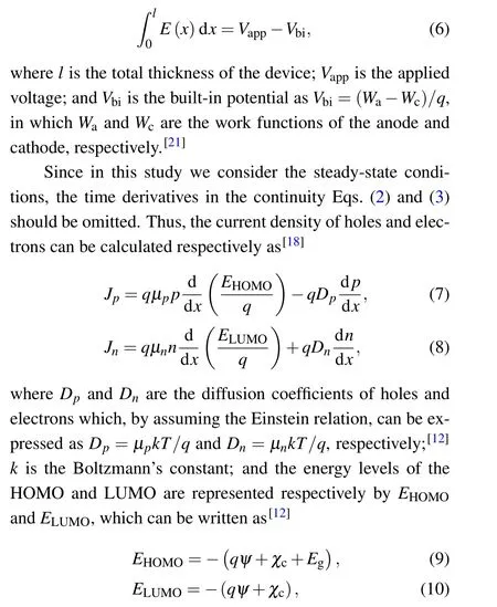
whereχcandEgare the electron affinity and the energy gap,respectively. We applied the Maxwell–Boltzmann statistics to calculate the density of holes and electrons in the organic charge-transporting layers as[12]


whereExis the energy component in thexdirection,his the Planck constant,andm*nis the electron effective mass. A similar relation can be written for the thermionic emission boundary conditions of holes.

We treated the contact of electrodes and the organic layers as a Schottky contact,[12]in which two components constitute the carrier current density: the thermionic emission and the tunneling.[24,25]Thus,the net current density of electrons can be expressed as

whereφn,b,0is the zero-field energy barrier for electrons. Similarly,the corresponding equations for holes can be written.
2.2. Gaussian distribution of DOS in doped organic films
It is well established that there are tail states in the Gaussian-like DOS of the organic layers,due to structural disorder,defects,and impurities.[27]Doping the organic host with the QD dopants broadens the DOS of the organic host significantly, and causes the deepest tail states to be filled and deactivated by charges introduced by the dopants. Arkhipovet al.[16,17,28]suggested that the broadening of DOS is due to the Coulomb interaction between ionized dopants and carriers. Their proposed model indicates that the energy disorder in doped organic materials is mainly due to van der Waals and dipole–dipole interactions within a system of molecules which are random in position and orientation.The ions of doped QDs in organic materials interact coulombically with localized carriers in intrinsic hopping sites and give rise to Coulomb potential fluctuations. Thus, doping of a disordered organic semiconductor further increases the energy disorder and will eventuate in broadening of the effective DOS distribution. On the other hand, doping increases the density of carriers that fill deep localized states and,consequently,raises the Fermi level and affects the energy gap of the host material. While the former effect strongly suppresses the hopping rate of carriers,the latter facilitates equilibrium conductivity. It has been shown both analytically and experimentally that,at high doping levels(more than 1%),the Coulomb-induced disorder tends to be saturated and the trap-filling effect dominates. Consequently,mobility steeply increases with the increasing concentration of dopants in the heavily doped organic materials.[17,28]
Generally, charge transport in organic semiconductors is modeled by carrier hopping within a Gaussian-like energy distribution, which is a relatively broad system of positionally random and energetically disordered localized states. When the QD dopants are incorporated into a random medium,their hopping sites are also affected by positional and energy disorder. In fact, doping of the organic layer with QDs varies the undoped DOS distribution of the pristine materials, and properly describing the mobility of carriers needs a strongly asymmetric distribution, rather than a Gaussian symmetric distribution.[28]Therefore, we can realistically describe the energy distribution of both organic host and QD dopants by a double-peak Gaussian function as[14–16]


wherep(n) is the total hole (electron) density in the valence(conduction)band;ph(nh)is the hole(electron)density of the host;pd(nd)is the hole(electron) density of the dopant; andfis the Fermi–Dirac function.
2.3. Effective transport energy and hopping mobility
Arkhipovet al.developed a variable-range hopping model based on the Miller–Abrahams equation for the hopping rate.[16]In this semi-analytical model for the hopping mobility in disordered organic doped materials, the hopping transport is a percolation problem, in which the average hopping rate and,concomitantly,the mobility are controlled by carrier jumps from deeper sites(in which most carriers are localized in equilibrium)to shallower sites(which play the role of transport states). The carrier hopping rate decreases strongly as the distance and energy between the starting and target sites increase. Thus, a carrier will most probably jump to a site corresponding to an optimized combination of the distance and energy difference;the temperature,carrier localization radius,and the shape of the DOS distribution determine the combinations. It has been shown both analytically[14]and by Monte–Carlo simulation[29]that if a DOS distribution is partially filled with carriers, there are the hopping sites, so-called effective transport levels of the energyEtr, such that a charge carrier will most likely jump from a currently occupied state to a hopping site[28](see Fig. 2). In other words, effective transport energy can be defined for a Gaussian DOS, at which charge carriers equilibrate over time after multiple hopping between the sites.[27]It is shown in Fig.2 that in a pristine organic material with a Gaussian DOS,the distribution of localized carriers has a maximum at the energy ofEm=-σ2/kTbelow the maximum of the intrinsic Gaussian distribution.[17]

The effective transport energy for holes and electrons(Etr,pandEtr,n)can be calculated respectively by[14–16]

where 1/γp(1/γn) is the carrier localization radius for holes(electrons). One can acquire the equilibrium hopping mobility by the procedure starting by using the Gaussian distribution of DOS described by Eqs. (20) and (21); then, by determining the quasi-Fermi energy of holes and electrons by Eqs.(22)and (23); next, by calculating the effective transport energy for holes and electrons by Eqs. (24) and (25); and finally, by computing the mobility of holes and electrons(μpandμn)respectively as[14–16]

2.4. Exciton continuity equations
The excitons are generated during the recombination of electrons and holes in the device; they can be annihilated via several processes. The continuity equations of the singlet and triplet exciton for the QD-LEDs have several generation/annihilation terms, which can be respectively written as[12,30]

where the notations are explained in the following:S(T)is the singlet(triplet)excitons density;kISCis the inter-system crossing constant;kRISCis the reverse inter-system crossing constant;krS=ηPL/τrS(krT=1/τrT) is the radiative decay rate for singlet (triplet) excitons, in whichηPLis the photoluminescence quantum efficiency (PLQE) andτrS(τrT) is the singlet(triplet)excitons’lifetime;knrS(knrT)is the non-radiative decay rate constant for singlet (triplet) excitons;kSS(kTT) is the bimolecular annihilation constant for the singlet–singlet(triplet–triplet) exciton annihilation process;DS=L2DS/τrS(DT=L2DT/τrT) is the singlet (triplet) exciton diffusion coefficient, in whichLDS(LDT)is the singlet(triplet)exciton diffusion length; andkFis the FRET rate, which is discussed separately in Subsection 2.5. We neglect the exciton quenching due to the diffusion of metallic atoms of the cathode into the adjacent organic layers, because of its small effect on the exciton density in the organic charge-transporting layers.
For the blend emissive layer, the contribution of QD dopants to the continuity equations of the singlet and triplet excitons should be considered as[12,18]

whereSd(Td) is the singlet (triplet) excitons density of dopants;krS,d=ηPL,d/τrS,d(krT,d=1/τrT,d)is the radiative decay rate for singlet (triplet) excitons of the dopants, in whichηPL,dis the PLQE andτrS,d(τrT,d) is the singlet (triplet) exciton lifetime of the dopants; andknrS,d(knrT,d) is the nonradiative decay rate constant for singlet (triplet) excitons of the dopants. The Langevin recombination rate at the host molecules in the emissive layer is determined using the carrier density in the host asRh=rphnhwhile,to determine the Langevin recombination rate at the dopants, the carrier density in the dopant should be considered asRd=rpdnd. Thus,there are two recombination rates at the emissive layer: one for the host molecules and another for the QD dopants. In this study,we neglect the dopant exciton diffusion and the dopant concentration quenching in the continuity equations of dopant excitons due to the presence of ligands and the relatively large distance between the QDs.
2.5. F¨orster resonant energy transfer
As mentioned in the introduction,we aim to activate and enhance the energy transfer to the QDs via FRET instead of the exciton forming on them. The rate of FRET between a donor and an acceptor located at a distancedcan be expressed as[31]
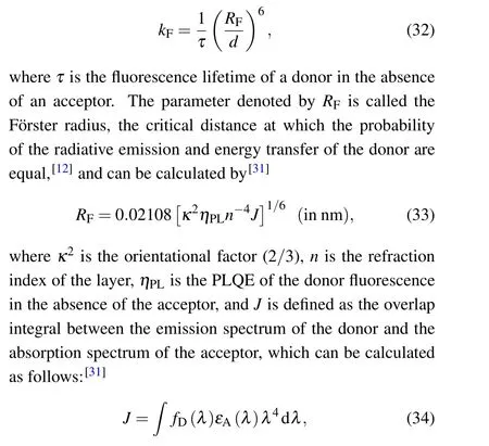
wherefDis the normalized fluorescence of the donor,εAis the molar extinction coefficient of the acceptor, andλis the wavelength.It is deduced from Eqs.(32)–(34)that the spectral overlap between the donor emission and the acceptor absorption spectra is a prerequisite for the FRET.
2.6. Luminescence model
When the singlet and triplet exciton profiles of the device(i.e.,the exciton density in a linear direction perpendicular to the center of the layers)are obtained using the exciton continuity equations,the luminescence characteristics of the device can be calculated. For this purpose, we use a model whose ability to accurately describe the luminance characteristics of the light-emitting devices has already been validated. The luminance of the QD-LED can be calculated in the photometric unit(candelas per square meter cd/m2)as[12,32]

wherehνspecifies the energy of emitted photons;nsubis the refractive index of the substrate;ηabscontains the efficiency loss due to absorption and light confinement in the layers;andV(λ) denotes the luminous efficiency function or eye sensitivity function.
3. Device structure
To evaluate the ability of this model to describe the electrical characteristics of QDLEDs, the measured data of a QD-LED (fabricated by Kanget al.[9]) were taken as a reference device, and calculations were performed for its structure with different concentrations. The fabricated device consists of an anode, a hole injection layer (HIL), a hole transport layer (HTL), a blend emissive layer (EML),an electron transport layer (ETL), an electron injection layer(EIL), and a cathode, respectively, as shown in Fig. 3(a).The device structure, from anode to cathode, is detailed as: indium tin oxide (ITO)/poly(3,4-ethylene dioxythiophene):poly(styrene sulphonate) (PEDOT:PSS)/poly(N,N′-bis(4-butylphenyl)-N,N′-bis(phenyl)benzidine) (poly-TPD)/poly(N-vinylcarbazole) (PVK):CdSe-QDs/tris(8-hydroxyquinolinato)aluminum (Alq3)/lithium fluoride(LiF)/aluminum (Al). A schematic energy diagram of the hybrid QD-LED is presented in Fig. 3(b), and the chemical structures of the organic materials used in the devices are presented in Fig.3(c).

To prepare the EMLs,the TOPO CdSe-QDs(Nanosquare Inc., Korea) with emission wavelengths of 530 nm (corresponding to the 2.6 nm CdSe-QDs[33]) as monochromatic emitters and PVK (Sigma-Aldrich Co. LLC) as the host matrix were used by the spin-coating method.[9]PVK has shown great capability to incorporate QDs and,over the last decade,many researchers have focused on designing hybrid QD-LEDs based on the PVK:QD emissive layer.[9,34–40]The attained concentration ratios of the EMLs, in the form of PVK:CdSe-QDs,were 1:0.5,1:1,and 1:2,which are denoted as devices A,B,and C,respectively. The optical characteristics of the materials used in the EML are represented in Fig.4, which shows the PL spectra of the PVK and the absorption of the CdSe nanocrystals. There is a clear spectral overlap between the emission of PVK and the absorption of CdSe QDs,suggesting the possibility of efficient FRET from PVK molecules to CdSe nanocrystals.By calculating the overlap integral(Eq.(34))using the measured spectra of the PVK emission and CdSe absorption and then inserting it into Eq.(33), the F¨orster radius was defined asRF≈9.4 nm.

4. Numerical solution methods
Due to the simple device geometry(Fig.3(a)), there is a lateral invariance which causes the state variables to have constant values in a certain monolayer parallel to the electrodes.Thus, it is principally sufficient to use a one-dimensional device modeled along an axis perpendicular to the center of the layers, starting from the anode and ending at the cathode.[43]The Scharfetter–Gummel method[44]is used to discretize the space to solve the coupled, non-linear, and partial differential equations described in the theoretical models (Eqs. (1)–(3); (7) and (8); and (28)–(31)). This discretization method converts the continuous nature of the problem to a discretized non-linear algebraic system that has roughly the same behavior. The discretized system was solved using Newton’s iterative method[45]so that an estimated solution becomes more accurate consecutively,and the procedure was continued until the convergence criteria were satisfied.[12]The applied voltage to each electrode starts at zero bias and increases stepwise. At each bias point,the charge carrier density profile,the extent of the Langevin recombination rate,and the exciton density profile are calculated;then the current density and luminance are obtained based on them.
5. Simulation results and discussion
The essential parameters for simulating the carrier transport are the energy levels(electron affinity and energy gap of the organic materials, and work functions of the electrodes),permittivity of the materials,DOS of the carriers,and the carrier mobility parameters.The energy levels and permittivity of the organic layers are shown in Table 1,which are taken from experimentally measured data.[46–52]The work function of the ITO and LiF/Al are 4.7 eV and 2.8 eV, respectively.[53,54]In this study, the DOS of the carriers in the HOMO and LUMO,NHOMOandNLUMO, are taken as 1×1020cm-3for all materials.[18]
The carrier mobility in the organic layers is calculated by the Poole–Frenkel model using the parameters listed in Table 2, which are taken from experimental measurements.[18,55,56]This model cannot describe the dependence of carrier mobility in the EML on the concentration of QDs. For the EML, we used a proposed model based on the Gaussian distribution of energy states[16]and the effective transport energy,[14]called the hopping mobility model.

Electron affinity Energy gap Permittivity χc (eV) Eg (eV) εr PEDOT:PSS 2.7 2.4 2.2 Poly-TPD 2.3 2.9 3.5 PVK 1.9 3.5 3.0 Alq3 2.4 3.1 3.3

μ0n E0n μ0p E0p(cm2/V·s) (V/cm) (cm2/V·s) (V/cm)PEDOT:PSS 1.00×10⁻⁹ 1.08×10⁴ 2.40×10⁻⁶ 2.27×10⁴ Poly-TPD 1.00×10⁻⁹ 1.08×10⁴ 1.70×10⁻³ 2.51×10⁴ Alq3 1.51×10⁻⁷ 1.01×10⁴ 9.16×10⁻¹⁰ 1.09×10⁴
Density,width,and the center of the Gaussian peak of the host and dopants are necessary to form the Gaussian energy distribution in the EML and can greatly affect the resulting hopping mobility. Based on the results of research on the size and ligand effects on the DOS of CdSe nanocrystals,[57–59]we deduce that the QDs used in this study have a Gaussianlike peak in the CB with an energy ofECB=2.2 eV and a Gaussian-like peak in the VB with an energy ofEVB=5.6 eV.On the other hand, the PVK HOMO and LUMO energy levels are measured[60]atEHOMO=5.5 eV andELUMO=2.2 eV.Therefore,the QD’s CB peak is aligned with the PVK HOMO peak, and the center of the QD’s VB peak is 0.1 eV outside the PVK gap. After estimating the location of the center of the Gaussian peaks for the host and dopants, we proceed to determine its width and density. Typical values for effective width (σ) and density (N) of the Gaussian peaks to describe energy distribution of the doped polymers have been reported in the ranges of 0.03 eV–0.15 eV and 1019cm-3–1022cm-3, respectively,[16,17,28]considering thatσDopants>σHost andNHost>NDopants.
We optimized the density and width of Gaussian peaks of the host and dopants to obtain an appropriate description of DOS that could fit the current–voltage results to the experimental data of the reference device. In fact, to evaluate the capability of the proposed model to describe the mobility of organic layers doped with QDs,we used the phenomenological fitting of the simulation results. At the beginning we followed the parameters of the host material,using experimental results for the undoped device.[9]A PVK film has a density of 1.2 g/cm3[61,62]and a molecular weight of 193.24 g/mol,[63,64]so its molecular density is about 3.7×1021cm-3. With this initial guess for the density of host states and by comparison with current–voltage characteristics of the undoped device,the optimal values of the density and width of the Gaussian peak of PVK were obtained as 4.6×1021cm-3and 0.036 eV, respectively.
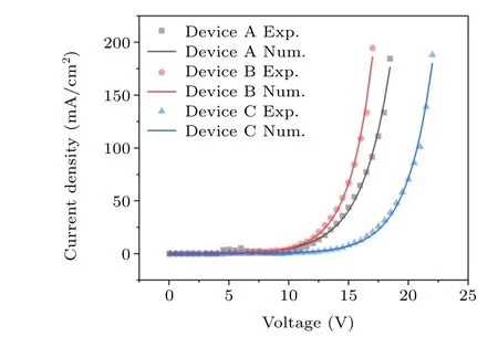
Then, we sought the parameters needed to correctly describe the Gaussian peak of QD dopants in devices A–C. It should be noted that, for the preparation of EML in each device, a certain weight ratio of host and dopant was used to prepare a solution in the form of PVK:CdSe-QD and then this solution was spin-coated. Therefore,using the density of 2.6 nm CdSe-QD(about 2.4 g/cm3)and the PVK density,one can convert the weight ratio of EMLs to the corresponding volume ratio. The volume percent of CdSe-QDs in the EML of devices A–C can be calculated as 20%, 33.3%, and 50%,respectively, which we call the volume percent constant and denote ascVP. We applied the effect of doping on the DOS of EML in Eqs. (20) and (21) by multiplying the Gaussian peak densities of the dopant and host incVPand(1-cVP),respectively. Given thatcVP=20%and by fitting the simulated results of the current–voltage characteristics to the experimental data of the reference device A, we obtained the density and width of the Gaussian peak of QD dopants as 0.075 eV and 2.9×1022cm-3, respectively. By fixing the Gaussian peak width of QD dopants and varying its density by a volume percent constant, we fitted the current–voltage characteristics of devices B and C to their corresponding experimental data;therefore, the volume percent constants for devices B and C were obtained as 36.6%and 53.8%,respectively. The parameters required to describe the double-peak Gaussian distribution of the EML of devices A–C are listed in Table 3.

NHOMO,NLUMOa (cm-3) σHOMO,σLUMO (eV) cVP NVB,NCBb (cm-3) σVB,σCB (eV) ΔEV (eV) ΔEC (eV)Device A 3.7×10²¹ 0.036 20% 5.8×10²¹ 0.075 -0.1 0 Device B 2.9×10²¹ 0.036 36.6% 10.6×10²¹ 0.075 -0.1 0 Device C 2.1×10²¹ 0.036 53.8% 15.6×10²¹ 0.075 -0.1 0
The distribution of energy states in the EML of devices A–C was constructed by using the parameters listed in Table 3 and Eqs. (20) and (21), and the corresponding double-peak Gaussian graphs are presented in Fig.5. Each of the conduction peaks in this figure is the result of overlapping two peaks:one to describe the DOS of the PVK,and the other to describe the DOS of the CdSe-QDs. Meanwhile, the valence peaks of the host and dopants are separated by 0.1 eV.Then,we calculated the Fermi energy, the effective transport energy and the hopping mobility of the EML by utilizing Eqs. (22)–(27). In this study,the carrier localization radius(1/γ)in Eqs.(24)and(25),and the attempt-to-jump frequency(ϑ0)in Eqs.(26)and(27),are taken as 0.2 nm and 8×10¹²s-1,respectively.[16,28]
The measured current density characteristics of the fabricated devices A–C are compared to the numerical results in Fig.6. It can be seen from the figure that the turn-on voltage(Vto) of the hybrid QD-LEDs decreases when the CdSe-QD concentration increases from 0.5 wt%in device A to 1 wt%in device B;then,when the concentration increases to 2 wt%in device C, it demonstrates counterproductive behavior andVtotends to move strongly towards higher voltages.

To investigate how carrier mobility has influenced the current density of devices A–C, the mobility of electrons and holes, calculated by Eqs. (26) and (27), is shown in Fig. 7.It can be seen from the graph that the electron mobility increases when raising the concentration of QDs, although its behavior is not linear. On the other hand,as the concentration of QDs rises from device A to device B,the hole mobility also increases; but when further raising the concentration of QDs,the hole mobility decreases sharply. Therefore, the constructive and non-constructive effect of the concentration of QDs on the current intensity characteristics of the devices is mostly attributed to changes in the hole mobility and slightly due to the electron mobility.

The effect of QD concentration on the hole mobility and current density can be explained by the distribution of energy states in the EML of hybrid QD-LEDs. In fact, enhancement of the QD concentration broadens the DOS of the EML and progressively creates many hopping sites inside the gap. Increasing the QD concentration also enhances the density of charge carriers,while the energy distribution of trapped carriers becomes shallower. This situation results in a higher average jump rate and sharply increasing mobility.[17,28]According to Fig. 5, the Gaussian energy distribution of QDs in devices A and B causes the PVK Gaussian peak to be higher and wider. Therefore, increasing the concentration of QDs from device A to device B improves the hole mobility. In device C,we face a different situation;although,when increasing the QD concentration in the EML as PVK:CdSe-QD from 1:1 in device B to 1:2 in device C,there is a growth in the peak of the host material, but the excessive growth of the QD peak shifts the effective transfer energy to out of the gap. Therefore, the energy distribution of trapped carriers becomes deeper,which leads to steeply decreasing hole mobility. From an experimental point of view, the drastic regression in the electrical efficiency at a higher doping concentration can be attributed to the aggregation of QDs and the formation of grain boundaries. It is worth noting that we did not find a way to methodically vary the parameters of other models to describe the dependence of carrier mobility on the concentration of dopants in the blend layer, so we could not compare the results of our proposed model with the other models.
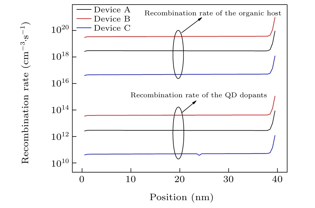
In the following, the effect of QD concentration on the luminescence efficiency of QD-LEDs is investigated by calculating the luminance characteristics of the devices. For this purpose, a model based on the exciton density in the device was used,which was successfully validated for OLEDs in our previous study.[12]Of course, here we also included the contribution of triplet excitons in the model due to the presence of QDs. The formation of excitons in the device takes place during the recombination process. The recombination rate in the EML of devices A–C was calculated based on the Langevin recombination model,and the resultant profiles atVapp=16.5 V are shown in Fig.8. According to the figure,we find that the rate of exciton formation in PVK molecules is much higher than QDs,which indicates a slight direct charge injection into the QDs. Then,using Eqs.(28)–(31),the exciton densities in the organic host and QD dopants were calculated;the resultant profiles atVapp=16.5 V are presented in Fig.9. It is clear in this figure that the exciton density in the host is several times lower than in the dopants. Therefore, from the results of the recombination rate and the exciton density, we can conclude that the excitons mainly form at the host molecules and are well transferred to the QDs during the FRET process. Both the recombination rate at the host and the exciton density in the QDs are higher in device B than in the other two devices,which ensures higher luminescence efficiency.

ηPL τrS (ns) LDS (cm) kSS (cm3·s-1) τrT (ns) LDT (cm) kTT (cm3·s-1)PVK 0.42 8.3 8.9×10⁻⁷ 2.0×10⁻¹⁰ 800 6.3×10⁻⁶ 1.6×10⁻¹⁰ CdSe-QDs 0.35 9.0 – 3.0×10⁻⁸ 9.2 – 4.2×10⁻¹¹


Based on the exciton density profiles and from Eq. (35),the luminance characteristics of devices A–C were calculated;the results are compared to the experimental data of the reference devices in Fig.10. An accurate description of the carrier mobility and subsequently obtaining the proper density of the carrier and exciton in the device made it easy to fit the luminance characteristics of the devices to the experimental data.The required parameters for calculating the exciton density in the PVK host and CdSe-QD dopants are listed in Table 4. It has been confirmed that in the PVK,the contribution of intersystem crossing and reverse intersystem crossing mechanisms to the relaxation of singlet excitons is negligible, and the efficient mechanism is FRET.[65]In the simulation of similar devices,the non-radiative decay rate constants for singlet and triplet excitons have also been set to zero due to their negligible effect on exciton density.[30]So, we ignored the rate of these mechanisms when calculating the luminance of devices.It can be seen from Fig. 10 that, similar to the current density characteristics, device B has much higher luminescence efficiency than the other two devices at any applied voltage.
Despite the advantages of QD-LEDs, such as easy tuning of the emission color by adjusting the particle size, saturated color purity, and a low-cost solution-processed fabrication method, their luminance characteristics are generally lower than those of OLEDs. Although,with the incorporation of CdSe QDs within the PVK matrix in the reference devices and by optimizing the QD concentration, one of the major causes of the low efficiency of QD-LEDs(i.e.,the aggregation and grain boundary of the QDs)has been improved;it can be said from Fig. 10 that the luminance of devices A–C are still lower than common OLEDs.In fact,the external quantum efficiency(EQE)of QD-LEDs is limited by the PLQE of the QDs in a thin film. By employing material with a higher PLQE,the EQE should proportionally increase.[7]Surface modification methods,such as polymer encapsulation,surface grafting,and ligand exchange,can improve the PLQE of the QDs up to 30%due to better packing of the QD surface and passivation of the PL quenching defects.[66,67]Another solution for the poor PLQE of QDs is the shelling of inorganic atomic layers with a wider bandgap on the surface of core QDs, which enhances the PLQE by effectively reducing the nonradioactive recombination.[68]Although the PLQE of core-only QDs has been reported to be lower than 50%, the best reported values of PLQE are around 80% for inorganic-shelled QDs, which is competitive with organic species. Another important factor that has an influence on the device efficiency is the arrangement of energy levels, which controls the density of charge carrier in the layers. The energy diagram of the QD-LED should be designed to maximize the amount and alignment of different charge carriers in the emissive layer, which improves the exciton formation rate and,consequently,the luminescence efficiency of the device.[69]
6. Conclusion
A comprehensive numerical framework for the electrical and optical simulation of hybrid QD-LEDs, with a blend emissive layer consisting of an organic matrix and different concentrations of QD dopants, was investigated. The ability of the proposed model to describe the current density and luminance characteristics of QD-LEDs was evaluated by comparing and fitting the simulation results to the measured data of the reference device as ITO/PEDOT:PSS/poly-TPD/PVK:CdSe-QDs/Alq3/LiF/Al with different concentrations of QDs in the emissive layer. To describe the electrical characteristics of the devices, a hopping mobility model was constructed based on the Gaussian distribution of DOS and the effective transport energy models. The results show that the proposed model based on hopping mobility can correctly describe the concentration-dependent electrical behavior of QDLEDs. Then,based on the continuity equation for singlet and triplet excitons,the exciton density profiles of QD-LEDs were extracted and the corresponding luminance characteristics of the devices were calculated. The results of the luminescence model are in good agreement with the experimental data of the reference devices.It is concluded that the proposed framework can be successful in describing the transport of charge carriers and excitons in QD-LEDs. So, we adapted the hopping mobility model to calculate the carrier mobility in the polymeric emissive layer blended with QDs, and successfully evaluated the model efficiency by comparing the numerical results with the experimental data. The proposed model could be a way to fill the research gap in the field of simulation of hybrid QDLEDs that have a blend emissive layer.
- Chinese Physics B的其它文章
- Ergodic stationary distribution of a stochastic rumor propagation model with general incidence function
- Most probable transition paths in eutrophicated lake ecosystem under Gaussian white noise and periodic force
- Local sum uncertainty relations for angular momentum operators of bipartite permutation symmetric systems
- Quantum algorithm for neighborhood preserving embedding
- Vortex chains induced by anisotropic spin–orbit coupling and magnetic field in spin-2 Bose–Einstein condensates
- Short-wave infrared continuous-variable quantum key distribution over satellite-to-submarine channels

