Recent Developments of Transmissive Reconfigurable Intelligent Surfaces:A Review
TANG Junwen,XU Shenheng,YANG Fan,LI Maokun
(Department of Electronic Engineering,Tsinghua University,Beijing 100084,China)
Abstract:Reconfigurable intelligent surface(RIS)is considered as one of the key technologies for the next-generation mobile communication systems.The transmissive RIS is able to achieve dynamic beamforming capability while transmitting an in-band RF signal through its aper‑ture,and has promising prospects in various practical application scenarios.This paper reviews some of the latest developments of the trans‑missive RIS.The approaches for transmissive RIS designs are classified and described briefly.Numerous designs with different phase resolu‑tions,such as 1-bit,2-bit or continuous 360° phase shifts,are presented,with detailed discussions on their operating mechanisms and trans‑mission performances.The design solutions for various transmissive RIS elements are summarized and compared.
Keywords:antenna;mobile communications;phase shifter;RIS;transmitarray
1 Introduction
As one of the key technologies for the next-generation mobile communication systems,the reconfigurable in‑telligent surface (RIS)[1-3]has attracted great atten‑tions recently.On the contrary to the commonly used reflection mode,the transmissive RIS is able to achieve dy‑namic beamforming capability while transmitting an in-band RF signal through its aperture.This distinctive feature allows much improved direct indoor coverage by the outdoor cellular signals.It can also be employed as a reconfigurable radome for 5G base station antennas or terminal antennas.The largescale RIS array can effectively boost the coverage of the medium-sized 5G massive multiple-input multiple-output(MIMO) antennas,and the analog-digital hybrid structure can keep the overall cost and power consumption low.
Solid-state electronic devices are commonly integrated in each constituent RIS element to achieve phase reconfigurabil‑ity.Continuous phase shifts can be realized using analog-type devices like varactor diodes[4-13].The phase shift range usually exceeds 360°so that the phase errors are negligible.However,the transmission insertion loss of the RIS element is relatively high and for instance,can be up to 5.7 dB[7],considerably re‑ducing the aperture efficiency of the RIS.Switch-type devices,such as p-i-n diodes and radio frequency (RF) microelectro‑mechanical system (MEMS) switches,are widely used to pro‑duce discrete phase shifts[14-31],especially at millimeter wave frequencies.Most designs focus on 1-bit phase reconfigurabil‑ity because the complexity in design and fabrication is more manageable[14-27].The phase quantization errors associated with discrete phase shifts inevitably introduce performance degradation[32-34].It is observed that the 1-bit designs suffer from 3-4 dB loss attributed to the coarse phase resolution,re‑sulting in low aperture efficiencies.The sidelobe levels are usu‑ally much higher,sometimes even causing unwanted grating lobes.The 2-bit design is considered a well-balanced choice between the design complexity and the element performance.The phase quantization loss can be greatly reduced to less than 1 dB,and the sidelobe envelop is much improved as well[28-31].
Most transmissive RIS designs are based on the receivertransmitter (Rx-Tx) structure[4-9,14-22,25-31],and microstrip patch antennas[4-9,14-18,20-21,25-26,30],slot antennas[19,28-29],viv‑aldi antennas[22]and dipole antennas[27,31]are employed as re‑ceivers or transmitters.There are a handful of designs using the stacked frequency selective surface (FSS) struc‑tures[10-13,23-24].Each FSS layer provides a finite-degree phase shift,and a wide phase shift range is achieved by stacking multiple FSS layers.The structure is relatively more compli‑cated and more solid-state electronic devices are needed in each unit cell.
This paper provides a review of some recent transmissive RIS studies and is organized as follows.The configuration classification of the transmissive RIS is introduced in Section 2.Various transmissive RIS designs with different phase reso‑lutions or polarizations are described in Section 3.Finally,conclusions are given in Section 4.
2 Design Approaches
There are two widely used design approaches for the trans‑missive RIS,which are the receiver-transmitter (Rx-Tx) struc‑ture and the stacked FSS structure.Generally,a typical Rx-Tx structure consists of three components:the receiving (Rx)cell,the transmitting (Tx) cell,and the power transmission structure.A ground plane separates the Rx from the Tx,so that they can operate independently,avoiding the mutual in‑terference with each other.The power transmission structure between them is usually realized by a metallic via[7-9,14-18,20-21,25-27,30]or a slot-coupling structure[4-6].When the RIS is illuminated by an incident wave,the Rx on one side of the RIS first receives the wave and converts it into a guided wave.This wave is then conveyed through the power transmission structure to the Tx deployed on the other side of the RIS,and re-radiated to the free space.The phase shift can be realized on either the Rx,the Tx,or the power transmis‑sion structure.
The stacked FSS structure type is inspired by the classic FSS designs.It consists of multiple FSS layers of metallic and dielectric substrates.A phase shift with finite degrees is ob‑tained when a wave propagates through each FSS layer,and by cascading multiple layers,a larger phase shift can usually be realized.The separation between layers is also a crucial pa‑rameter.The overall thickness is relatively large.Unlike the Rx-Tx type,there is no ground plane in the stacked FSS struc‑ture type(Fig.1).
3 Representative Transmissive RIS Designs
3.1 Single-Polarized 1-Bit Designs
A 1-bit transmissive RIS element can realize two phase states with a phase difference of 180°.Generally,there are two operating mechanisms in the element designs,which are the current reversal method and the variable resonance method.The current reversal method based on the Rx-Tx structure is most popular for 1-bit designs in literature.The p-i-n diode is usually chosen as the controlling device due to its small volume and stable performance especially at high fre‑quencies.The p-i-n diode can work at“ON”or“OFF”states by supplying a different DC biasing signal.In practice,two p-i-n diodes are usually embedded in parallel and in op‑posite directions in each element,and a single positive or negative biasing signal can switch them between the“ONOFF”and“OFF-ON”states.Hence,the excitation current on the radiating element flows in opposite directions,and the radiated field is reversed,resulting in a stable phase shift of 180°.The stacked FSS type structure is usually based on the variable resonance method.The resonant characteristic of the element structure is manipulated by switching the integrated p-i-n diode“ON”or“OFF”,and consequently,a phase differ‑ence in its radiated field is caused.It is noted that the phase difference varies with frequency,and its bandwidth is usually narrower than that using the current reversal method.
Single polarized 1-bit RIS has been widely investigated.A representative linearly polarized design with an O-slot patch and two p-i-n diodes based on the Rx-Tx structure and the current reversal mechanism is proposed in Ref]14],as shown in Fig.2(a).The element evolves from the U-slot microstrip patch antenna.It is modified into an O-slot so that two p-i-n diodes placed across it and biased in opposite states can effec‑tively form a U-slot patch with reversible direction,thereby achieving a phase difference of 180° due the current reversal mechanism.A metallic via connecting the Rx and the Tx is used to transmit the signal from the incident side to the reradiating side.The measured transmission insertion loss is 1.7/1.9 dB for two states and the 3-dB transmission bandwidth is 14.7%.Moreover,the DC biasing circuit is elaborately de‑signed.The positive end of one p-i-n diode and the negative end of the other are connected together through two symmetri‑cal metallic vias.Only a single DC biasing signal is required to control them working at opposite states.The biasing lines are arranged close to the ground,thus minimizing its interfer‑ence on the RF performance.It is also worth mentioning that by truncating the corners of the U-slot patch or modifying the U-slot patch,the 1-bit linearly polarized element can be readily developed into a single linear-circular polarization conversion[16,18]or polarization switching designs[17].The sketch of the element in Ref]16] is shown in Fig.2(b).A minimum transmission insertion loss of 1.59/1.70 dB at Ka band with a 3-dB bandwidth of more than 12% is validated in measurement.
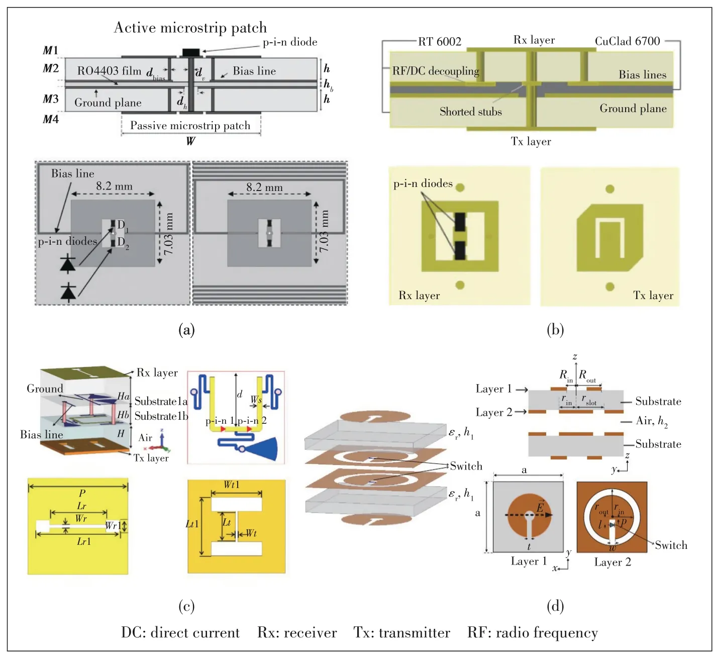
▲Figure 2.Schematics of single-polarized 1-bit transmissive reconfigurable intelligent surface(RIS) elements:(a) linear polarization in Ref]14];(b) linear-circular polarization conversion in Ref]16];(c)slot coupling structure in Ref]19];(d)variable resonance design in Ref]23]
The 1-bit element presented in Ref]19] exploits two slot antennas as Rx and Tx.As Fig.2(c)shows,two H-shaped slots are placed orthogonally to receive and re-radiate electromag‑netic waves,with high polarization isolation due to the polar‑ization orthogonality.Two p-i-n diodes are integrated in the Ushaped transmission line to control the excitation current di‑rection.By switching them working at“ON-OFF”or“OFFON”state,the electric field coupled to the Tx H-slot is re‑versed,resulting in a 180° phase shift.The operating fre‑quency of the element is 12.5 GHz,and the simulated trans‑mission insertion loss is 0.86/0.76 dB.
A 1-bit element design based on the variable resonance method is proposed in Ref]23],and the element configura‑tion is shown in Fig.2(d).It is com‑posed of four metallic layers and two layers of dielectric substrates.The up‑per and lower C-shaped patches are uti‑lized for the transmission of the electro‑magnetic waves,with two ring slots loaded by a rectangular gap used as the phase shifter.Two p-i-n diodes are po‑sitioned across the two rectangular gaps and work at“ON-ON”or“OFFOFF”state.They change the widths of the gaps,and consequently,the equiva‑lent resonance length varies,thus shift‑ing the transmission phase of the ele‑ment.The measurement shows that the element transmission insertion losses for the two phase states at 11.5 GHz are 0.6 dB and 2.9 dB,respectively.Note that the transmission insertion loss increases due to the detuning of the resonant characteristic of the ele‑ment structure when the 180° phase shift is realized.
3.2 Dual-Polarized 1-Bit Designs
The dual-polarized transmissive RIS designs mostly focus on 1-bit phase resolution.In general,there are two so‑lutions.One is to excite two orthogonal radiating modes of the same radiator[25],and the other is to arrange two sets of single-polarized 1-bit RIS elements or‑thogonally to achieve the dual-polarized function[24,26-27].Note that there are some designs with the polarization ma‑nipulation capability[7,17-18];however,they are unable to op‑erate in two polarization directions simultaneously and hence excluded in this section.
The dual-linear polarized 1-bit element proposed in Ref]25]exploits a five-layer-stacked configuration.The element con‑figuration is illustrated in Fig.3(a).For the realization of the single-linear polarized 1-bit phase controlling,it relies on the U-shaped feeding line integrated with two p-i-n diodes.By al‑ternatively switching the working states,the radiated fields in opposite direction are excited on the top metallic square ring,and a 180° phase difference can be generated.A dual-linear polarized design can be achieved by employing two orthogo‑nally placed U-shaped feeding lines to excite the same metallic square ring.The measured results show that this element can achieve a transmission insertion loss of 1.7/1.9 dB at 5.9 GHz,with an operating bandwidth of 2.8%.
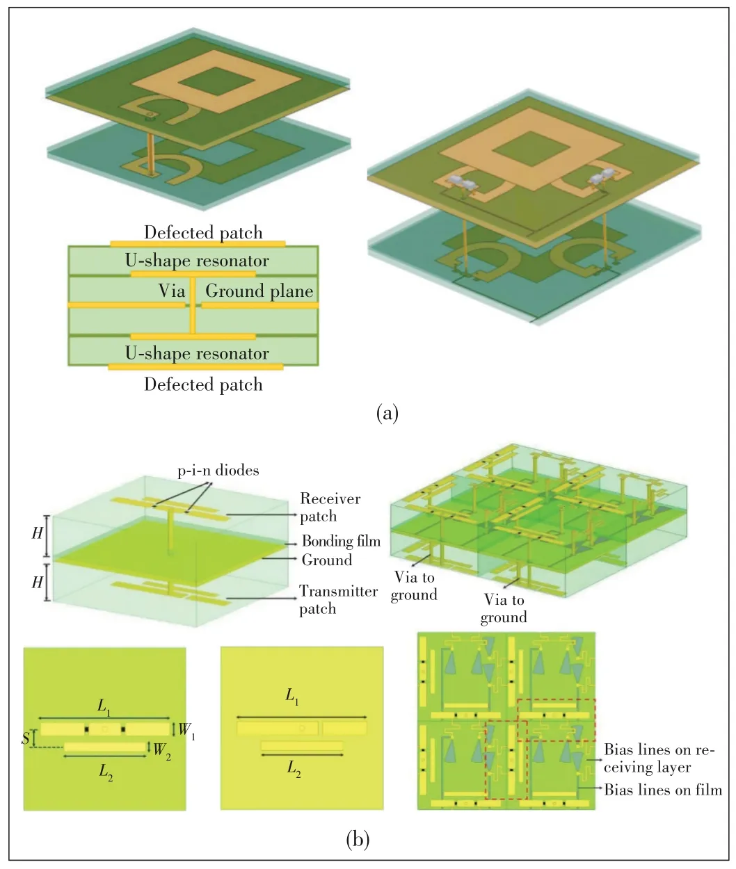
▲Figure 3.Schematics of the dual-linear polarized 1-bit transmissive re⁃configurable intelligent surface (RIS) element designs:(a) two orthogo⁃nal radiating modes of the same radiator in Ref]25];(b)two sets of viafed dipoles with parasitic dipoles in Ref]27]
Ref]27]presents a dual-linear polarized 1-bit RIS element based on a via-fed dipole with a parasitic dipole.Fig.3(b)de‑scribes the fundamental single-polarized 1-bit RIS element.The element employs the Rx-Tx structure,both based on di‑pole configurations.Two p-i-n diodes are placed on the arms of the receiver dipole,and a parasitic dipole is added near the dipole to reduce the loss.The mechanism can be ex‑plained as the current is mostly coupled to the parasitic di‑pole,reducing the loss that is caused by the current flowing through the p-i-n diodes.Therefore,the simulated element transmission insertion loss is only 0.8 dB at 12.25 GHz.The design of the dual-linear polarized element can be accom‑plished by arranging two sets of single-linear polarized ele‑ments orthogonally.
3.3 2-Bit Designs
Although considerable developments of the 1-bit transmis‑sive RIS designs have been accomplished,they still suffer from suboptimal radiation behavior caused by the large phase quantization error.In order to increase the phase accuracy so as to improve the radiation performance,the 2-bit design is in‑vestigated.
Another 2-bit RIS element at Ka band is proposed in Refs]28-29].As illustrated in Fig.4(a),the Rx and Tx slots are fed with striplines,and five RF MEMS switches are loaded on the striplines to switch the four operating modes alternatively.The measured element transmission insertion loss,however,reaches up to 4.2-9.2 dB due to the challenging fabrication process.A Ka-band linearly polarized 2-bit RIS element is presented in Ref]30].The configuration of the element is de‑picted in Fig.4(b).It is composed of six metallic layers and three dielectric substrates,with four integrated p-i-n diodes.The 180°phase shift is realized by alternating the two p-i-n di‑odes loaded on the receiving O-slot patch.Two more p-i-n di‑odes are loaded on the transmitting patch,which contains a de‑lay line to achieve the additional 0°/90° phase switching.Thus,the 2-bit phase tuning capability can be obtained.The measured element insertion loss is 1.5-2.3 dB for the four phase states at 29 GHz,with the measured 3-dB transmission bandwidth of 10.1%-12.1%.
3.4 Designs with Continuous Phase Shift
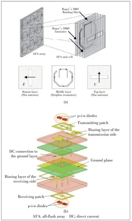
▲Figure 4.Schematics of the 2-bit transmissive reconfigurable intelli⁃gent surface (RIS) element designs:(a) dual polarization with five radio frequency (RF) microelectromechanical system (MEMS) switches in Refs]28-29];(b)O-slot patches loaded with four p-i-n diodes in Ref]30]
To achieve a continuous 360° phase shift,varactor diodes are widely utilized in most transmissive RIS element designs since the capacitance of the varactor diodes can be changed by applying a DC biasing voltage.One phase tuning approach is based on the microstrip phase shifter[4-5,7-9].By employing the Rx-Tx structure,the varactor diodes are placed on the phase shifter to control the transmission phase,ensuring the stability of the transmission insertion loss in the operating fre‑quency band when the DC biasing voltage changes.Thus,most wideband RIS designs explore this approach to tune phase shift.The other approach is to change the resonant char‑acteristic of the element structure[6,10-13],and it is widely used in the stacked FSS structures.
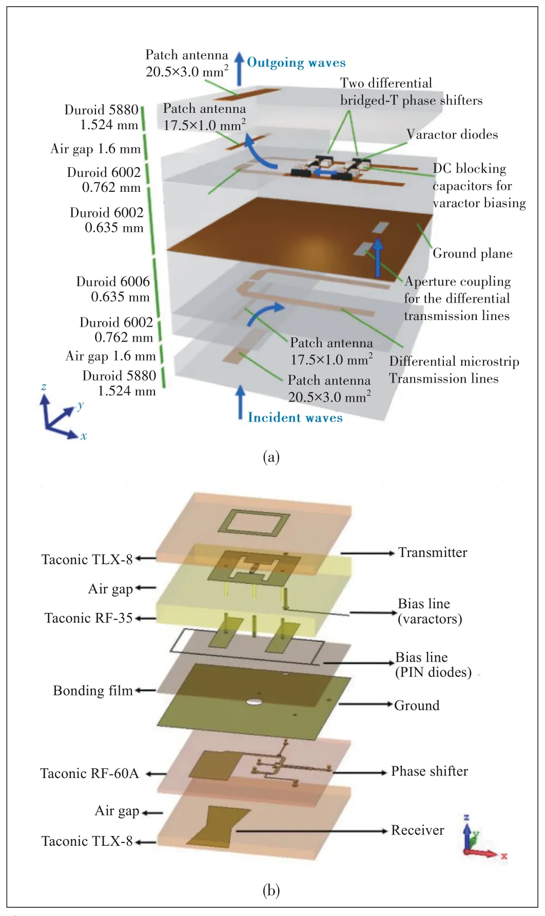
▲Figure 5.Transmissive reconfigurable intelligent surface (RIS) ele⁃ment designs with 360° phase controlling:(a) two cascaded bridged-T phase shifters in Ref]5];(b) a 180° analog phase shifter combined with 1-bit phase shifter in Ref]9]
An element with continuous phase controlling can be found in Ref]5],and the element structure is exhibited in Fig.5(a).The microstrip-slot coupling structure is adopted in this design to transfer energy between Rx and Tx,which are both stacked dipole patches.Two cascaded bridged-T phase shifters loaded with six varactor diodes are selected to reconstruct the trans‑mission phase.It is worth mentioning that the stacked dipole patches are fed by the differential microstrip transmission lines,and two rectangular gaps are opened in the ground to transfer the differential signals.The simulated results demon‑strate that the element is capable of a phase tuning range of over 400°,with the transmission loss maintaining below 3.6 dB.
Some attempts have been done in Ref]9]to reduce the ele‑ment transmission insertion loss,and the schematic of the pro‑posed element is displayed in Fig.5(b).By combining a 180°analog phase shifter loaded with varactor diodes and a 1-bit phase shifter loaded with p-i-n diodes,the element is able to shift its transmission phase over 360°.By utilizing the simple current reversal mechanism,the 1-bit phase shifter circuit is integrated with the Tx patch instead of using a complex phase shifter,and the element insertion loss is effectively reduced.It is indicated that the simulated transmission insertion loss ranges from 0.95 dB to 1.35 dB at 5.6 GHz,with a 3-dB trans‑mission loss bandwidth of 16.7%.
In Ref]6],an element consisting of three resonant structures is exhibited.As displayed in Fig.6(a),two microstrip patches embedded with varactor diodes operate as two resonant struc‑tures.They are positioned on the two sides of a ground plane and coupled by a slot aperture.A varactor diode is inserted into the slot to form the third resonant structure.Therefore,the resonant frequency of the radiating patch could be manipulated by chang‑ing the biasing voltages applied on the varactor diodes.The mea‑sured phase shift ranges at 5.5 GHz is only 245°while the trans‑mission insertion loss reaches up to 2.7-5.7 dB.
Based on the stacked FSS structure,a continuous phase controlling RIS element at C band is detailed in Ref]13].As illustrated in Fig.6(b),it is made of a five-layer stacked square slot and an extra layer to accommodate the biasing cir‑cuits.Each square slot FSS is loaded with two surfacemounted device (SMD) varactors and functions as a band-pass filter.This means if the frequency of the incident wave is close to the resonant frequency of the FSS,it can propagate through FSS.By adjusting the values of the SMD varactors,the resonant frequency of the square slot varies,and thus the phase response of the propagating wave can be controlled.Thanks to the cumulative effects of the phase response of each FSS,the stacked FSS element can generate a phase tun‑ing range of 360° when the transmission insertion loss is within 3 dB in simulations.However,the operating bandwidth is only 90 MHz.
4 Conclusions
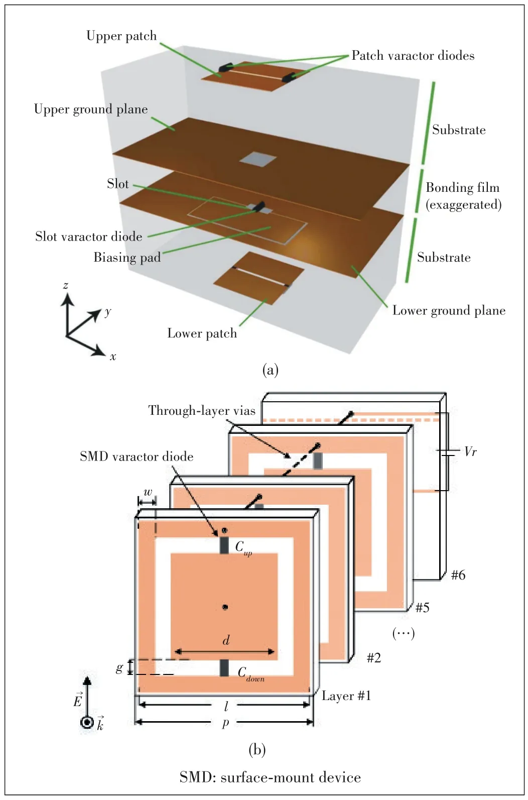
▲Figure 6.Transmissive reconfigurable intelligent surface (RIS) ele⁃ment designs with 360°phase controlling:(a)an element with three reso⁃nant structures in Ref]6];(b) 5-layer stacked frequency selective sur⁃face(FSS)structure in Ref]13]
Recently,the RIS technology develops rapidly as the de‑mands of low-cost and low power consumption beamforming systems increase.Various application scenarios of the RIS have been explored,such as wireless power delivery[35],wire‑less coverage extension[36]and efficient channel estima‑tion[37].Specifically,the transimissive RIS has found its place in the indoor signal coverage.This paper reviews some of the latest developments of the transmissive RIS designs.The design methods utilized in most transmissive RIS de‑signs are briefly introduced.Several representative designs with different phase resolution and polarization capabilities are presented and discussed.Currently,great efforts are be‑ing made to push the frequency frontier of the RIS technol‑ogy towards the W and THz bands.Active devices are being incorporated to achieve signal boosting capability.Various RIS-aided systems are being developed to demonstrate the potential applications of the RIS technology in future wire‑less communications.It is believed that the RIS has a prom‑ising future.
- ZTE Communications的其它文章
- Editorial:Special Topic on Reconfigurable Intelligent Surface (RIS)
- Recent Progress in Research and Development of Reconfigurable Intelligent Surface
- Some Observations and Thoughts about Reconfigurable Intelligent Surface Application for 5G Evolution and 6G
- New Member of ZTE Communications Editorial Board
- IRS⁃Enabled Spectrum Sharing:Interference Modeling,Channel Estimation and Robust Passive Beamforming
- Resource Allocation for Two⁃Tier RIS⁃Assisted Heterogeneous NOMA Networks

