
Analysis of optical emission spectroscopy data during silicon etching in SF6/O2/Ar plasma
2022-01-10 14:51:36DongHwanKIMJeongEunCHOIandSangJeenHONG
Plasma Science and Technology 2021年12期
Dong Hwan KIM, Jeong Eun CHOI and Sang Jeen HONG
Department of Electronics Engineering, Myongji University, 116 Myongji-ro, Yongin-si, Gyeonggi-do,Republic of Korea
Abstract Silicon etching is an essential process in various applications,and a major challenge for etching process is anisotropic high aspect ratio etching characteristics.The etch profile is determined by the plasma parameters and process parameters.In this study,the plasma state with each process parameters were analyzed through the optical emission spectroscopy (OES) plasma diagnostic sensor by both chemical and physical approaches.Electron temperature and electron density were additionally acquired using the corona model with OES data that provides chemical species information, and the etch profile was evaluated through scanning electron microscope measurement data.The results include changes in profile with gas ratio, bias power, and pressure.We figure out that factors like ion energy and ion angular distribution as well as chemical reaction affect the anisotropic profile.
Keywords: silicon etching, profile, optical emission spectroscopy, plasma in-formation, corona model
1.Introduction
Silicon etching is a critical process in the manufacturing of a semiconductor chip on a silicon substrate, and it strongly affects the subsequent material deposition and ion implantation processes.The characteristics of the resulting etch,such as wafer uniformity, etch rate, and profile, can be varied by the plasma state.Various researchers have investigated the optimization of etching characteristics by combining the various etching gas mixtures to improve it [1–3].The development of the through-silicon-via technology for stacked dynamic random-access memory (DRAM) revolutionized the storage capacity limitations in a restricted form factor [4].With the development of more advanced devices,the etching process faces more complex challenges [5, 6].One of the most well-known challenges is high aspect ratio(HAR) silicon etching, which is necessary to form sufficient capacitance and interconnections in the DRAM stacks [7, 8].In addition,it became necessary to isolate individual pixels in complementary metal oxide semiconductor (CMOS) image sensors and to achieve shallow trench isolation in CMOS to prevent electrical interference between devices [9, 10].For HAR etching, it is imperative to form narrow and deep trenches while maintaining a steep anisotropic profile.As the aspect ratio increases with device miniaturization, more precise control of the etch profile is necessary,and an aspect ratio dependent etching lag control is required [11].
Anisotropic HAR etching is plagued by numerous challenges such as bowing and necking, which become more noticeable at higher aspect ratios.It is essential to prevent these challenges from forming.Several reports suggested that these profile issues arise from charging effects and ion angular distribution [12–14].Numerical simulation modeling has also been employed to understand the phenomena of wafer charging during the etching and wet-spin processes[15,16].Duraset alanalyzed the ion angular distribution using a simulation of a plasma thruster [17].Donkóet alconstructed an analytical model of oxygen CCPs to investigate and understand the energy and angular distribution functions [18].Martinset alconstructed a simulation model to predict the trench profile by utilizing the experimental data [19].Recently, many studies have performed plasma diagnostics usingin situsensors[20–22].Although various approaches with cryogenic temperatures and sidewall passivation have been utilized[23, 24],achieving anisotropic HAR etching is still a major challenge.In order to overcome this hurdle, research has been conducted with various approaches until recently.Duet alcorrelated the effect of parameters with scanning electron microscope(SEM)data and etch rate [25].Hanet alanalyzed the effect of parameters using Johnson–Cook fracture model and energy flux in deep trench isolation structure [26].Salehiet alanalyzed through SEM by utilizing information on chemical reactions and radicals that may occur in the process [27].
In the current study, we performedin situmonitoring of silicon trench etching using SF6/O2/Ar plasma and optical emission spectroscopy (OES)to measure the anisotropic etch profile.The OES data are used to identify the atomic/molecular spectroscopic transitions in the excited state, and the electron temperature and electron density were calculated using selected wavelengths’OES data to interpret the plasma state[28,29].The processed OES data containing the plasma information (PI) was then compared to the cross-sectional images of etched profiles collected using a SEM.In section 2,a theory for the plasma diagnostics and a method for deriving plasma parameters from selected emission lines are provided,and section 3 presents the experimental conditions for the etch process on 300 mm production and metrology tools.Section 4 provides the etch profile results as a function of the process conditions.Finally, the transition of the etch profile is analyzed using the OES data and the plasma parameter information.
2.Theory and diagnostic methodology
Plasma is the fourth fundamental state of matter and is composed of gaseous ions and atoms with free electrons.It can be generated by heating or by the collision of accelerated electrons within an electric field.It is worthwhile to understand the behavior of the electrons and chemical species in plasma.
One of the features of plasma is light emission through glow discharge, which is related to the energy levels of the atomic or molecular species.In order to guess how many ions and radicals are in the chamber, the amount of transition of the energy level in each chemical is important, and information on the energy transitions can be observed using OES.To interpret the OES data,an optical sensor that diagnoses the plasma state was used to measure the light emitted from the SF6/O2/Ar plasma, and a spectroscopic theory of atoms and molecules is introduced for the gases used in this study.
The calculations of the electron temperature and electron density in the plasma were obtained using the intensity ratios of the selected emission spectrum lines.Table 1 shows the primary chemical species generated through the chemical and physical reactions during silicon etching using an SF6/O2/Arplasma.The plasma arises from the electron impacted dissociation of SF6and O2gases, according to equation (1)
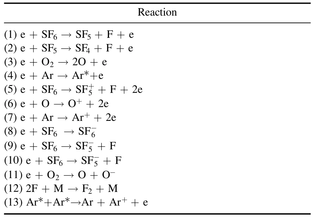
Table 1.Main reactions in SF6/O2/Ar plasma.
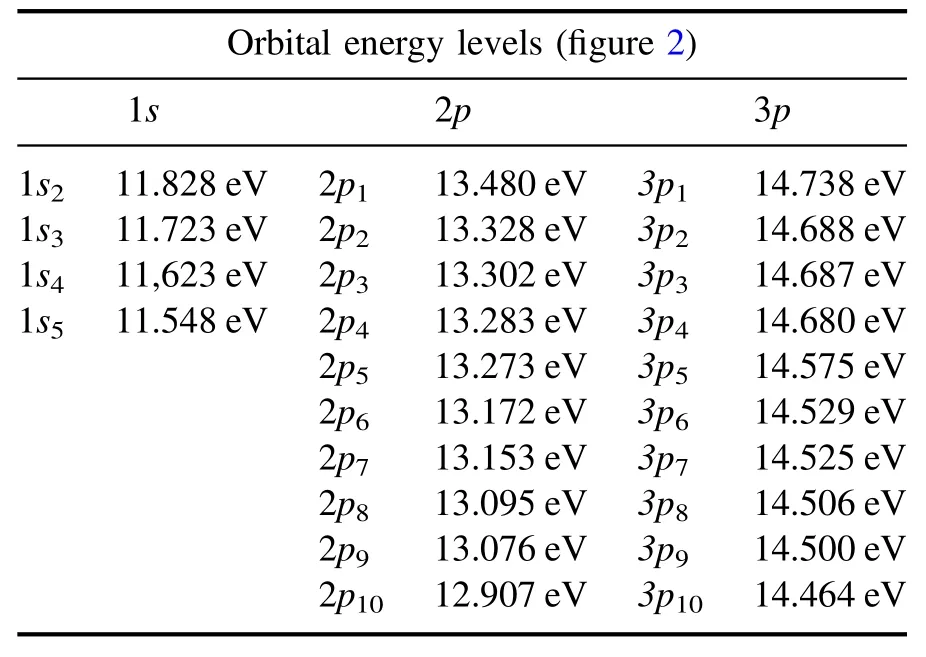
Table 2.Energy levels for Ar atoms according to the Paschen notation.
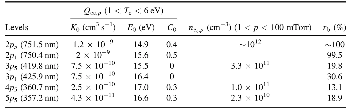
Table 3.Information of the Ar np level (J=0).
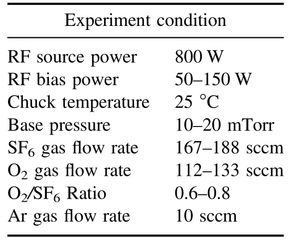
Table 4.Recipe for HAR silicon etch.
Dissociated radicals formed from the energetic electron collision are ionized and attach to electrons,and the resulting fluorine and oxygen radicals can chemically react with the exposed silicon surface.The reaction of silicon with fluorine atoms forms SiF4, an etch by-product, and the oxygen atoms form SiO2on the exposed silicon surface.Argon gas does not chemically react with the other atoms, but it provides an augmented free electron to the plasma through Penning ionization and an excitation generated by the increased electron collision.In this way, bound electrons of various chemical species in the plasma become excited and emit light during relaxation.In the case of an atom,the emitted energy is equal to the difference between the predetermined energy levels,giving rise to light with a characteristic wavelength.In the case of molecules, light is emitted in the form of a band,where the arrangement of bonded atoms is important, and is more complicated because not only are the electrons excited,but there are also the vibration and rotation of the electrons in the molecules.
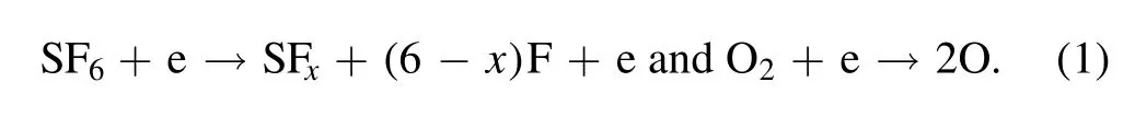
A spectroscopic analysis can determine the relative amounts of radicals, atoms, and molecules present in the chamber through light emission.Although the naked eye can observe the apparent plasma light emission through a sidewall viewport of the process chamber, a spectrometer with a diffraction grating can spread the plasma discharge into the separated wavelengths of light.The full spectrum for SF6/O2/Ar plasma and the representative wavelengths used in the OES analysis are shown in figure 1.
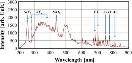
Figure 1.Main peak for the chemical species in SF6/O2/Ar plasma.
Band-shaped peaks are present due to the SFxradicals and species related to etch by-products, SiF4and SiO2.The band emission at 450 nm is related to pure SiO2[30],and the broad band at 300–350 nm corresponds to SFxradicals [31].OES is a non-invasive plasma monitoring technique,and it is useful for identifying the chemical information in the plasma.However, the interpretation becomes more difficult when the plasma also includes several kinds of process gases and etch by-products in the gas phase.OES also has a limitation that it can only provide the local information at installed area such as an area viewed from the sidewall viewport of the chamber.It is difficult to collect the information on the wafer surface and plasma sheath,so the data must be inferred and analyzed through species information collected at the viewport location.Therefore,meaningful information about the process can be obtained by analyzing both the input recipe and the OES information.It is possible to understand the reactions occurring in the chamber overall, not in a local position, by determining the electron temperature and electron density that exists in the plasma.
A common method to measure the electron temperature and electron density of a plasma is with a Langmuir probe measurement [32–34].The Langmuir probe applies a small sinusoidal voltage at the probe tip to diagnose the electron temperature and plasma density.When the probe tip has a floating potential through a sinusoidal voltage, the current coming from the plasma contains various harmonic components because it is nonlinear, and this signal is analyzed to determine the plasma parameters.One disadvantage of the Langmuir probe measurement is that the high potential applied to probe may perturb the plasma.As an alternative,rare gas can be injected into the process chamber for obtaining the plasma parameters without causing a plasma transformation[35,36].This gas can increase plasma density as well as get PI such as electron temperature and electron density because they do not have chemical reaction with other gases.This method obtains the PI using the line intensity ratio of a specific level of the rare gas.In this study,argon gas was used as the rare gas to derive PI.
The energy levels of an argon atom according to the Paschen notation is presented in table 2, and the typical transition of an excited argon atom reported in the National Institute of Standards and Technology database is shown in figure 2.The physical reactions that can generate the excited species include collision with the ground state and metastable species, where the species gain energy from the radiationdecay of the higher excited states.The depopulation processes include collisional quenching and spontaneous radiation.
To obtain the PI from the OES spectra,a population model with an equal rate balance equation between the generation and depopulation processes for two excited levels is required,and a model that considers all the generation and depopulation processes is called a collisional–radiative model.At low pressures,the model can be simplified by two processes such that the main generation and depopulation processes are caused by the electron impact from the ground state and spontaneous radiation each other.In this study, the corona model is applied to determine the PI from the two excited emission lines of the argon atom.To obtain the plasma parameters, a Maxwellian distribution is assumed, and the electron energy distribution function is changed from a bi-Maxwellian distribution to a Maxwellian distribution as the bias power increases [37].It is important to select the appropriate line of the excited state,and the PI is derived using the line ratios at 750.39 nm for Ar(p21)and 425.94 nm for Ar (p31).The selected emission lines can neglect the effects of metastability because the total angle momentum quantum number is zero (J=0).The electron temperature is obtained without correlation of electron density(independently)using the following equations,and the electron density can be finally obtained with calculated value:
Figure 2.Typical excited state transition of energy levels for Ar atoms in the p2 and p3 levels.
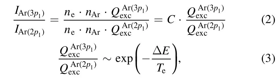
whereCis the partial pressure ratio of the selected lines for the corresponding atoms under the assumption of equal gas temperatures.Since two spectral lines for the same atom were selected,the partial pressures of the two lines are assumed to be the same in this study.QexcAris the excitation rate coefficient from the ground state about superscript’s emission line andnAris the density of the ground state of argon.ΔEis the difference in the electron energy between the two selected lines.The electron density is then calculated independently of the electron temperature when the selected lines are high-lyingnp(n=3,4, and 5) levels.
In these calculations, the electron density was found using the modified equation below.The superscript 1 is for Ar(5p5) and the superscript 2 is for Ar(3p1).Detailed information of the Arnplevel(J=0)is given in table 3[38].
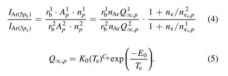
In equations (4) and (5),∞Q p,is the total excitation rate coefficient that includes both the excitation rate coefficient of the transition from the ground state to thenplevel and the partial excitation coefficient from the high-lying level to thenplevel.Apis the Einstein coefficient,npis the density ofnplevel atoms,nec,pis the characteristic density of the electron impact transition to thenplevel,andrbis the branching ratio of the emission line.In the corona model, the total excitation rate coefficient can also be simplified to the transition between the ground state and thenplevel.Therefore, the electron density is obtained with the following equation using the calculated electron temperature:
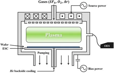
Figure 3.Schematic of an ICP-type 300 mm etcher.
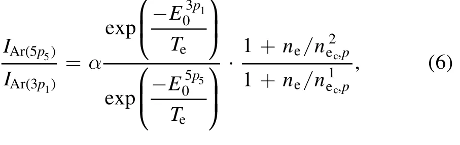
whereαis the correlation factor that considers the branching ratio and the Einstein coefficient, and the energy level of the excited state correlates with the entries in table 2.By selecting the appropriate line, the electron temperature and electron density can be obtained simultaneously.
3.Experiment
HAR etching can be achieved using a highly energetic positive ion bombardment on the silicon substrate, which breaks the silicon bonds and enhances the chemical etching.This is the well-known etch mechanism used in reactive ion etching.In the current study,a Kiyo 2300,a 300 mm wafer processing tool manufactured by LAM Research,was employed,and the schematic diagram of the process chamber is shown in figure 3.
To deliver maximum power, the RF matching unit matches the 50 Ω of preset impedance between the RF power generator and the chamber.When the 13.56 MHz of RF source power is connected to the three-turn type inductive coils,high-density plasma is generated.Like many production tools,it contains a process gas supply system that can deliver multiple gases controlled by mass flow controllers, the base pressure is controlled with a turbo molecular pump with a pendulum control valve.An electrostatic chuck holds the wafer with a backside helium flow to maintain a uniform temperature.The process recipe that was developed for this research consists of two main steps:a breakthrough(BT)step and a main etch (ME) step.The BT step includes anin situdry cleaning of the native oxide and removes any contaminants, and the ME performs the silicon etch using the reaction between the fluorine-based compounds and the silicon substrate to form the volatile product SiFx, and performs the Ar sputtering.
Sulfur hexafluoride(SF6)was adopted for the silicon etch chemistry on account of the accessibility of the gas and the environmental regulations in the university research environment.Since SF6gas demonstrates typical isotropic etch characteristics for etching silicon, it is a difficult challenge to develop a process recipe to obtain vertical etch profiles.To alleviate the concerns of the gas chemistry in the HAR etch,an augmentation of the mixture gas containing O2and Ar was considered.A sidewall passivation layer of SiO2helps to prevent lateral etching by reducing the fluorine–silicon reaction on the trench sidewall as the etch progresses[39], but the etch profiles varied with the gas flow ratio of SF6/O2.Thus,an analysis of the etch profiles with respect to the change of the gas flow ratio was required.As mentioned previously, Ar gas was included to increase the electron and radical density via Penning ionization and excitation.The increased electron density contributes to the energetic ion bombardment on the silicon surface where the velocity is higher than the Bohm velocity passing through the sheath.
During the etch process,two kinds of data were collected in real-time.The first was the equipment status variable identification data, which contains the equipment operating conditions according to the current process recipe using the preinstalled equipment status monitoring sensors.The second was thein situsensor data that contains information about the plasma and wafer interaction.The Ocean Optics S2000 spectrometer that was used has 42 mm of input focal length,68 mm of output focal length, and 14 different gratings.The spectrometer detector has a high-sensitivity 2048 element charge-coupled device array and covers the range of 200–900 nm with resolution of 0.338 nm.By applying the emission spectral line ratio method of the two selected wavelengths for Ar to the equations, the electron temperature and density could be calculated during the process.All these data are automatically stored in a database with a frequency of 1 Hz.
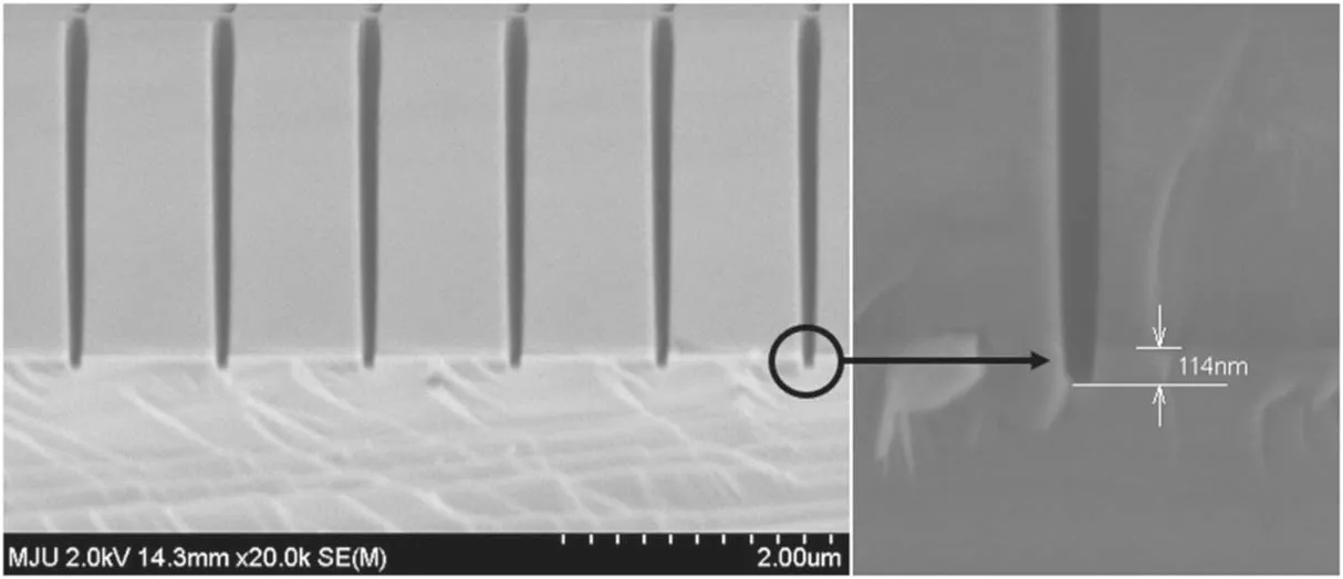
Figure 4.SEM measurement of an SiO2/Si sample.

Figure 5.Results of silicon etching as a function of the gas ratio; (a) SEM measurements and (b) plot of the etch depth and width.
The process parameters of interest are the gas flow ratio,RF bias power, and chamber pressure.The RF source power was fixed at 800 W, and the ratio of SF6to O2was varied to investigate the vertical etch profile as a function of the oxygen passivation.The RF bias power facilitates the ion bombardment for physical etching,and the chamber pressure was varied to determine the change in the etch profile as a function of the plasma density.Detailed information about the process recipe is presented in table 4.After performing the BT step for 30 s,the ME step immediately began without breaking vacuum for a process time of 180 s.The etch profiles were investigated using an SEM cross-sectional image with a magnification of 20 000.A 2×2 cm2SiO2/Si wafer coupon with a bar and hole type pattern was carefully placed in the center of a 300 mm bare silicon wafer used as a coupon sample carrier.Silicon oxide,used as an etch mask,was deposited to a thickness of 2400 nm on the silicon to form the pattern and was then slightly overetched by 114 nm,as shown in figure 4.The maximum trench width was 200 nm and the etch profile was analyzed for 200 nm of the bar pattern.Since the patterning took place with a coupon mounted on a silicon substrate, there is a possibility that the silicon was etched not only in the trench, but also on the entire 300 mm wafer.
4.Result and discussion
4.1.Gas ratio
The data were collected with a range of 0.6–0.8 for the O2/SF6ratio,and the etch profile including the etch depth and bottom width was analyzed using SEM and numerical plotting,as shown in figure 5.The process was carried out with a bias power of 100 W and a fixed pressure of 10 mTorr(table 4).During the etching process with a mixture of SF6and O2gases, it is known that O radicals generated by the plasma combine with Si and form SiOxFyon the sidewall[40].The etch profile therefore becomes more anisotropic due to the passivation of the O2gas with an increase in the O2ratio (figure 5(a)).The bottom width decreases due to an anisotropic change in the etch profile as shown in figure 5(b).An increase in the etch depth was achieved by increasing the oxygen ratio.To confirm the relationship between the gas ratio and the etch profile, OES sensor data were analyzed to monitor the change of the plasma characteristics, such as radical formation and electron temperature.
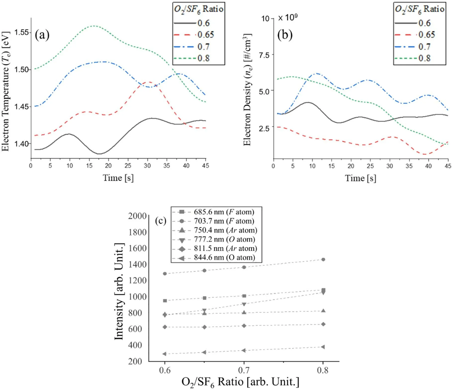
Figure 6.Physical and chemical information about the plasma as a function of the gas ratio; real-time data of (a) electron temperature,(b) electron density, and (c) main peak for the process.Note that the fast Fourier filtered data are presented for (a) and (b).
The OES data and the electron temperature and electron density that were calculated during the process are shown in figure 6.Langmuir probe is the most common sensor to acquire exact value as mentioned before, but there are some problems to utilize it.The equipment used have chamber liner in plasma chamber and mesh on view port of the chamber for electromagnetic shielding.Even if we remove them all and install Langmuir probe, we think the result of PI are quite different between by derived from corona model and Langmuir probe because the absence of components causes the change of shape of plasma or deformation of the plasma.Based on the studies that prove validity of method through Langmuir probe [41, 42], we applied this method although it has uncertainty.
Therefore, a qualitative analysis of the OES data for the electron temperature and electron density is more beneficial than a quantitative approach to explain the observations, as shown in figures 6(a) and (b).It can be seen that the timeseries data for electron temperature does not change significantly with the change of the gas ratio, but the electron density further increases.This is because the electron density increases as the electronegativity decreases [43, 44].When the gas ratio increased, the electron temperature slightly increased,and an increase of the gas ratio caused an increase in the intensity of the SFxradical because SFxradicals emit light with shorter wavelengths than SiO2, indicating that SFxrequires a collision with electrons at higher energy.As more dissociation occurs, more F radicals are produced, which is consistent with figure 6(c) that shows the intensity changes for a single neutral atom.The intensity of both F radicals and O radicals also increased,which is consistent with a previous report [40] that indicated the formation of a sidewall passivation was caused by an increase of O radicals.
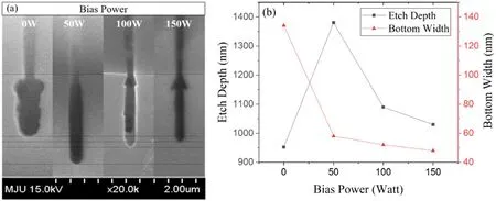
Figure 7.Results of silicon etching as a function of the bias power; (a) SEM measurements and (b) plot of the etch depth and width.
These contributed to an improvement of the etch rate and the anisotropic profile through a chemical reaction according to the gas ratio.However,an arrow-shaped profile appeared at the entrance of the trench when the experiments were conducted to vary the ratio.It is possible that the arrow-shaped profile was induced by the increased ion collisions inside the trench that contained a weaker sidewall protective layer, and the PI is helpful to investigate this effect.Given that the temperature of the chamber is only 60 °C, the thickness and hardness of the SiO2sidewall passivation formed by the diffusion of O radicals is inferior to a layer formed at higher temperatures.Argon ions are generated when argon gas is injected to increase the plasma density and sputtering to the bottom of the trench beyond the sheath.At that time, the energy of the incident ions is very high since the bias power is high.The electron temperature increases as the gas ratio increases, which leads to an increase of the energy flux of incident ions and an increase in the etch rate.In addition,the abnormal profile observed in the SEM images can be also explained by this process, because ions that pass through the sheath collide with each other,which results in bombardment at an angle.From the perspective of the ion angular distribution, the incident ion injection angle becomes wider when ions collide with an ion of heavier molecular weight or atomic weight.In the SF6/O2/Ar plasma, heavier radicals exist with a higher kinetic energy than the binding energy of SiO2.Thus, the ions that are initially traveling straight to perform the physical etching collide with ions or radicals in the plasma and the angle is distorted, resulting in an arrowshaped etch profile.On the other hand,more SiO2passivation layers are formed on the sidewall as the O2ratio increases,preventing sidewall etch, and consequently sharpness at the upper portion of the profile is improved.The phenomena that collide with ions or radicals in the plasma and the role of SiO2passivation layer affect the arrow-shaped profile.
4.2.Bias power
The process changes resulting from varying the RF bias power with a fixed gas mixture ratio were evaluated.It was confirmed that the bias power generates an arrow-shaped profile, as mentioned in the above analysis of the gas ratio variation.Bias power is the most likely source of the arrowshaped profile because it controls the ion energy via self-bias.When the bias power was increased from 0 to 150 W,the etch characteristics changed, as shown in figure 7.Without RF bias power, an isotropic etch profile was obtained with a shallow etch depth and a large amount of lateral etching.Without bias power, the chemical etch mechanism is more dominant than the physical etch mechanism, resulting in an isotropic profile and a wide bottom width.As the bias power increases, the etch rate tends to increase due to the increased ion bombardment [45].
The etch rate increased when the applied RF bias was increased from 0 to 50 W, but an unexpected decrease in the etch rate was observed when increasing the RF bias power from 100 to 150 W.The arrow-shaped profile was apparent with the increased RF bias power.It is likely that the etch depth was decreased due to the deficiency of ions near the trench bottom, and the arrow-shaped profile was reinforced by the energetic ion bombardment corresponding to the increase of bias power, although the physical etch of the wafer surface was enhanced with the increase in bias power.
To interpret the etch results,the electron temperature and electron density derived from the OES data were considered,as shown in figure 8.The bias power is used only for controlling the ion energy, but the electron temperature and the electron density changed with the bias power.From figure 8(a), when there is no bias, the electron temperature is low, and the electron density is high.As the bias increases,the electron temperature increases, and the electron density decreases.This effect can be understood because the device operates in inductive mode (H-mode) rather than capacitive mode (E-mode) due to the high source power of the antenna coil applied for the plasma formation.The RF power applied to the electrode vibrates the sheath,generating a collision-less heating, which can heat the electrons as well as produce ohmic heating and collisional heating from the electric current flow.Electron heating by such electrode power may cause an increase in the electron energy distribution and electron temperature [46].
The decrease in the electron density can be explained by the positive ion density.As shown in figure 8(b), when zero bias power was applied, the emission intensities related to F,O, and Ar atoms were higher than when RF bias power was applied.There were a few positive ions that bombarded the target through the sheath because there was a small self-bias effect as well as an effect of electron heating by the external power.Therefore,it was possible to obtain isotropic results as imaged by SEM.In addition, the OES intensity at short wavelengths increased as the applied bias power increased.An increase of the intensity at short wavelengths means that the chemicals are more susceptible to ionization or dissociation because the electron temperature is higher.Therefore,more positive ions are generated due to the collision between molecules and electrons, and there are more energetic ions sputters beyond the sheath.As energetic ions increase, ions moving toward the sheath beyond the plasma bulk with energy above the Bohm velocity increase.Accordingly, the density of ions presents in the plasma bulk decreases, which means that the density of ionizable chemicals due to the collision of electrons decreases in the plasma bulk.Therefore,the electron density in plasma bulk, which is an area where the OES optic fiber is facing decreases because the probability of ionization that can occur in the plasma bulk decreases.
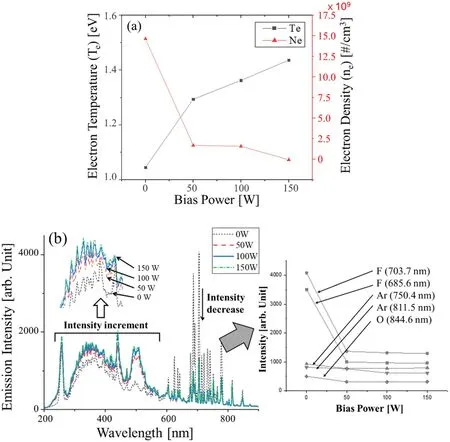
Figure 8.Physical and chemical information about the plasma as a function of the bias power; (a) plot of the electron temperature and electron density and (b) full spectrum OES data.
The arrow-shape profile is then formed by the ion angular distribution and ion energy.As the bias power increases, the incident ions have a higher energy even though they are colliding with the radicals.Therefore,the sharpness of profile becomes stronger as the bias power increases.It can also be interpreted that an arrow-shape profile is formed because high energy ions lose their charge after they collide with the trench bottom or the passivation layer, resulting in partial charging.
4.3.Pressure
Another factor that can determine the energy of the ions, the pressure, was also analyzed.The pressure was studied at two values, 10 and 20 mTorr.The results of the pressure change study are shown in figure 9.When the pressure was increased,the etch rate increased significantly and the arrow-shaped profile was not formed.The etch profile was anisotropic without an arrow-shaped profile despite the increase of the bottom width.The relationship between pressure and etch rate can be explained by ion flux [47].As the pressure increases,the etch rate should decrease due to ion flux impinging.However, the etch rate increased at 20 mTorr because of the increase in the concentration of F radicals that can react with Si had a stronger effect than ion flux impinging.When the pressure was varied,the overall intensity of the OES spectrum decreased, as shown in figure 10(b).
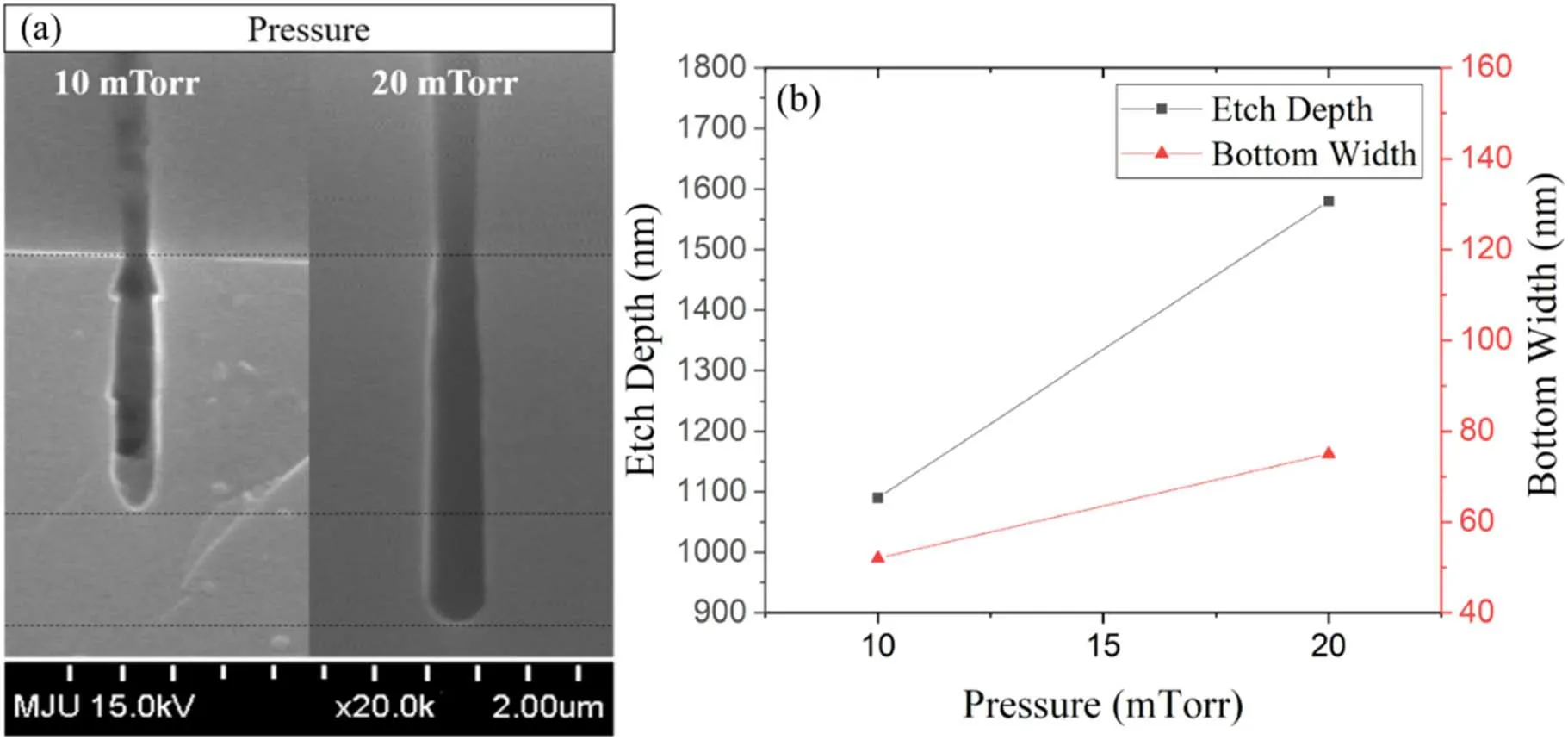
Figure 9.Results of silicon etching as a function of the pressure; (a) SEM measurements and (b) plot of the etch depth and width.
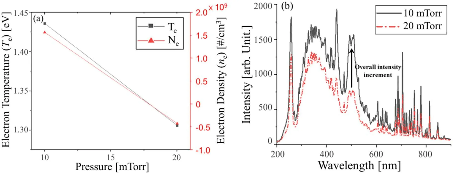
Figure 10.Physical and chemical information about the plasma as a function of the pressure;(a)plot of the electron temperature and electron density and (b) full spectrum OES data.
In addition, as the pressure increased, both the electron temperature and the electron density decreased.At higher pressure, the density of the gas present in the chamber is higher,and the mean free path,the distance at which particles(such as an atom, a molecule, a radical, a photon) do not collide with other particles,decreases.This means that energy loss of electrons with particles occurs before having enough energy in the plasma, and this energy can be expressed as a temperature.So, the electron temperature decreases.As the density of electrons that do not have sufficient energy to ionize neutral atoms increases,the electron density decreased,as shown as figure 10(a).In addition, the probability of a collision between species increases as the pressure increases.Since the bias power is kept constant, the physical etch will proceed beyond the sheath by ions.Sheath thickness becomes thinner and ions with more than Bohm velocity decrease as the pressure increases.Therefore, rather than creating an arrow-shaped profile by hitting the sidewall with high energy ions, physical etch proceeds vertically on the surface where bonding is broken through chemical reaction.Overall, the etch rate increased while the most ideal anisotropic profile was maintained because the number of ions bombarded to the trench bottom increased.
5.Conclusions
As the etching process difficulty increases, maintaining the anisotropic etch profile as well as the etch rate is emerging as an important aspect in silicon etch.Some applications require anisotropic HAR etch,but it can be largely impacted by both physical causes like ion incident energy and charging effect and chemical causes like radical density.In this study, etch process characteristics observed by SEM were evaluated through analyzing chemical and physical phenomena occurred in the HAR etch process using diagnostic sensors and derived models.We used OES owing to the advantage of not making the plasma perturbation unlike Langmuir probe.OES is a well-known diagnostic sensor that basically provide information about chemical species, but physical information can acquire at the same time by utilizing the rate equationbased corona model in this study.It was analyzed from the plasma point of view process along the change of parameters such as gas ratio, bias power, and pressure.As a result, a change of cross-section profile occurred due to the influence of ion energy, and finally, an arrow-shaped profile issue appeared according to the process parameters.The arrowshaped profile was remarkable, which was influenced by incident ions passing through the sheath as the gas ratio increased, the bias power increased, and the pressure decreased, respectively.Through SEM measurement data,sensor data,and PI data,the profile issue according to the gas ratio change can be explained that it is due to the change in the collisional angle of incident ions with relative change in the chemical species existing in the plasma.Also, change of the ion incident energy and wafer charging is the cause as well as the ion angular distribution of incident ions in the plasma in case of bias power and pressure.We finally found that as the information of electron temperature, electron density, and radicals changes, the anisotropic profile was no longer formed.It was also possible to understand the change of etch depth and selectivity result through plasma analysis with the diagnostic sensor.It was difficult to analyze process issues solely from the post-process measurement results, but when coupling with the plasma diagnostic sensor,meaningful insights were obtained.Profile analysis should take both lateral and vertical characteristics into account,so it is necessary to analyze both chemical and physical characteristics of plasma.However, since OES is not a sensor that provides a quantitative information, it will be more useful for plasma analysis if diagnostic sensors that does not deform the plasma state are used together.
Acknowledgments
This work was supported by the Koran Ministry of Trade,Industry & Energy (MOTIE: GID: 20006499) via KSRC(Korea Semiconductor Research Consortium) support program.Authors are grateful to Prof G H Kim at Seoul National University for his leading a research project team and numerous technical discussions and staff of semiconductor process diagnosis research center (SPDRC) at Myongji University for maintaining high standard equipment and facilities.
ORCID iDs
 Plasma Science and Technology2021年12期
- Plasma Science and Technology的其它文章
- A study on nuclear analysis of the divertor region of the CFETR
- Evaluation of gases’ molecular abundance ratio by fiber-optic laser-induced breakdown spectroscopy with a metal-assisted method
- Thermophysical properties of pure gases and mixtures at temperatures of 300–30 000K and atmospheric pressure:thermodynamic properties and solution of equilibrium compositions
- Plasma treatment for enhancement of the sorption capacity of carbon fabric
- Parametric study of high-frequency characteristics of plasma synthetic jet actuator
- Energy properties and spatial plume profile of ionic liquid ion sources based on an array of porous metal strips