Adverse Effect of Inappropriately Implementing Source-isolation Mitigation Technique
DING Lili, CHEN Wei, WANG Tan, XU Jingyan
(State Key Laboratory of Intense Pulsed Radiation Simulation and Effect, Northwest Institute of Nuclear Technology, Xi’an 710024, China)
Abstract: Single event transient (SET) response was compared between various structures considering source-isolation mitigation technique. The simulation results prove the existence of adverse effects. Besides bipolar amplification effects, both drive strength and node capacitance should be considered when trying to improve SET tolerance. Due to the nonuniqueness of related factors, unless one factor is definitely the main contributor, careful consideration and quantitative evaluation are highly suggested before implementing mitigation techniques.
Key words:source-isolation; single event transient; mitigation technique; adverse effects
1 Introduction
As technology of CMOS integrated circuits scales, decreased supply voltage and increased frequency bring an enhanced contribution of single event transient (SET) in combinational data paths to soft error vulner-ability[1-2]. To control the impacts, various radiation hardened by design (RHBD) techniques have attracted much attention. Some techniques have no net effect on the circuit function or logical size. Layout-level RHBD techniques including guard ring[3], guard drain[4-5], pulse quenching effects[6], etc., definitely belong to this category. Circuit-level techniques including dummy gate[7], drain/source extension[8], etc., are supposed to change the circuit schematic, but still have no effect in logical size. Meanwhile, other techniques, including source isolation, are supposed to change the logical size[9-10].
It is well known that RHBD techniques are inclined to bring extra area or power penalty. In fact, not only the common characteristics, bus also the radiation tolerance is not straightforward to get improved. Some studies have proven that pulse quenching effects are very useful in mitigation SET[11]. However, some other reports show only limited or even negative effectiveness[12]. In this study, SET in various hardening structures regarding source isolation were evaluated and compared. From the simulation results, the adverse impacts were confirmed and presented. If implementing the hardening methods without careful consideration or quantitative evaluation, adverse consequence might be reached.
This paper is organized as follows. Section 2 presents the description of source-isolation technique. Section 3 presents the simulation results. The dependence of key parameters related with hardening structures on SET tolerance will be discussed in detail. Conclusions are drawn in Section 4.
2 Description of source-isolation technique
Source-isolation was meant for P-hit (striking at N-well region) SET mitigation. According to Fig.1, an additional serial PMOS transistor is added to the layout, to prevent the holes being injected from the source of the struck PMOS to the active nodes. Thus, the bipolar amplification effects can be suppressed. The newly added transistor can share the same active region with the previously existing transistor, as illustrated in Fig.1b, or else, the transistor can be isolated from the previous existing one, as illustrated in Fig.1c and Fig.1d.
Referring to reference [13], shallow trench isolation (STI) using to isolate the two serial PMOSs will break the parasitic BJT structure, which could weaken the parasitic bipolar effect efficiently. Thus, layout 3 and layout 4 are supposed to be more robust than layout 1 and layout 2.Fig.2b and Fig.2c illustrate two layout designs implementing various source-isolation techniques, from reference [10] and reference [13] accordingly. Comparing to the original layout in Fig.2a, area penalty exists for sure. At the same time, from Fig.2b, the added PMOS reduces the pull-up circuit strength of the circuit. The output will have imbalanced rise and fall times. The design in Fig.2c is supposed to maintain the rise and fall times with balanced pull-up and pull-down circuits.

a—Original layout (layout 1); b—Typical source-isolation layout (layout 2); c—Parallel source-isolation layout (layout 3); d—In-line source-isolation layout (layout 4)Fig.1 Different layout techniques for PMOS

a—INV1, original layout; b—INV2, with source-isolation design; c—INV3, with source-isolation and balanced pull-down circuitFig.2 Different layout techniques for inverter
3 Simulation results and discussion
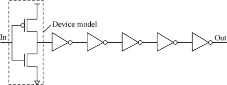
Sentaurus TCAD from Synopsys was adopted in our work to perform structure construction and device simulation. The following physical models were used: 1) band-gap narrowing effect; 2) doping dependent SRH recombination and Auger recombination; 3) the impacts of doping, electric field, and carrier-carrier scattering on mobility. Three-dimensional TCAD simulations were conducted to evaluate the possible adverse effects of RHBD techniques.Fig.3 illustrates the circuit used for the simulation. The first inverter is modeled as TCAD numerical device model, the other 5 stages of inverters are modeled as SPICE model.

Fig.3 Circuit used for simulation
The 3-D TCAD structures and doping distributions were calibrated with a commercial 40 nm CMOS technology, the supply voltage (Vdd) equals to 1.1 V. The substrate depth is set as 20 μm. from Fig.4, spaced N-well and P-well contacts are implemented considering the typical structures in the commercial standard cell library. The TCAD models of inverters are corresponding to the layout techniques in Fig.2, namely INV1_spaced, INV2_spaced, and INV3_spaced.

a—Original layout (INV1_spaced); b—Layout with source-isolation design (INV2_spaced); c—Layout with source-isolation and balanced pull-down circuit (INV3_spaced)Fig.4 TCAD model of inverters with spaced well contacts
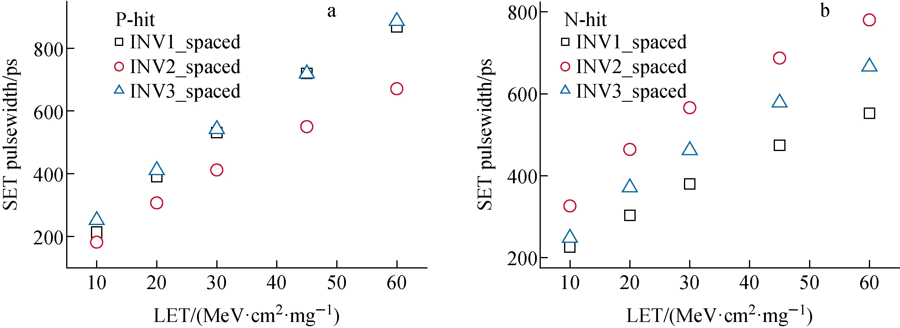
Fig.5 illustrates the simulated SET pulse width when striking at the center region of PMOS drain (P-hit) and NMOS drain (N-hit). from Fig.5a, INV2_spaced does improve the SET tolerance of the inverter chain, P-hit SET pulsewidth gets evidently arrower, which is consistent with the results in references [9] and [13]. However, the P-hit pulsewidth of INV3_spaced is almost the same as that of INV1_spaced. Comparing to INV2_spaced, due to the serial nMOS transistors, the drive strength of INV3_spaced pull-down circuit gets smaller. from Fig.5b, N-hit SET pulsewidth values of both INV2_spaced and INV3_spaced are bigger than that of INV1_spaced. With the introduction of serial PMOS transistor and reduction in pull-up circuit drive strength, N-hit SET tolerance gets weakened clearly. Since the bipolar amplification effects of N-hit can be suppressed in INV3_spaced, INV3_spaced behaves stronger N-hit SET tolerance than INV2_spaced.
From the results in Fig.5, it can be seen that the whole picture is not consistent with the initial estimation. Although source-isolation is meant only for suppressing bipolar amplification effects, along with the introduction of hardening strategies, other parameters related with SET tolerance get changed at the same time. There are at least three key parameters related with P-hit and N-hit SET tolerance. As illustrated in Table 1, suppression in bipolar amplification effects is inclined to increase the SET tolerance. A negative relationship has been confirmed. Decrease in circuit drive strength or increase in node capacitance has negative impacts in SET tolerance. The relationships of circuit drive strength and node capacitance with SET tolerance should be positive and negative correspondingly. The overall impacts depend on the comparative contributions of all the factors. For INV2_spaced layout, increased P-hit SET tolerance is due to the main contribution of bipolar amplification effects. And the corresponding N-hit SET tolerance gets decreased due to the decrease in pull-up circuit drive strength. For INV3_spaced layout, due to the reduced drive strength of pull-down circuit, the overall P-hit SET tolerance gets even worse than that for original INV1_spaced. Comparing to INV2_spaced, due to the suppression in N-hit bipolar amplifications effects, the N-hit SET tolerance is reasonable to be stronger.

Fig.5 SET pulsewidth for inverters with spaced well contacts under P-hit (a) and N-hit (b) conditions

Table 1 Key factors related with P-hit and N-hit SET tolerance of inverters with spaced well contacts
To prove the deduction, layout techniques with guard-ring well contacts are also considered, namely INV1_guard, INV2_guard, and INV3_guard. As illustrated in Fig.6, the well contacts area gets evidently larger than that in Fig.4, the other parts including the PMOS and NMOS arrangements remain unchanged.
Due to the guard-ring protection, the revised layout techniques should have negligible bipolar amplification effects. From Table 2, it can be predicted that the ranks of P-hit SET tolerance should be INV1_guard>INV2_guard>INV3_guard. And the ranks of N-hit SET tolerance should be also INV1_guard>INV2_guard>INV3_guard.
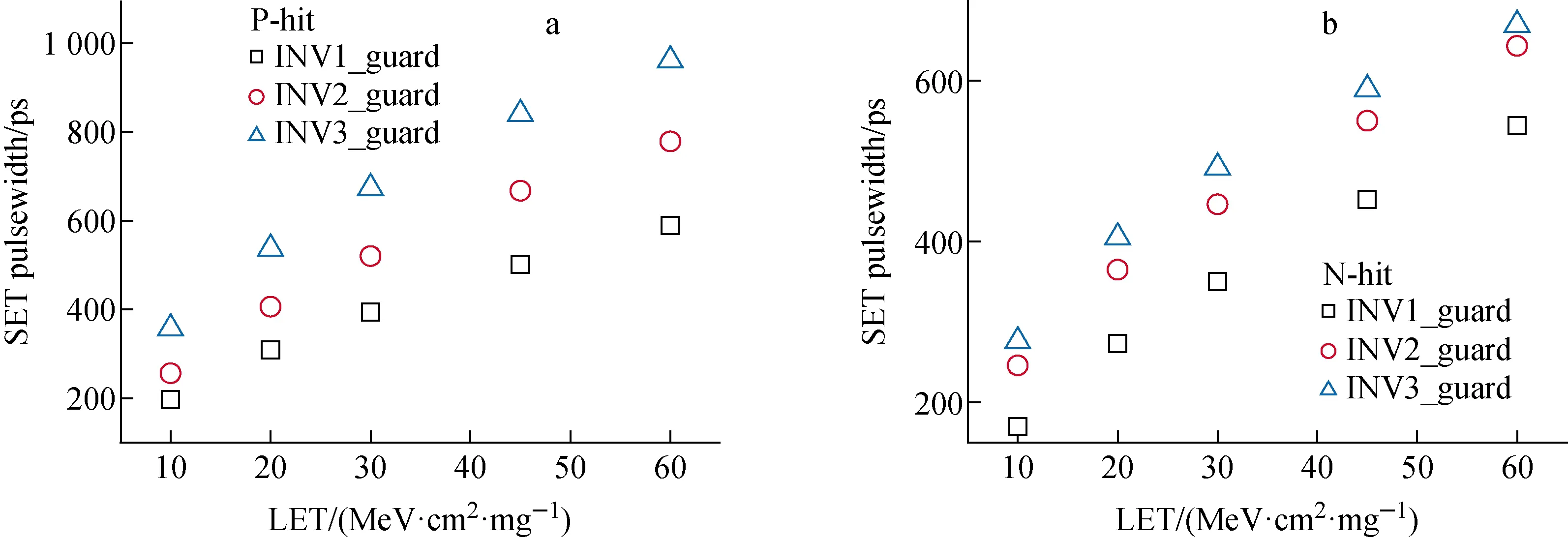
Fig.7 illustrates the simulated results corresponding to the revised layout techniques. As shown in Fig.7a, on one hand, INV2_guard still has better P-hit SET tolerance than INV3_guard, similar to the results in Fig.5a. On the other hand, the SET pulsewidth of INV2_guard gets even larger than that of original inverter layout. For N-hit condition, SET pulsewidth values of both INV2_guard and INV3_guard are bigger than that of INV1_guard. All the tendencies are consistent with the analysis.

a—Original layout (INV1_guard); b—Layout with source-isolation design (INV2_guard); c—Layout with source-isolation and balanced pull-down circuit (INV3_guard)Fig.6 TCAD model of inverters with guard-ring well contacts

Table 2 Key factors related with P-hit and N-hit SET tolerance of inverters with guard-ring well contacts

Fig.7 SET pulsewidth for inverters with guard-ring well contacts under P-hit (a) and N-hit (b) conditions
Furthermore, as illustrated in Fig.8, we keep controlling the factors to propose revised layout designs based on source-isolation technique but with constant logical size, namely INV4_spaced and INV4_guard. From Table 3, INV4_spaced and INV4_guard are supposed to have the same N-hit transient response as the original inverters (INV1). For P-hit, it is hard to tell if the SET tolerance of INV4_spaced could be better due to the two competitive mechanisms. However, INV4_guard is inclined to have weaker tolerance than INV1_guard. The simulation results show that the P-hit SET pulsewidth of INV4_spaced is almost the same as that of INV1_spaced. And all the tendencies agree with the predictions.

a—Schematic of PMOS transistors; b—Inverters with spaced well contacts; c—Guard-ring well contacts; d—Simulated difference in SET pulse widthFig.8 Layout design based on source-isolation technique with constant logical size

Table 3 Analysis of inverters based on source-isolation technique with constant logical size
From the above analysis and simulation results, source-isolation technique is not for sure to improve the SET tolerance. There are at least three factors affecting the SET response. Only modulating one factor is clearly not enough, unless the factor is definitely the main contributor.
4 Conclusion
SET response was compared between various structures considering source-isolation mitigation technique. For the structures with spaced well contacts, source-isolation does improve the P-hit SET tolerance evidently, due to the domination of bipolar amplification effects. However, the whole picture is not always like this. Although source-isolation is meant only for suppressing bipolar amplification effects, along with the introduction of hardening strategies, other parameters related with SET tolerance get changed at the same time. There are at least three key parameters related with P-hit and N-hit SET tolerance, bipolar amplification effects, drive strength and node capacitance. Suppression in bipolar amplification effects is inclined to increase the SET tolerance. Decrease in circuit drive strength or increase in node capacitance has negative impacts. The results of structures with guard-ring well contacts prove the analysis. All the tendencies agree with the predictions.
Through investigating the layout techniques regarding source isolation, the adverse impacts were confirmed and presented. Besides bipolar amplification effects, both drive strength and node capacitance should be considered when trying to improve SET tolerance. Due to the nonuniqueness of related factors, unless one factor is definitely the main contributor, careful consideration and quantitative evaluation are highly suggested before implementing mitigation techniques.
- 原子能科学技术的其它文章
- H-1NF仿星器标准磁场位形分析与高能量离子运动轨道模拟
- 铀转化生产线含氟废水处理工艺设计
- 在线进样ICP-MS用于239Pu气溶胶活度浓度连续监测技术研究
- Degradation Characteristic of Proton Irradiated 8T CMOS Image Sensor
- Comparative Experimental Study on Space Electrostatic Discharge Effect and Single Event Effect of 130 nm SOI D Flip-flop Chains
- Effects of Electron Irradiation at Different Energy and Fluences on Electrical Properties of InP HEMT Structure

