Testing and Characterization of GaN-based MOSFET at Space Cryogenic Temperature
XIAO Yiping, WANG Yaning, LIU Chaoming,*, ZHANG Yanqing, QI Chunhua, WANG Tianqi, MA Guoliang, HUO Mingxue, LU Yudong, YUE Long
(1.Space Environment Simulation Research Infrastructure, Harbin Institute of Technology, Harbin 150001, China; 2.Guangzhou GRG Metrology & Test Co., Ltd., Guangzhou 510000, China)
Abstract: Deep space exploration applications require electronics which are capable of operation at extremely low temperatures (T<40 K). Based on the application requirements of cryogenic temperatures, the effects of cryogenic temperatures from 15 K to 300 K on GaN-based MOSFET were investigated in this paper. The experimental results show that the saturated drain current and threshold voltage are increased as the device is cooled down to 15 K. Both output characteristics and transfer characteristics are enhanced as temperature decreases. The increase of electron migration rate could be the main reason for the shift of electrical parameters of GaN-based MOSFET.
Key words:GaN; MOSFET; cryogenic temperature; characterization
1 Introduction
GaN, as a typical third-generation semiconductor material, is widely used in increasingly harsh conditions due to wide band gap, high saturation drift speed, good thermal stability and high critical breakdown electric field[1-2]. GaN-based MOSFET not only solves the defect of the traditional GaN HEMT, but also has remarkable temperature characteristics[3], which has been closely noticed by researchers and become the focus of experimental research. For MgO/GaN MOSFET, analysis of the output characteristics and breakdown characteristics from 20 ℃ to 500 ℃ on the device shows that break-down voltage and saturation drain current are hardly reduced within 20-500 ℃[4]. Besides, significant decrease of gate drain at elevated temperature was observed on Pt/Ga2O3/GaN MOSFET relative to a conventional Pt/GaN MOSFET, and MOSFET device operation in fact improved upon heating to 400 ℃. Modeling of the high temperature effect on contact resistance shows that the improvement can be attributed to a reduction in the parasitic resistances present in the device[5]. The influence of temperature on the transient switching rate of GaN-based MOSFET was also studied. AtRG=100 Ω, dVGS/dtincreases as the device is cooled from 100 ℃ to -20 ℃, and the temperature characteristics of GaN devices decrease with the decline of migration rate, which contributes to lower wastage and better transient performance[6].
In space, electronic systems that performing tasks in deep space and icy celestial bodies will be subject to ultra-low temperature environment[7-8]. Operation in the most interesting extra-terrestrial locations requires a spacecraft to be capable of surviving any number of harsh conditions. More efficient and reliable performance of the device functioning at the harsh condition is fully needed[9-11]. However, previous work evaluating GaN-based MOSFET device response has focused primarily on high temperature field, so the study of this device at cryogenic temperatures is indispensable.
In this paper, the GaN-based MOSFET is cooled from 15 K to 300 K by a low temperature test platform. The goal of this research has been not only the assessment of the performance of GaN-based MOSFET for cryogenic operations but also the achievement of a better understanding of the physical mechanism involved with temperature-induced effects in active devices. The response of these devices to extreme environments will contribute to the design and manufacture of GaN-based MOSFET in space applications and demonstrate the viability of their use in future systems.
2 Device under test and experimental setups
N-channel GaN-based MOSFET used in this paper was produced by Ganpower (Foshan) Co., Ltd. The size of the device is 3923 μm×1222 μm, doped material is mainly PAD, top metal layer is AlCu, which contains a very small amount of Cu. The thickness of substrate Si is 280 μm and GaN layer is 20 μm, respectively.
In order to satisfy the requirements of the cryogenic experiment, the liquid helium-free optical window cryostat produced by JANIS was used. This cryogenic system concludes a Sumitomo CH-204N two-stage cold head, with an HC-4A air-cooled compressor, and cools by compressing and expanding helium. About 10-6Pa vacuum and about 15 K low temperatures can be provided without consuming liquid helium or liquid nitrogen. A dual independent channel temperature controller (Cryo.con 22C) was used to monitor and control the temperature of the cold head and the DUT. Temperature readings were taken with a T-type thermocouple mounted in the cold head and a Si diode (Lake Shore DT-670, 1.4-500 K) near the DUT. Pins of the tested sample are connected with the electrical connector so as to realize the test of the electrical performance parameters of the sample. The experimental test set-up is shown in Fig.1.
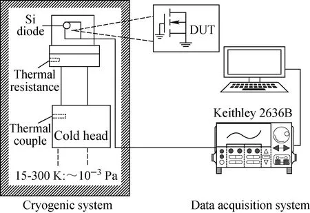
Fig.1 Experimental test set-up
TheI-Vmeasurements including output characteristics and transfer characteristics were carried out by using Keithley 2636B source meter. The device was slowly cooled from 300 K to 15 K over a period of time. As the device cooled, the parameter analyzer sweep was run at 20 K intervals, producing a complete set ofI-Vcurves at each temperature point.
3 Results and analyses
Temperature plays an important role on the electrical and physical characteristics of semiconductor materials. When transistors are exposed to extremely cold temperatures, their operation is altered in the semiconductor material characteristics. The positive outputIDS-VDScurves of GaN-based MOSFET from 15 K to 300 K atVGS=4 V are shown in Fig.2. It can be seen that the drain currentIDSis increased at a given drain voltage, while the drain voltageVDSis degraded at the same drain current with the decreasing temperature. AtVDS=0-5 V, drain currentIDSincreases as enhancedVDS, thenIDSbasically maintains a stable value and positive output curve reaches a saturated state withVDSincreases to more than 5 V.
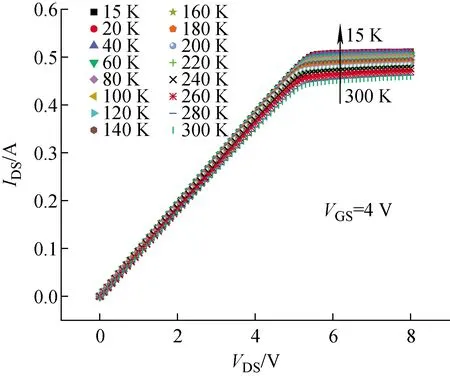
Fig.2 Positive output curves IDS-VDS of GaN-based MOSFET for several temperatures at VGS=4 V
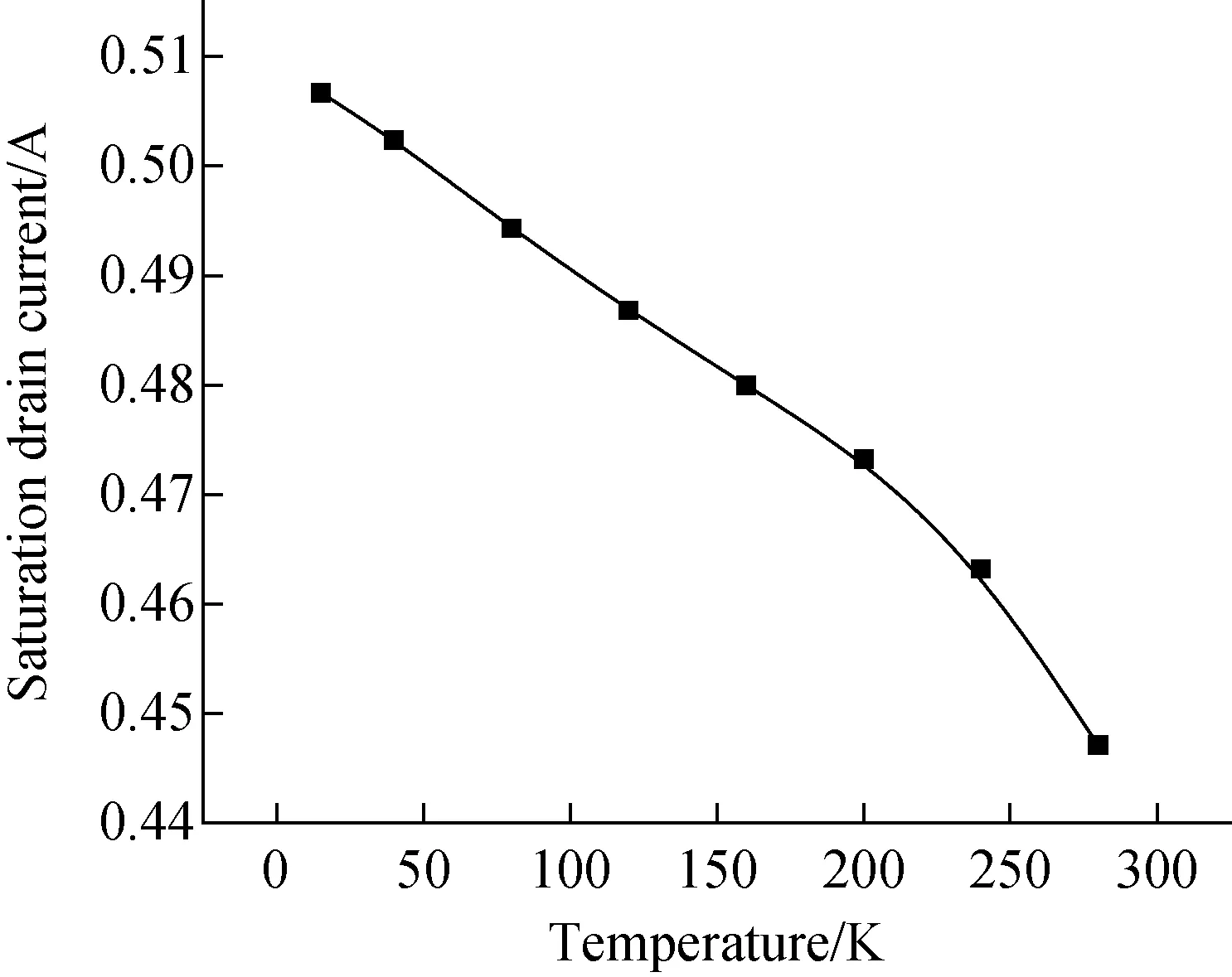
Fig.3 Saturation drain current IDSS of GaN-based MOSFET under different temperatures
The saturated drain currents of GaN-based MOSFET for several different temperatures are shown in Fig.3. There is a sharp rising trend ofIDSSnear the room temperature and the rate of increase inIDSSgradually levels off as the temperature drops below 160 K. The plot can be explained in the following manner. Starting at room temperature, the initial increase in current is on account of a reduction in the electron-phonon scattering rate. However, the increase of impurity scattering rate begins cancel out the electron-phonon scattering effect at lower temperatures[12]. Finally, the electronic migration rate maintains an equilibrium state andIDSSincreases steadily.
RDS_ONof GaN-based MOSFET under different temperatures is shown in Fig.4. Based on previous studies,RDS_ONis defined the ratio of drain voltage to drain current at the unsaturated zone of output curve,RDS_ON=VDS/IDS. It can be seen that the on-state resistanceRDS_ONdecreases over the entire range of the temperature points. The on-state resistanceRDS_ONdecreases by about 6.8% as the device is cooled from 280 K to 15 K, and reaches a minimum value ofRDS_ON=10.48 Ω at 15 K. The lower on-state resistance contributes to the higher drain current, the lower wastage and the better operating characteristics.
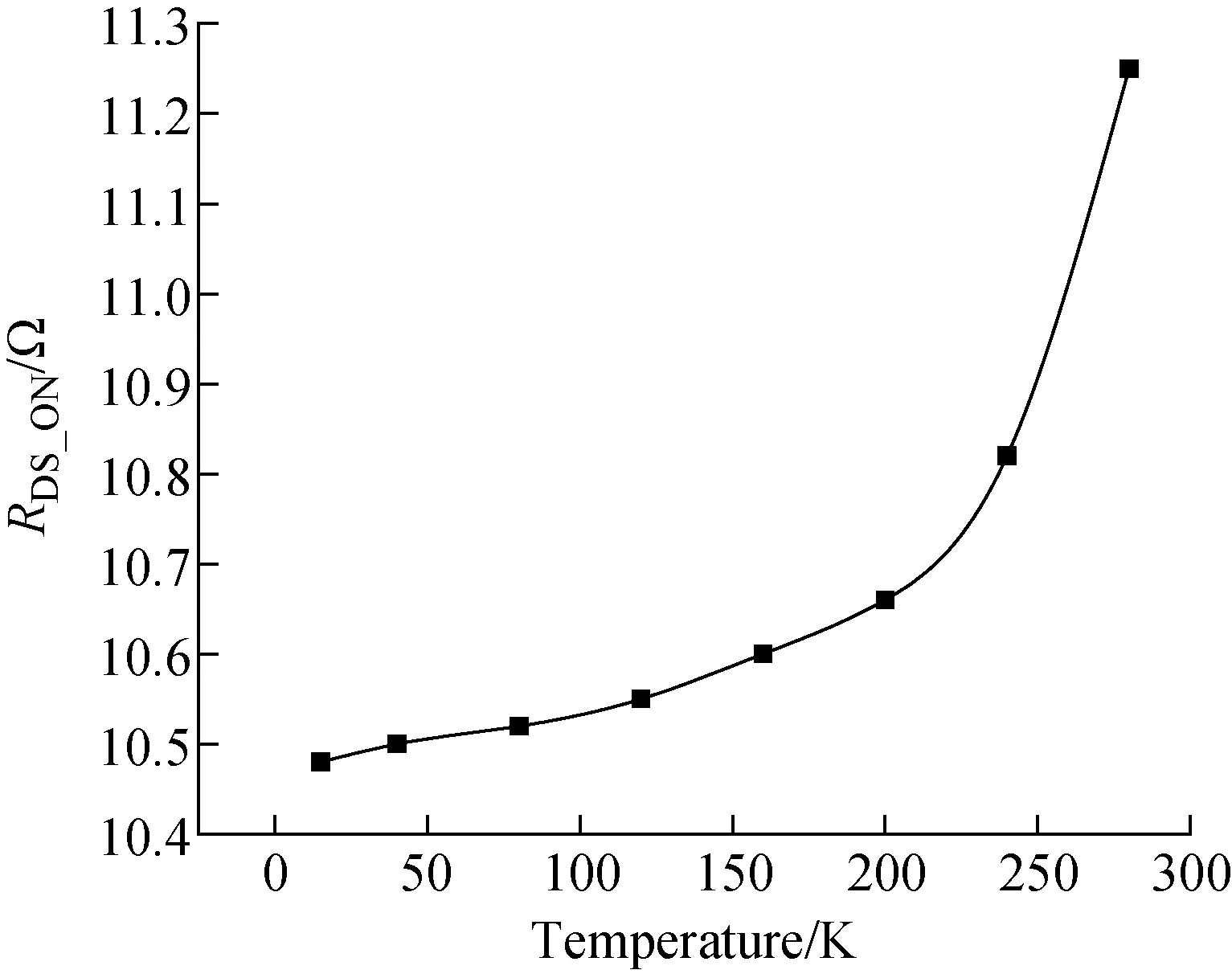
Fig.4 On-state resistances of GaN-based MOSFET at VGS=4 V under different temperatures
The current versus temperature curves in the saturation (VDS=8 V,VGS=4 V) and linear triode (VDS=5 V,VGS=4 V) regions of operation are shown in Fig.5. It is apparent that current in the linear region has very similar temperature dependence to that in the saturation region, indicating that dIDS/dTchanges slightly and self-heating effects barely appear under the experiment.
The trend ofIDS-VGSof the GaN-based MOSFET transfer characteristic curve in the range of 15-300 K is shown in Fig.6. The current shows a similar increase at lower temperature as in the previous output characteristics curve. WhenVGSincrease from 0 to 1 V, the drain currentIDSgrows very slowly, at this time the conversion characteristics are not sensitive to temperature changes, however whenVGSincreases from 1 V to 2 V, theIDSincreases rapidly withVGS, and the rate increases faster when the temperature is lower. Such improvements inIDS-VGScharacteristics with decreasing temperature are consistent with previous work on Si bulk FinFETs[12-13].
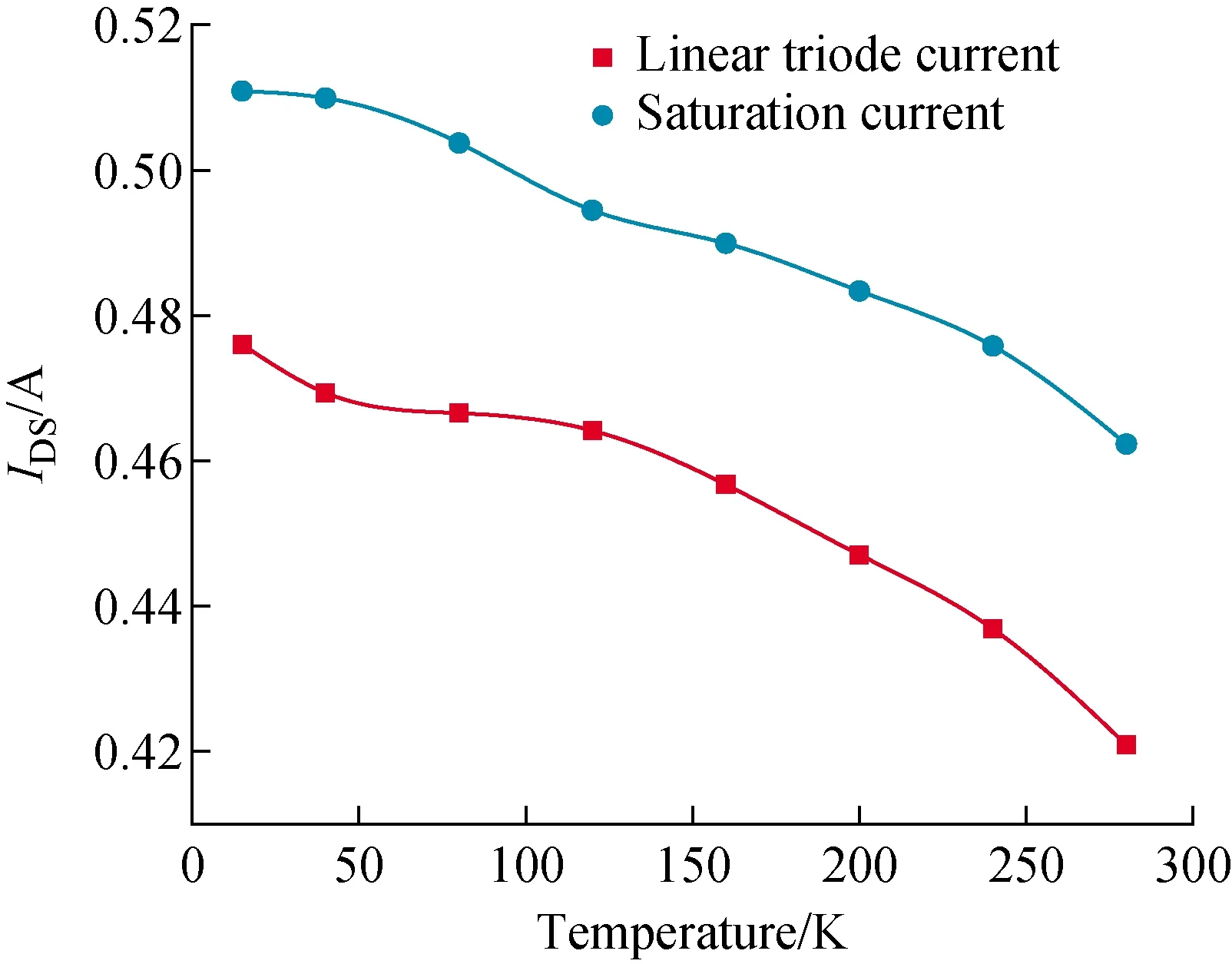
Fig.5 Linear triode and saturation regions of GaN-based MOSFET under different temperatures
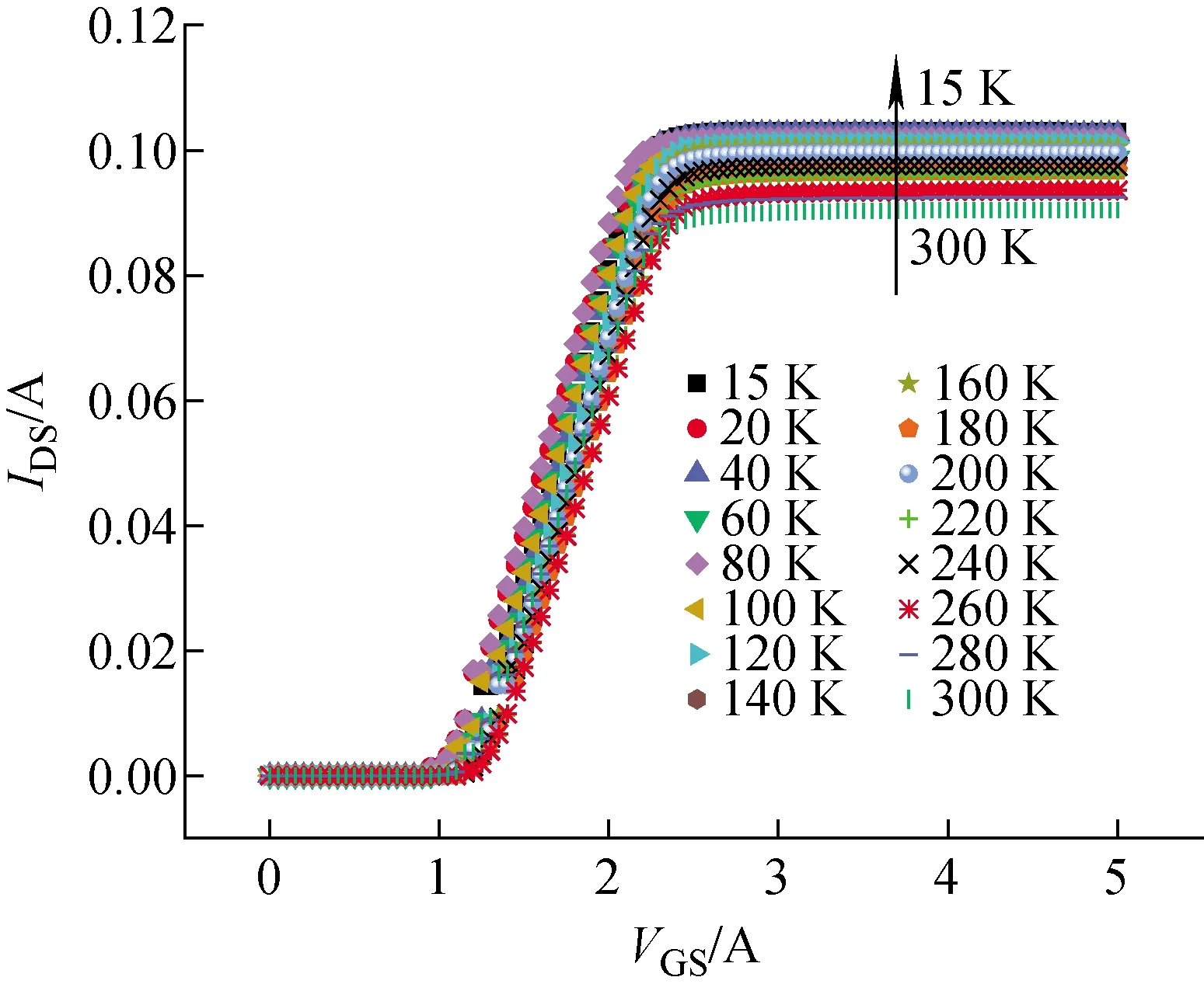
Fig.6 Transfer curves of IDS-VGS of GaN-based MOSFET for several temperatures
Threshold voltageVthfor several temperatures is shown in Fig.7. Significant increase in threshold voltage with temperature decrease is typical for GaN-based MOSFET and has been observed in both implanted DMOSFETs. This temperature dependence is explained by the high density of acceptor-like states near the conduction band edge. At relatively high temperatures, the possibility of negative charge of electrons captured by interface trap drops, the negative charge on interface decreases, and the threshold voltage decreases accordingly[14-15]. As a result, increased threshold voltage proves higher switching rate.
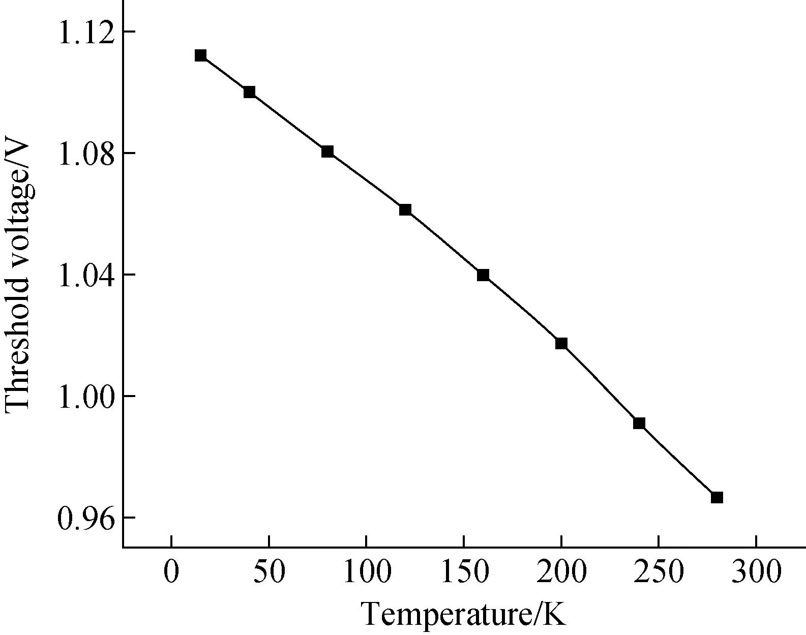
Fig.7 Threshold voltages of GaN-based MOSFET under different temperatures
From the analysis of Fig.6 and Fig.7, it can be found that the cryogenic temperature environment can also improve the transfer characteristics of GaN-based MOSFET devices to some extent.
4 Conclusion
In summary, the electrical performance of GaN-based MOSFET at temperatures from 15 K to 300 K is demonstrated and analyzed. It is found that with a decrease of operation temperature, the threshold voltage and saturated drain current increase monotonously, while the on-state resistance drops. The shift of threshold voltage of GaN-based MOSFET at cryogenic temperature is due to high interface state trappings. And the increase of saturated drain current contributes to high electronic mobility.
GaN-based MOSFET continues to function properly as temperature decrease to 15 K both on output and transfer performances and shows excellent enhanced cryogenic characteristics under the conditions of this study, indicating that GaN-based MOSFET can be capable of surviving low temperatures as cooled as 15 K.
- 原子能科学技术的其它文章
- H-1NF仿星器标准磁场位形分析与高能量离子运动轨道模拟
- 铀转化生产线含氟废水处理工艺设计
- 在线进样ICP-MS用于239Pu气溶胶活度浓度连续监测技术研究
- Degradation Characteristic of Proton Irradiated 8T CMOS Image Sensor
- Comparative Experimental Study on Space Electrostatic Discharge Effect and Single Event Effect of 130 nm SOI D Flip-flop Chains
- Effects of Electron Irradiation at Different Energy and Fluences on Electrical Properties of InP HEMT Structure

