Circuit-level Modeling and Simulation of Single Event Effects in CMOS Electronics
DING Lili, WANG Tan, ZHANG Fengqi, YANG Guoqing, CHEN Wei
(1.State key Laboratory of Intense Pulsed Radiation Simulation and Effect, Northwest Institute of Nuclear Technology, Xi’an 710024, China; 2.Xidian University, Xi’an 710071, China)
Abstract: Single event effects (SEE) induced by high energy particles can cause loss of storage data, disorder of program, and even functional error of electronic systems. Modeling and simulation of SEE has attracted much attention in recent years. Circuit-level simulation is to directly introduce radiation effects terms into the common compact model. To reach higher accuracy and more comprehensive analysis of physical mechanisms, the dependence of single event transients on strike locations was studied and analytically modeled. The principle and approach flow of the proposed circuit-level SEE simulation were presented. Firstly, basic drift and diffusion collections were considered. Secondly, bias-dependent model could be produced. Then the well potential modulation and the bipolar amplification effects were modeled. Circuit-level simulation results agree well with experiment results. Based on the performed work, transient radiation effects evaluation software (TREES) was developed. The input file should be GDSII layout, which will be parsed and all active region information will be extracted. Other user-defined options include heavy ion setup (LET values), region selection, and stimulus setup, etc. The outputs include waveforms corresponding to each strike, SEE sensitive region mapping, SEE cross section values, etc. The first edition has been integrated into commercial design flow, which can be used as a plug-in software into Cadence toolbar. The second edition is a stand-alone version with no demand for upstream or downstream commercial software. This work is useful to produce precise SEE response predictions for circuit blocks or medium-size circuits. TREES software can generate SEE sensitive region much faster than time-consuming device-level simulation. For designers who are familiar with circuit-level simulation, this approach is useful for checking the hardness performance of integrated circuits at design phase.
Key words:circuit-level; modeling and simulation; single event effects; transient radiation effects evaluation software; CMOS electronics
1 Introduction
Modeling and simulation of radiation effects is to simulate the process of radiation interaction with semiconductor electronics, through proposing physical and mathematical modeling methods, performing numerical or analytical calculation, and exporting calculation results. Multiscale approaches include particle transport simulation, device-level simulation, circuit-level simulation, etc. Among them, device-level simulation is to simulate the whole process of carrier generation, transport and collection. It can be used to explore the underlying mechanisms beneath the phenomena[1]. Comparing to this, circuit-level simulation is to directly introduce radiation effects terms into the common compact model. It could be very useful in evaluating the radiation response at design phase of CMOS electronics[2], locating sensitive circuit blocks[3], evaluating the effectiveness of hardening methods[4], identifying the worst-case bias setup during irradiation[5].
Single event effects (SEE) induced by high energy particles can cause loss of storage data, disorder of program, and even functional error of electronic systems[6]. Along with decrease in feature size of electronic devices, multiple nodes charge collections cause strong interference between adjacent transistors which the nodes belong to. This brings up new challenge for simulation technique, demanding higher accuracy and more comprehensive analysis of physical mechanisms. Modeling and simulation of SEE has attracted much attention in radiation effects community. Software including MRED from Vanderbilt University[7-8], SEMM-2 from IBM[9], MUSCA SEP3 from ONERA[10], involve Monte Carlo simulation to take into account multiple sensitive volumes and use GEANT4 codes to calculate deposited charge. The collected charges will be transformed into double-exponential current pulses and injected into related nodes. Modifications to the timing parameters are not considered. Other software including FISAR from Italy[11], TFET from IROC corporation, mainly describe the charge collection driven by electric field. These techniques use parameterization methods, assuming that only the total collected charges changed with the strike location. Kauppila, et al. demonstrated a method that parameterized the injected charges, the climbing time constant and the falling time constant based on the distance between the transistor to be studied and the strike location[2]. The model is parameterized using the 1-D distance between the strike location and the gate/drain overlapped line. Contributions from the shape and area of the drain contact are ignored.
This paper is organized as follows. Section 2 presents the modeling and simulation procedure of SEE. Section 3 presents validation results and discussion. Section 4 talks about the development of transient radiation effects evaluation software (TREES). Conclusions are drawn in Section 5.
2 Modeling and simulation of SEE
To study the influence of strike location on single event transients, 3-D TCAD structure of single nMOSFET illustrated in Fig.1a was built. From the results in Fig.1b and Fig.1c, to rebuild the current pulse for injecting into the bias-dependent single-event model, drift and diffusion collections should both be considered. The injected single-event current pulse should be the summation of pulses resulting from the two sources.
To consider the contributions from the shape and area of active regions besides only the distance from the strike location to the gate/drain overlapped line, two non-dimensional parameters are introduced including a drift factor and a diffusion factor.
The drift factor represents the percentage of excess carriers injecting directly into the drain active region. As illustrated in Fig.2a, the drift factor can be expressed by the following equation.
(1)
Where (x0,y0) represents the strike location,

Point #1 represents centre point of reversely biased nMOSFET drain contact, LET=10 MeV·cm2/mgFig.1 Drain collected current pulse when striking at various locations[12]

Fig.2 Principle of calculating drift factor value (a) and diffusion factor value (b)[12]
(xi,yj) represents centre of the selected discretized active region, andR0represents the characteristic radius in TCAD heavy ion model.
For strike locations where the charge cloud evidently overlaps with the drain active region, total collected charge and the falling time constant show very good linear dependency on drift factor values. The diffusion factor is the weighted summation based on exp(-d2/4Dt) and percentage of the excess carrier density,Dis ~18 cm2/s andtis ~3×10⁻¹⁰s[13], the diffusion factor can be expressed by the following equation.
Diffusion_factor=
(2)
Where (x0,y0) represents the strike location, (xi,yj) represents centre of theAthdiscretized region around the strike location, (xk,yl) represents centre of theBthdiscretized active region, andR0represents the characteristic radius in TCAD heavy ion model.
For strike locations away from the drain active region (no overlap), total collected charge is dependent on diffusion factor values, but with evident disturbance, due to the charge collection between the N-well and P-well contacts.
Fig.3 illustrates the principle of the proposed approach. Firstly basic drift and diffusion collections are considered. Gsd is described as the combination of two double-exponential current sources. After injecting Gsd into the Verilog-A described sub-circuit (Fig.3a), the bias-dependent model Gbd can be produced. As illustrated in Fig.3b, Gbd is placed between the drain contact and the body contact which is connected with well contacts through a resistor net and a current source between well contacts (Gwell), to model the well potential modulation and the bipolar amplification effects[14].

Fig.3 Principle of proposed approach
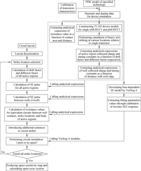
Fig.4 illustrates the approach flow of the proposed circuit-level SEE simulation. The inputs include PDK model of specified technology and layout of the circuit to be studied. The output contain the SEE sensitivity map, cross section values, etc.
3 Validation result and discussion
Fig.5 illustrates the validation results of simulated and experimental upset cross section of 40 nm DFF, where the experimental data are referring to publications[15-16]. Besides the cross section data measured atVdd=0.7 V, there are also one measured point atVdd=1.1 V and one atVdd=0.9 V, where LET=2.19 MeV·cm2/mg. It can be seen that the upset cross section gets larger at lower supply voltages, and the simulation results agree with the experimental data at various LET values and supply voltages. In general, the circuit-level simulation methodology proposed in this work is able to predict the upsets quantitatively as well.
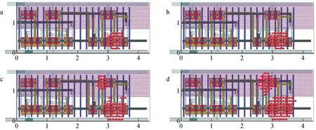
Fig.6 illustrates the sensitive region maps produced by circuit-level simulation, which help us to learn more details. The red dots suggest upset occurs when striking at the corresponding region. From Fig.6a and Fig.6b (LET=5 MeV·cm2/mg), sensitive regions get larger atVdd=0.7 V thanVdd=1.1 V.

Fig.4 Approach flow of proposed circuit-level SEE simulation[12]
Since the LET value is quite small, only a part of P-well region can be identified as sensitive regions. Then at larger LET values, sensitive region area keep increasing, covering not only P-well region, but also a part of N-well region.
4 Development of TREES
Based on the performed work, TREES was developed by our group. The first edition

Fig.5 Validation results of simulated and experimental upset cross section of 40 nm DFF, where experimental data are referring to [15] and [16]

a—LET=5 MeV·cm2/mg and Vdd=1.1 V;b—LET=5 MeV·cm2/mg and Vdd=0.7 V; c—LET=10 MeV·cm2/mg and Vdd=0.7 V;d—LET=30 MeV·cm2/mg and Vdd=0.7 V The red dots suggest upset occurs when striking at the corresponding region.Fig.6 Sensitive region map produced by circuit-level simulation
has been integrated into commercial design flow, which can be used as a plug-in software into Cadence toolbar. The input file should be GDSII layout, which will be parsed and all active region information will be extracted. Other user-defined options include heavy ion setup (LET values), region selection, and stimulus setup, etc. The outputs include waveforms corresponding to each strike, SEE sensitive region mapping, SEE cross section values, etc. The second edition is as illustrated in Fig.7, which is a stand-alone version with no demand for upstream or downstream commercial software.

Fig.7 Interface of TREES 2.0 software
TREES software can generate SEE sensitive region much faster than time-consuming device-level simulation.Fig.8 presents a group of results corresponding to NOR cell with minimum drive strength at various stimulus setups (two input terminals A and B connected with 00, 01, 10, and 11 correspondingly).
5 Conclusion
The dependence of single event transients on strike locations was studied and analytically modeled. The principle and approach flow of the proposed circuit-level SEE simulation were presented. Firstly basic drift and diffusion collections are considered. Secondly, bias-dependent model can be produced. Then the well potential modulation and the bipolar amplification effects are modeled. Circuit-level simulation results agree well with experiment results. Based on the performed work, TREES software was developed by our group. The input file should be GDSII layout, which will be parsed and all active region information will be extracted. Other user-defined options include heavy ion setup (LET values), region selection, and stimulus setup, etc. The outputs include waveforms corresponding to each strike, SEE sensitive region mapping, SEE cross section values, etc. The first edition has been integrated into commercial design flow,which can be used as a plug-in software into Cadence toolbar. The second edition is a stand-alone version with no demand for upstream or downstream commercial software. This work is useful to produce precise SEE response predictions for circuit blocks or medium-size circuits. For integrated circuit designers who are familiar with circuit-level simulation, this approach is useful for checking the hardness performance of integrated circuits at design phase.

Fig.8 SEE sensitive region for 1×NOR (NOR cell with minimum drive strength) at various stimulus setups
- 原子能科学技术的其它文章
- H-1NF仿星器标准磁场位形分析与高能量离子运动轨道模拟
- 铀转化生产线含氟废水处理工艺设计
- 在线进样ICP-MS用于239Pu气溶胶活度浓度连续监测技术研究
- Degradation Characteristic of Proton Irradiated 8T CMOS Image Sensor
- Comparative Experimental Study on Space Electrostatic Discharge Effect and Single Event Effect of 130 nm SOI D Flip-flop Chains
- Effects of Electron Irradiation at Different Energy and Fluences on Electrical Properties of InP HEMT Structure

