
Semiconductor OpticalAmplifier and Gain Chip Used in Wavelength Tunable Lasers
2021-10-26 08:36:32SATOKenjiZHANGXiaobo
ZTE Communications 2021年3期
SATO Kenji,ZHANG Xiaobo
(1.ZTE Photonics,Nanjing 210000,China;2.Southeast University,Nanjing 211189,China)
Abstract:The design concept of semiconductor optical amplifier(SOA)and gain chip used in wavelength tunable lasers(TL)is discussed in this paper.The design concept is similar to that of a conventional SOA or a laser;however,there are a few different points.An SOA in front of the tunable laser should be polarization dependent and has low optical confinement factor.To obtain wide gain bandwidth at the threshold current,the gain chip used in the tunable laser cavity should be something between SOA and fixed-wavelength laser design,while the fixed-wavelength laser has high optical confinement factor.Detailed discussion is given with basic equations and some simulation results on saturation power of the SOA and gain bandwidth of gain chip are shown.
Keywords:external cavity;gain chip;saturation power;semiconductor optical amplifier;tunable laser
1 Introduction
A wavelength tunable laser(TL)is one of the most popular light sources in digital coherent optical fiber telecommunication systems,because the use of TL can reduce the required number of inventory lasers,thereby reducing inventory cost[1].A wavelength channel can be selected on ITU grid channels,but it must be very accurate.In early days,many kinds of tuning mechanisms were proposed,but recently there exist only a few kinds of integrable tunable laser assembly(ITLA)products in the market,because it is very difficult to achieve such performance as high output power and wavelength accuracy and low cost.The modulation format used in those coherent systems is an advanced one,such as Dual Polarization Quadrature Phase Shift Keying(DP-QPSK),16 Quadrature Amplitude Modulation(16QAM),and other multilevel formats[2–3].Because the insertion loss of these advanced modulators may be large,higher optical output power of ITLA is strongly required.In addition,for the use in small form-factor pluggable optical modules like C Form-factor Pluggable 2(CFP2),Octal Small Form-factor Pluggable(OSFP),or Quad Small Form-factor Pluggable(QSFP),a part of light power is split to a coherent receiver for a light as a local oscillator due to the small package.Therefore,the ITLA with an optical amplifier in front of a laser unit has been recently becoming more and more popular.This kind of semiconductor optical amplifier(SOA)has some interesting features,such as polarization dependent gain and high saturation power.Its design can be similar to the design of a conventional laser and the SOA is sometimes monolithically integrated with a tunable laser[4].
Moreover,a gain chip is the other important topic in this paper.A gain chip is used in external cavity(EC)tunable laser configuration,and it works as a laser.Equivalently,this can be treated as a Fabry-Perot(FP)laser with a wavelength bandpass filter.Because this is a tunable laser,the gain bandwidth of the gain chip should be very wide and cover the whole Cband[5–7].Therefore,the design of the gain chip is not exactly the same as a laser,but it is not the same as that of SOA.The design concept of the gain chip is also discussed in this paper.Moreover,the gain bandwidth of Erbium-doped fiber amplifier(EDFA)is being extended over the conventional band[8–9].In the near future,a wider tuning range of tunable lasers will also be required than the conventional one.
The purpose here is to write a tutorial paper on design concept with basic equations and detailed discussion for the SOA and gain chip that are used for wavelength tunable lasers.To the best of our knowledge,the paper on such a topic has not yet existed.In Section 2,the design concepts of these two devices are discussed.The difference from conventional design is shown.In Section 3,details of tunable lasers with SOA or gain chip are explained.In Section 4,some simulation results and comparison of design concepts are discussed.Finally,conclusions are given in Section 5.
2 Design Concepts of SOA and Gain Chip
The structure of SOA is actually very important.The design concepts are basically based on a conventional SOA or a laser,which are slightly different.
2.1 SOA Design Concept
The design concept of SOA for tunable laser is similar to an inline SOA,except polarization dependence[10–11].Inline SOAs are widely used in network systems.Here it is briefly explained.SOA is used for a one-pass gain medium,so it is reasonable to define the gainG sin single-pass of SOA as

whereΓis the optical confinement factor,gis the gain in unit length,αiis the internal optical loss,andLis the length of SOA.
2.1.1 Residual Reflection
The gaingis assumed as a function of carrier density(see Section 2.1.2).As the injection current increases,the carrier densityNis also increasing.The facet reflectivity is normally very low on antireflection(AR)coatings,but in reality,residual reflection exists.The reflectivity is,whereR1andR2are front and rear facet reflectivities,respectively.Considering the round-trip gain,the laser oscillation condition is(G s R)2=1.Because the gain cannot be increased due to lasing,Rshould be as low as possible to obtain higher gain.This is the reason why both facets of SOA are AR-coated with angled waveguides.Recently,the facet reflectivity has reached lower than 10-4,which is required to operate SOA properly.The influence of residual reflection may cause the gain ripple,which is a small dependence of gain on wavelength.This is also known as a cause of noise figure.If the residual reflectivity is lower than 10-4,G swould be 40 dB.In a practical use for amplification of tunable laser output power,the small signal non-saturated gain will be around 20 dB,for instance.In this case,the gain ripple and noise are negligible for the use in tunable laser source.According to Ref.[12],the gain ripple depthmcan be described as
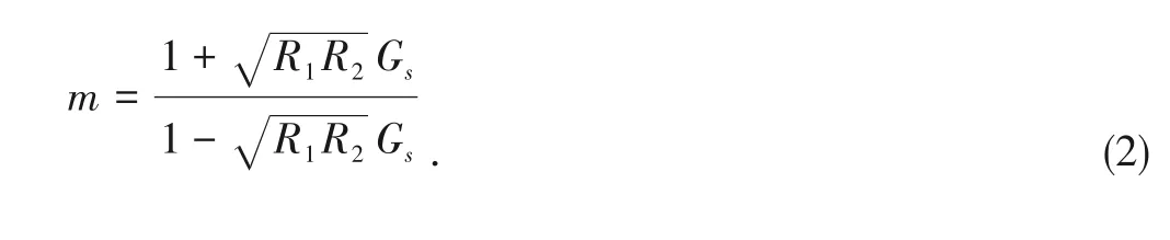
According to Eq.(2),the depthmis a function of facet reflectivity and single-pass gainG s.For example,mis 0.09 dB withR1andR2of 10-4andG sof 20 dB.To achieve such a low reflectivity,angled waveguides on both coated facets should be applied[13].Larger than 7-degree angle is sufficient to reduce facet reflectivity.
2.1.2 Saturation Power
To design SOA,it is useful to understand the following carrier rate equation[14]:

whereJis the injection current density,qis the elementary electric charge,dis the thickness of active layer,Nis the carrier density,N0is the transparent carrier density of gain medium,τSis the carrier relaxation time,Ais the differential gain,h is the Planck’s constant,andνis the frequency of light.
The intensity of lightP(W/cm2)can be described by the following propagation equation:

Here to make the phenomena simplified,the gain is proportional to the carrier density at the bulk active layer.The steady solution fordN/dt=0 from Eq.(3)can be substituted in Eq.(4),and thendP/dzcan be derived as

wherePSis the saturation intensity,described asP S=hν/τS A,andg0is a non-saturated gain coefficient,which is described asg0=-N0).When the intensity of lightPis much smaller thanPS,the gain coefficient will be nearly equal tog0.As the intensity is becoming larger,the gain coefficient will be getting smaller,obeying the term 1/(1+P/P S).To avoid such saturation of gain,PSmust be enlarged in the design.As the light is amplified in SOA,the carrier density will be consumed for stimulated emission,especially near the end.Therefore,the number of carriers will not be enough to amplify it any more.To avoid the saturation,τSorAshould be small as seen in the description ofPS.However,it is difficult to controlτSandAin reality.
In an ideal model of SOA,the output power of SOA can be described with only non-saturated small signal gain,by integratingd P/dzin Eq.(5):
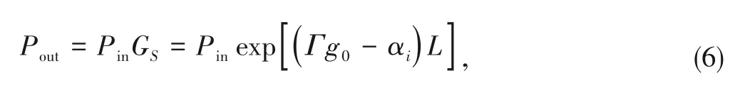
wherePoutis the output signal power,Pinis the input signal power,andLis the SOA cavity length.As seen in Eq.(6),the single-pass small signal gain is dependent onΓg0L.As the carrier density is increased,g0becomes larger and will reach saturation.However,saturation will be suppressed for the small optical confinement factorΓor short cavity lengthLwhile keeping the gainGS.This means the carrier density can be increased and then the saturation power will become larger.The saturation power[15]is described as

whereWis an active region width,dis the thickness,andEis photon energy as a function of wavelengthλ.As shown in Eq.(7),the saturation power is inversely proportional to the optical confinement factor.One simulation result on gain saturation as a function of optical confinement factor is shown in Fig.1,whereWis 2μm,dis 0.1μm,λis 1.55μm and the product ofτs Ais 6.04×10⁻²⁶s‧cm2.As the confinement factor decreases,the saturation power will become larger.
2.1.3 Polarization Issue
Low residual reflection on facet and high saturation power have been discussed above.Because this kind of SOA is used just in front of the tunable laser,some other features are also required.We focus on polarization dependence here,rather than wide gain bandwidth that is very natural to be obtained by injecting high current to the SOA.
A very common structure of an active layer contains a multiquantum well(MQW).This is a quantum well with multiple very thin layers,so the electrons’energy level to vertical direction can be quantized and then the gain has direction dependence to the quantum well structure.There exist heavy and light holes in the quantum well.The heavy holes can generate only Transverse Electric(TE)mode polarization,while the light holes can generate both TE and Transverse Magnetic(TM)mode polarizations.The inline SOA is normally required to obtain gain both for TE and TM modes as polarization independence[16–17];however,the SOA used just in front of tunable laser should have gain only for TE mode polarization.To enhance transition from the electron to the heavy hole band,a compressively strained quantum well is used here.This can be very similar to the active layer of gain chip,but it is easier to monolithically integrate the SOA on the tunable laser.Because the injection current density for SOA is very different from that for the gain chip and the optical confinement factor of SOA should be low for high saturation power,the active layer should be different rigorously.Therefore,the active layers should be different from each other,so the chips should be integrated hybridly.

▲Figure 1.Calculated saturation power as a function of optical confinement factor
2.2 Gain Chip Design Concept
The MQW as an active layer is the most common gain medium for the SOA or laser.It is good to know how to design quantum wells with a quantum mechanics theory.Only a rough image of gain design with basic parameters is introduced in this paper.Gain per length is a function of the current density of the active layer,so it can be described as:
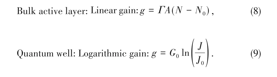
A linear gain function can be applied for the bulk active layer.On the other hand,due to a quantum well characteristic,the equation should be physically a logarithmic function of the current density[18].However,it is a function of the current density and derived from an experience law.It is widely used because it can fit the characteristic very well.Laser designers are interested in the parametersG0andJ0.G0is an indicator kind of differential gain and the optical confinement factorΓis already included.J0physically means a transparent current density.
For the waveguide quality,popular parameters used widely areαiandηi.αiis an internal loss per length andηiis a quantum internal efficiency.Forαi,it comes from an absorption of light and light scattering in waveguide and its design issue is to reduce internal loss in the waveguide.Besides,ηimeans a rate of photon generation to one carrier seed.This value is very close to 1.0 because of a good quality of quantum well media,but it is decreased due to current leakage and a lost carrier for non-radiative recombination.
To reach the laser threshold,we must have
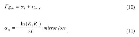
That is,the total of internal and mirror loss should be compensated by gain.Here the mirror loss is an out-going light per length in the gain region.In Eq.(10),all parameters are defined for a unit length.The cavity length is also an important parameter.The external cavity laser can be handled as an equivalent FP laser,as shown in Fig.2.The equivalent rear reflectivityR2includes the coupling loss between the gain chip and external cavity,propagation loss in external waveguide,and reflection at the end of external waveguide.
The threshold currentIthcan be varied as a function of cavity lengthL,as shown in Fig.3,whereΓis 5%,G0is 350 cm-1,αiis 8 cm-1,andJ0is 9.5×10⁴A·cm-2.It is well known that there is an optimum cavity length for the minimum threshold current.In Fig.3,the ordinal FP-laser with 30/30%facet reflectivity shows the minimum threshold current at length around 0.5 mm.On the other hand,the 5/5%FP-laser which is equivalent to external cavity tunable laser shows the minimum at 1.5 mm.The effective reflectivity from the external cavity is assumed to be around 5%,and the confinement factor of the 5/5%FP-laser has two thirds of that of the 30/30%FP-laser to have higher threshold carrier density.This also implies that the designed effective reflectivity of the external cavity should be carefully considered.An example of the external cavity tunable laser can be found in Ref.[19].
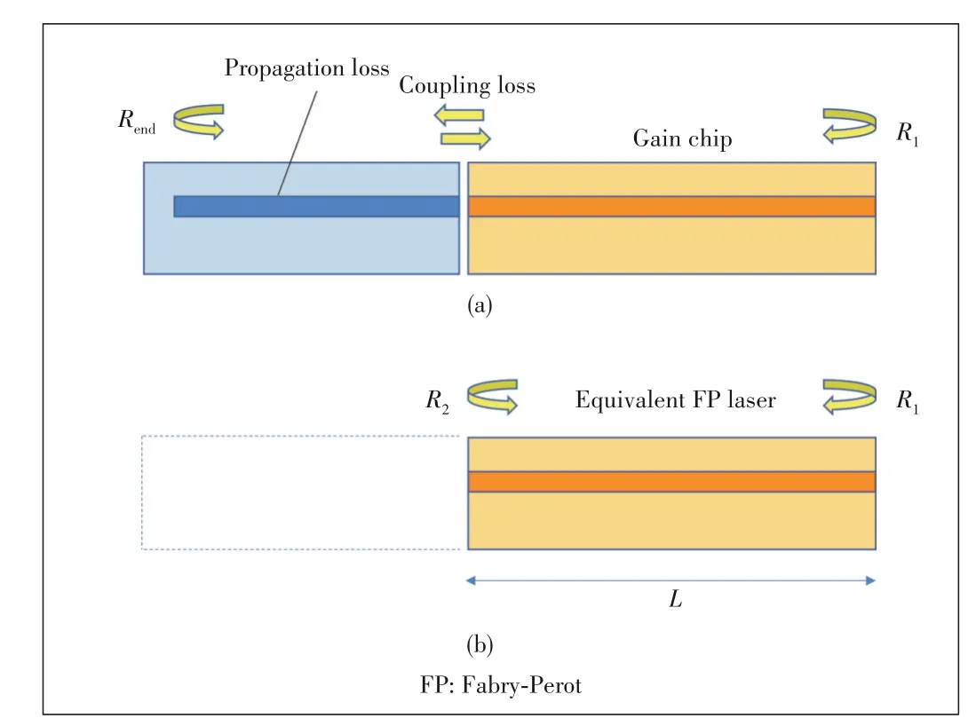
▲Figure 2.Schematic block diagram of(a)external cavity laser and(b)equivalent FP laser to external cavity with R1 and R2 with cavity length of L

▲Figure 3.Calculated threshold current as a function of cavity length with R1/R2 of 30/30%and 5/5%reflectivities
Then the output power can be described as

Therefore,the power is proportional to the current minus threshold current.If the gain is higher than the threshold gain,the light output will continue to increase and carrier density must clamp at its threshold value.That is,the energy goes to light output from the excess energy over threshold current.The carrier density cannot go higher in laser operation.On the other hand,the carrier density in SOA can go higher,due to a very high threshold current with smallR1andR2.This is the biggest difference between the SOA and the laser design.It is generally said that the design principle of SOA is opposite to the laser design.An SOA needs a lot of carriers to amplify the light in one direction and should avoid the carrier depletion in the cavity.
The gain bandwidth is also an important specification in gain chip.To realize very wide gain bandwidth,the carrier density at the threshold should be larger than that of an ordinary laser,but it should not be too high.The reflectivity of the cavity is rather low,like 5%,so naturally the threshold density increases;however,it is not enough.To tune the carrier density,it is good to take a smaller number of quantum wells or low optical confinement factor at the active layer,compared with an ordinary laser.
2.3 Summary
The gain chip design concept is to obtain wide gain bandwidth with low optical confinement factor and low residual reflectivity at the facet on the tunable filter side.The SOA design concept is to achieve high threshold current with low residual reflectivity and low optical confinement factor.
3 Examples of Tunable Lasers with SOA
Some examples of tunable lasers with the gain chip and SOA are shown in this section.Generally,there are three major categories of tunable laser configuration with SOA,as shown in Fig.4.
The first type is the arrayed distributed feedback(DFB)laser with integrated SOA[20–23].This type has a long history of development.In early days of this research,the number of DFB lasers were limited,and the optical coupler was an multimode interference(MMI)coupler with SOA or Micro Electro Mechanical Systems(MEMS)coupler without SOA[24].In the case of MMI couplers,the optical loss is large and then the SOA is needed.This type with SOA is suitable for monolithic integration and its wavelength tuning mechanism is simple to tune only temperature of the chip.For monolithic integration,waveguides of active and passive regions are separately grown by Butt-joint technology.The same active layer is utilized both for laser and SOA regions.This means the freedom of SOA design is slightly limited.
The second type is the distributed Bragg reflector(DBR)tunable laser with a Vernier effect of two grating regions,implemented by multiple methods,such as sampled grating[25],digitally sampled(DS)DBR[26],and chirped sampled grating[27].In this paper,the sampled grating is not the subject,so it is not discussed.Because the reflectivity of DBR must be rather high,the output power directly from the DBR tunable laser will be not high enough.Therefore,an SOA after the DBR laser is usually needed.In the same manner as the DFB arrayed type,the SOA in the other two types can be monolithically integrated by Butt-joint or Ion-implantation technology[28]on the same chip as a tunable laser part.The same active layer is also utilized.
The third one is an external cavity tunable laser with a gain chip[5,18,29].The tunable laser is configured with an external tunable bandpass filter with a reflector and a gain chip.This gain chip can be handled as a FP-laser with a front facet mirror and a rear effective mirror of external filter,as mentioned above.In the case of silicon tunable filters,the gain chip and the filter chip are hybridly integrated.Because it is also difficult to obtain high output power directly from the gain chip,the SOA is also hybridly integrated to amplify the optical power.The gain chip and SOA cannot be monolithically integrated due to the facet reflectivity of the gain chip.Therefore,the freedom of SOA design is not limited to have high saturation power with lower optical confinement factor.One drawback is difficult optical coupling between chips,such as the interface of the filter and gain chip,and the gain chip and SOA.An advanced mounting technology is necessary for realizing low coupling loss.
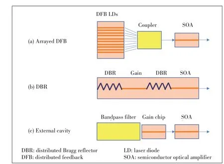
▲Figure 4.Tunable lasers with semiconductor optical amplifier(SOA)
4 Simulation Examples and Discussion
In this section,the issue on optical confinement factor is discussed.Fig.5 shows an example of measured optical signal gain as a function of amplified output power.As output power increases,the signal gain is becoming saturated.The point where the gain is decreased by 3 dB is called the saturation gain.As the injection current increases,the maximum output power will also increase,but it is also saturated even if the injection current keeps increasing.
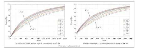
In order to investigate saturation,internal power distribution in the SOA along the cavity axis with various optical confinement factors is calculated(Fig.6).In this simulation,the SOA cavity is divided into small sections where the gain is saturated and slightly different from each other.The saturated gain in thei-th section can be described asg i=g/(1+εP),which depends on powerPand saturation coefficientε,whereεis 1/Psand saturation powerPsis 22 dBm.Those parameters of confinement factors in Fig.6 mean relative confinement factorΓr,where the actual confinement factor is a product of variableΓrand fixedΓ0of about 4%or so in reality.As shown in Fig.6,a low relative confinement factor shows more linear amplification along the cavity than high confinement.In the case of amplification for the tunable laser,the input power to SOA is high,so it cannot be treated as a small signal.When an output power higher than 20 dBm is required,the light is amplified in almost saturation region with an amplification factor of around 10 dB for the input power of 10 dBm,as shown in Fig.6(a).When the input power is 7.5 dBm in Fig.6(b),the output power is about 20 dBm.Even if the input power changes,the output power is almost constant.This implies that confinement factor should be properly designed to suppress gain saturation,otherwise the consumption power of the amplification will increase.In Fig.6,additional 1.5 dB gain is obtained to the half of the normalized optical confinement factor.

▲Figure 5.Measured optical signal gain for 1.55μm light as a function of output power from a 2 mm long semiconductor optical amplifier(SOA)
▲Figure 6.Calculated internal power distribution in SOA
Finally,the design concepts are summarized in Table 1,where the gain chip design concept can be placed between the SOA and laser design.The key parameter is the optical confinement factor.It is easy to convert the optical confinement factor into the number of quantum wells in the practical design.The active layer of the gain chip design is very similar to that of SOA except facet reflectivity,however the optical confinement factor should be slightly different from that of SOA,as mentioned above.Monolithic integration of SOA with the laser part almost works well.On the other hand,better performance should be obtained from hybrid integration with slightly different design,according to the principle.
5 Conclusions
The design concepts of the SOA and gain chip for wavelength tunable lasers are presented in this paper.The optical confinement factor of SOA should be low to realize high saturation power and be optimized only for TE mode polarization.The optical confinement factor of the gain chip should be rather lower than that of an ordinary laser and its length should be rather longer.It is also important to consider proper effective reflectivity of the external cavity to optimize performance of external cavity lasers.

▼Table 1.Comparison of design concepts

- ZTE Communications的其它文章
- ZTE Communications Guidelines for Authors
- Editorial:SpecialTopic on Wireless Intelligence for Behavior Sensing and Recognition
- Feedback-Aware Anomaly Detection Through Logs for Large-Scale Software Systems
- Super Resolution Sensing Technique for Distributed Resource Monitoring on Edge Clouds
- QoE Management for 5G New Radio
- A Survey of Intelligent Sensing Technologies in Autonomous Driving