Detection and Depth Estimation of Microdefects on Sapphire Substrate Surface
2021-09-26 09:43:38CUIChangcaiYANGChengLIZiqing
华侨大学学报(自然科学版) 2021年5期
CUI Changcai, YANG Cheng, LI Ziqing
(Institute of Manufacturing Engineering, Huaqiao University, Xiamen 361021, China)
Abstract: Using the linear-array camera scanning technology and the vertical-scanning white-light interference technology, the microdefects on sapphire substrate surfaces were located and their depths were assessed. First, the full-field scanning was carried out with linear-array camera measurement equipment to obtain full-field images of the substrate; then, the position coordinates of the microdefects were detected by extracting their centroid coordinates; finally,the three-dimensional morphology of microdefects was reconstructed to identify the type of defects,and extract the defect depth using white-light interferometry system. It takes only about 10 seconds to scan a diameter 10.16 cm sapphire substrate surface by the linear-array camera measurement system. It takes about 76 seconds to detect one microdefect by the white-light interferometry system. The deepest defect was with a depth of 7.09 μm, and a total of 13 defects (10 pits and 3 cracks or scratches) were identified and localized. The experimental results show that the proposed method can accurately locate microdefects and extract their depths on sapphire substrate surfaces.
Keywords: sapphire substrate; microdefect localization; depth estimation; linear-array camera; white-light interferometry
Sapphire substrates serve as foundations for optoelectronic product manufacturing because of their advantages including high hardness, stable chemical properties, and excellent electrical insulation[1]. It′s used in applications of national defense, aerospace systems, solar cells[2-3], chip manufac-turing, light-emitting diodes (LED)[4-6], and other fields. Since the beginning of the 21st century, the rapid developments in manufacturing technologies have increased the quality requirements for end products. In particular, higher requirements are imposed on the quality of sapphire substrate surfaces. As the substrate material of the chip, sapphire substrate will inevitably produce defects in the process of processing. Once the defects exist, there will be hidden dangers of fragments in the subsequent chip manufacturing process, which will cause huge waste. Therefore, the detection of surface micro defects is particularly important. The detection of such microdefects not only facilitates the substrate quality evaluation but also provides a basis for optimizing the substrate processing techniques. The typical substrate size increased from 2 to 8 inches (1 inch=2.54 cm), so fast and accurate detection of microdefects is very important. Microdefects can be characterized mainly by the defect depth, because a deep defect causes disastrous substrate fracture and the depth represents a useful index for subsequent processing.
Common types of microdefects on sapphire substrate surfaces include pits and cracks. In general, defect measurement and detection methods can be categorized either as destructive or non-destructive[7-8]. For destructive methods[9], the substrate samples are destroyed in the measurement process, which is also complicated and expensive. Non-destructive methods include ones based on optical interferometry[10-12], laser scattering[13-14], linear charge-coupled device (CCD) scanners[15-16], detection technology of bright-field and dark-field[17-19], scanning electron microscopy[20], scanning acoustic microscopy[21-22], laser-acoustic method[23-24]and so on. The while light interferometry and confocal scattering can detect the depth of defects, they have very high measuring accuracy, their horizontal resolution is determined by the displacement stage, which is micron level, and the axial resolution is nanometer level. If the confocal laser microscope is used to locate and measure the surface defects in the whole field, it is necessary to scan in axial direction and horizontally. For the larger sample, the efficiency is low. The white light interferometry can identify the defect position, but it is difficult to keep the interference fringe in the image at all times when scanning horizontally[25]. Besides, the field of view of traditional optical microscope is very small, so it will take a lot of time to scan the substrate surface in full field. The traditional optical microscopy methods can detect defects and extract their depths, but the defect positions on large substrates are difficult to locate. For the linear CCD scanning methods, the surface defects can be identified in large fields, but the defect depths cannot be accurately detected. The location of surface defects can be obtained by light and dark field illumination detection, but it is smaller sensitive to the depth of defects than while light interferomety. The resolution of scanning electron microscopy can reach nanometer level, but it has a high requirement for measuring environment, and the preparation of samples is complex, besides, it can not measure the depth information of defects. The scanning acoustic microscope can scan the surface of substrate in full field and locate the defects, but it can only obtain one-dimensional information of the defects in the scanning direction, and can′t restore the three-dimensional morphology. The field of view of laser acoustic method is small, so it is difficult to meet the needs of large area scanning. Compared with interferometry, the accuracy of laser acoustic method is low.
To realize fast scanning and positioning of all field microdefects on the substrate surface, and detect the depth of microdefects, we propose a measurement way that combines a linear-array camera scanner with a vertical-scanning white-light interferometer[26]. First, full-field scanning is carried out with linear-array camera measurement equipment to obtain full-field images. Secondly, a horizontal-scanning coordinate system is established by recognizing sapphire substrate boundaries, and extract the centroid coordinates of microdefects. Finally, the coordinates in this horizontal-scanning coordinate system are transformed into the coordinates of a vertical-scanning white-light interferometry system, the coordinates of microfects were obtained in white-light interferometry system, in which the type of a defect is identified based on its three-dimensional morphology. A defect-free area is used as the reference for measuring defect depths in the whole field.The experimental results show that the combination of these two measurement and detection techniques can achieve accurate microdefect localization and detection on substrate surfaces. Indeed, the proposed combined measurement method overcomes the shortcomings of each of the two individual measurement systems.
The remainder of this paper is organized as follows. Section 2 presents the working principles and the employed methods. Section 3 describes the experimental work, and the associated analysis. Section 4 concludes the paper.
1 Principles and Methods
Schematics of thelinear-array camera scanner and the vertical-scanning white-light interferometer are shown in figure 1(a) and figure 1(b), respectively.
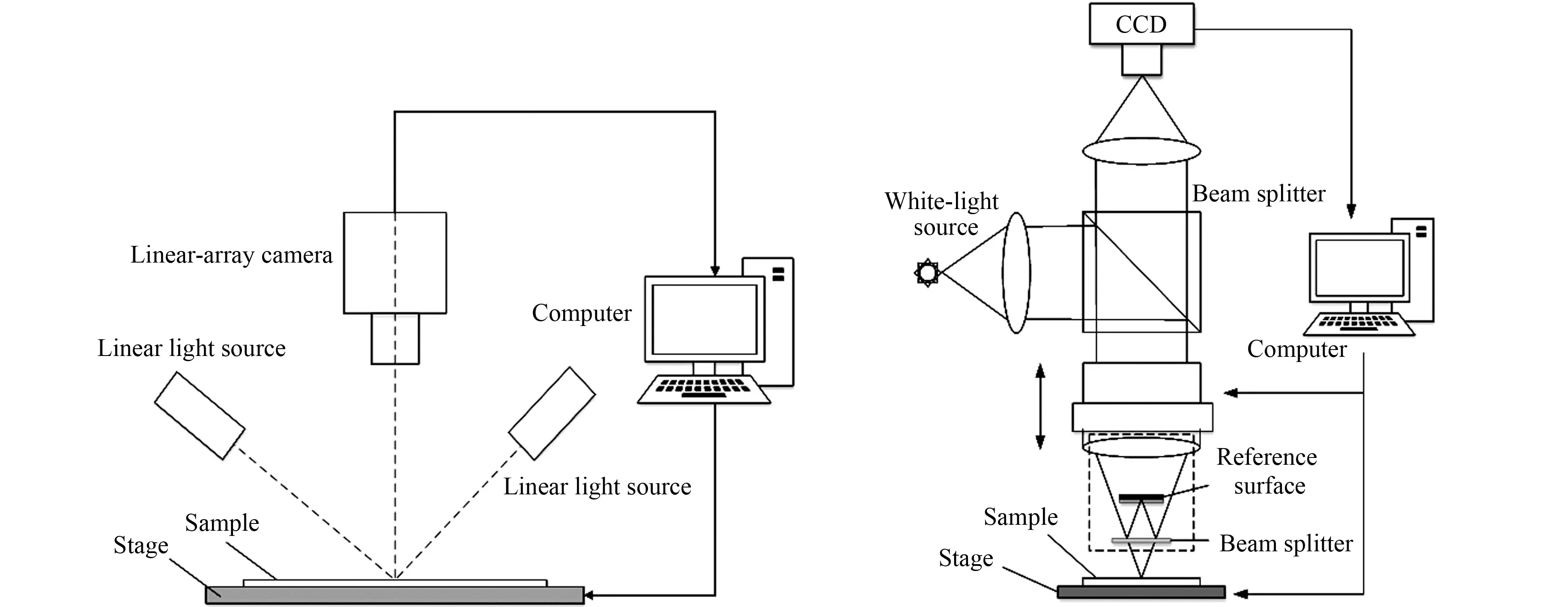
(a) Linear-array camera with substrate loss reduction (b) Schematic of vertical-scanning interferometer based on antenna-on-chip design Fig.1 Schematics of linear-array camera and interferometry measurement systems图1 线阵相机和干涉测量系统的示意图
The measurement system of a linear-array scanner consists mainly of a linear-array camera, a linear-array light source, a displacement
Table and a computer. Because of the high resolution of the linear-array camera, the measurement accuracy of this system can reach the micron level. As shown in figure 1(b), the vertical-scanning white-light interferometry system includes mainly a white-light source, a beam splitter, a CCD camera, a Mirau-type interference objective lens, a displacement stage, a piezoelectric ceramic actuator made from lead zirconate titanate (PZT), and a computer.
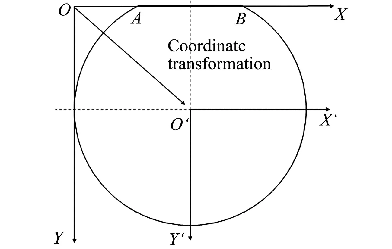
Fig.2 Establishment of coordinate systems for linear-array camera and interferometer图2 线阵相机和干涉仪 坐标系的建立
1.1 Coordinate System Setup for Linear-Array Scanner
After processing the substrate image, the defect coordinates are obtained under the scanning measurement system of the online array camera. Because the coordinate origin of the linear camera measurement system and the substrate surface are not in the same focal plane. In order to facilitate the measurement, the center of the sapphire substrate is taken as the coordinate origin of the white light interference measurement system. Therefore, if the defect is to be detected by vertical scanning, the defect coordinates need to be converted to the coordinates of white light interferometry system. The establishment of the associated coordinate system are demonstrated in figure 2.
The coordinatesXOYrepresent the coordinate system of the linear-array camera system, while the coordinatesX′O′Y′ constitute the coordinate system of the vertical-scanning white-light interferometry system. The combined measurement system works as follows. First, the linear-array camera scans the surface of the substrate quickly, and acquires a scanning image. Secondly, the boundary of the substrate is extracted by the Canny algorithm of vertical edge. TheXOYcoordinate system is established with the extension lineABtaken as theX-axis, and the tangent line perpendicular to theX-axis as theY-axis. Moreover, the defect is algorithmically detected, and the position of the defect is extracted. Finally, the position of the defect is transformed into the coordinate system of the vertical-scanning white-light interferometry system. In this paper, a 10.16 cm substrate is taken as an example. The diameter of the 10.16 cm substrate is 100 mm, and the distance betweenABand the center of the circle is 48 mm. As shown in figure 2, when the coordinate systemXOYis transformed to the coordinate systemX′O′Y′, theXandYcoordinates are reduced by 50 and 48 mm, respectively.
1.2 Defect Recognition Algorithm
The flow chart of the defect recognition algorithm is shown in figure 3.
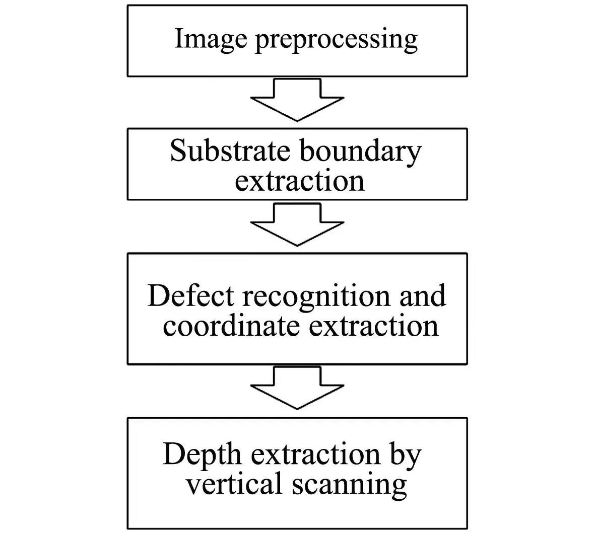
Fig.3 Flow chart of defect recognition algorithm图3 缺陷识别算法流程图
After a scanned image is obtained, pre-processing steps are applied. Because the image generated by the linear-array camera is typically very large, a region of interest (ROI) should be identified to avoid high computational costs. In particular, this ROI, which is the area where the substrate is located, can be extracted by the Canny algorithm of vertical edge. Hence, a coordinate system is established, then, the ROI is segmented by threshold, and the affected region of microdefects is extracted. So the defects within the ROI are detected and recognized, and the centroids of microdefect are extracted. After that, the center of mass coordinate of the defect needs to be converted to the coordinate system of the white light interferometry system, which is used as the basis to control the displacement
Table of the white light interferometry system to realize the defect location. Finally, the vertical scanning of the defect locations is carried out to extract the defect depths. Recognition of the defect types is then achieved by analyzing the three-dimensional morphology of each defect.
2 Experiments and Analysis
The combined measurement system used in the experiments below is shown in figure 4.The actual component models used in the linear-array camera scanning system are listed in
Table 1, while theguide rails are realized by a programmable logic controller (PLC).
The resolution ofthe linear array camera measurement system is 1 px×8 192 px, the pixel size is 3.5 μm×3.5 μm, the field of view width of the camera is 22.1 cm, and the lens focal distance is
51.2 mm, In horizontal scanning measurement, the moving speed of displacement
Table is 12 mm·s-1, and the scanning speed of camera is 4 444 Hz.
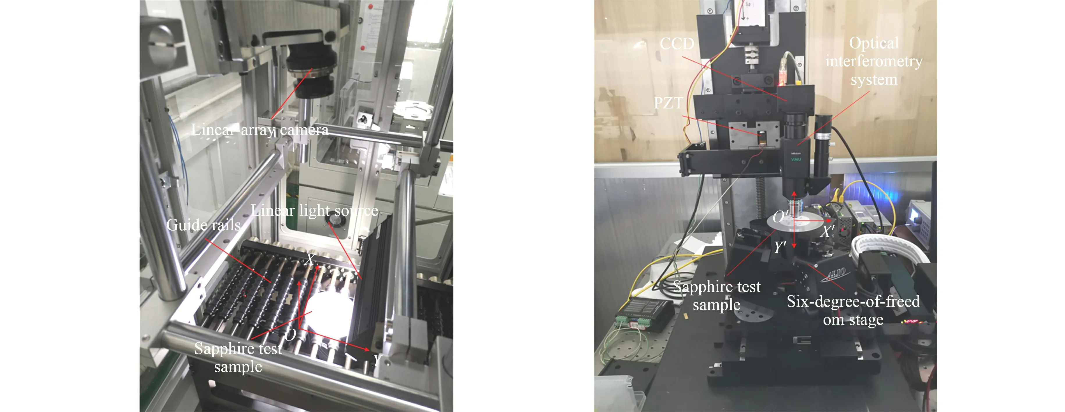
(a) Linear-array camera system (b) Vertical-scanning white-light interferometry system Fig.4 Actual images of combined measurement system图4 组合测量系统实景图
The components used in the vertical-scanning white-light interferometry system are listed in
Table 1.The resolution of the white light interferometer is 0.45 μm, the pixel size is 5.2 μm×5.2 μm, the central wavelength of the white light source is 550 nm, the field of view of the lens is 0.27 mm×0.36 mm, the depth of field is 3.6 μm, the horizontal displacement accuracy of the displacement
Table is
0.1 μm, and the velocity is 0.01 mm·s-1. The moving step distance of the piezoelectric ceramic is 40 nm when it is measured by vertical scanning.
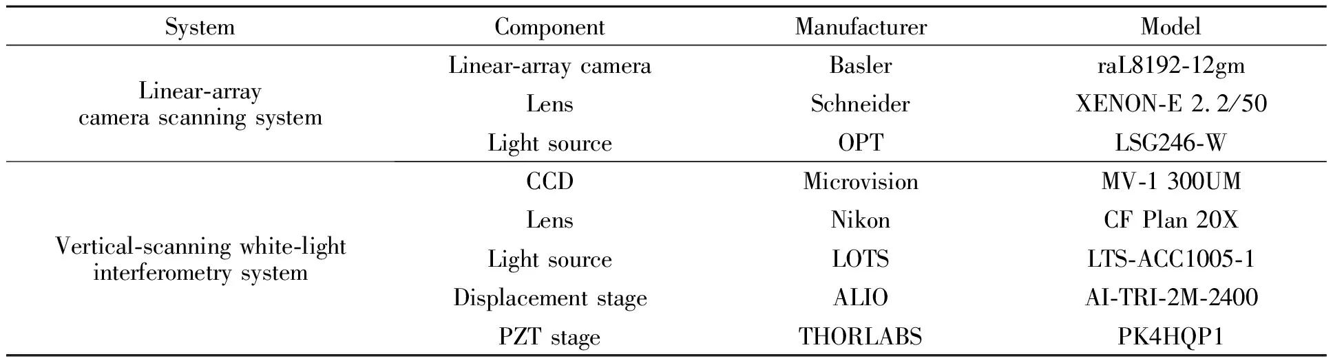
Tab.1 List of components used in linear-array camera scanning system表1 线阵相机扫描系统所用元器件一览表
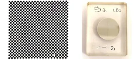
(a) Square standard pattern (b) Single-groove standard pattern Fig.5 Standard patterns for measurement system calibration图5 测量系统校准的标准件
In this work, the used measurement sample is a 10.16 cm sapphire substrate wafer, which has some deliberately-added surface defects, where the size of each defect is about one micron. The substrate thickness (d) is 0.56 mm, the surface roughness (Ra) is 0.532 nm, and the length of the corresponding sideABis 30 mm.
2.1 Measurement System Calibration
The linear-array camera measurement system and the vertical-scanning white-light interferometry system are respectively calibrated with a square standard pattern of 2-mm width and a single-groove standard pattern of 1.2-micron depth. These patterns are shown in figure 5.
For the square calibration pattern of the linear-array scanner, the values of occupied pixel are calculated with ten black-and-white squares (whose actual length is 2 cm) as a whole. Seven sets of data are collected as shown in
Table 2.

Tab.2 Experimental datasets of square calibration pattern for linear-array camera表2 线阵相机方形标定图案实验数据集
From
Table 3, it can be seen that the actual distance represented by a pixel in the linear-array camera system is about 27 μm.
For the single-grove calibration pattern of the vertical-scanning interferometry system, the groove depth isH=1.2 μm. Seven sets of data are obtained as shown in
Table 3.
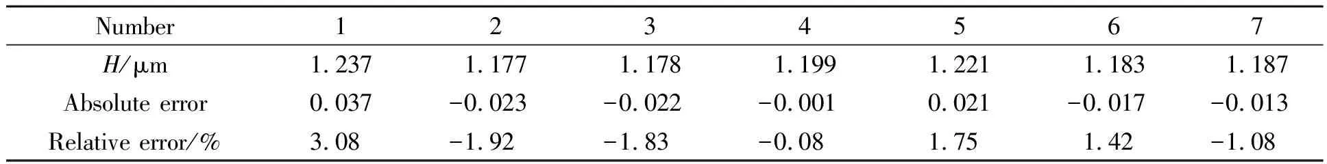
Tab.3 Experimental datasets of single-groove calibration pattern for interferometerTab.3 干涉仪单刻线标准件的实验数据集
From
Table 3, we can see that the maximum relative error of the seven datasets is 3.08%, which is within the acceptable range. Because the microdefect size in this paper is about one micron, the system measurement accuracy can meet the measurement requirements.
2.2 Microdefect Localization
The surface of the substrate sample is scanned by the linear-array camera system. Afterbinarization of the image, it is shown in figure 6.
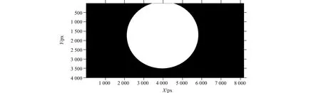
Fig.6 Substrate surface scanning outcome图6 衬底表面扫描结果
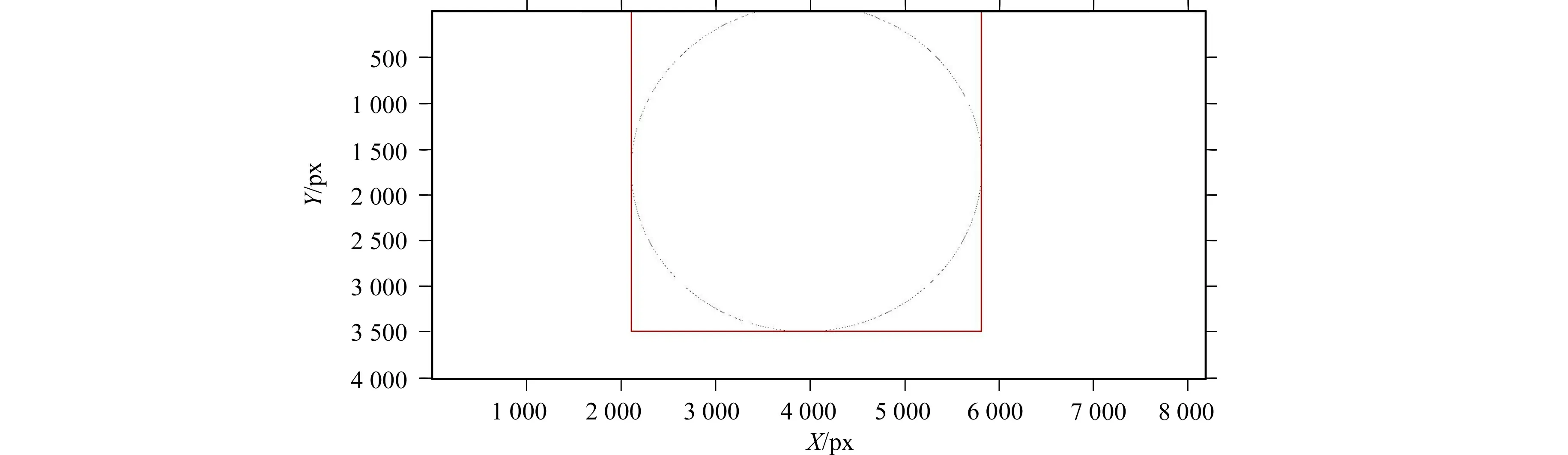
Fig.7 Image preprocessing outcome for substrate area extract Fig.7 衬底区域的图像预处理结果
The binary image is pre-processed by the Canny algorithm of vertical edge to extract the substrate area and extract ROI by rectangle box. The preprocessing outcome is shown in figure 7.
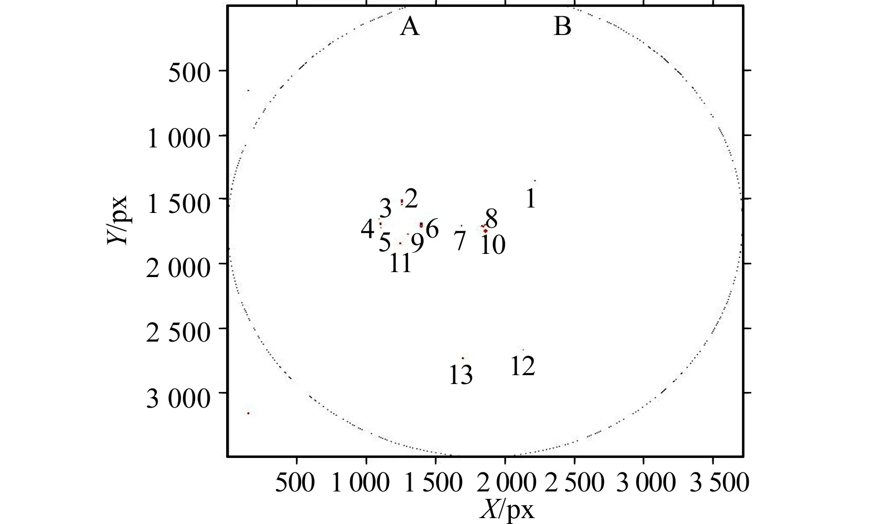
Fig.8 Locations of microdefects in test sample图8 试样中微缺陷的位置
The ROI is cut from the original image, and it′s segmented by threshold, the affected region of microdefects is extracted. So the defects within the ROI are detected and recognized, and the centroids of defect are extracted. Establish the rectangular coordinate system with the upper left corner of the image as the origin. Finally, the centroid(s) of defect are extracted as the defect coordinates.
For the given sample, the centroids of defect are shown in figure 8, where the red dots represent the identified microdefects locations. In the current experiment, 13 microdefects were identified. The number in the figure indicates the serial number of the defect.
The coordinate values are then transformed into the actual distance values combined with the scanning accuracy of the linear-array camera. We get the coordinates of each defect as shown in
Table 4. In order to facilitate the depth detection of defects, it is necessary to transform the defect coordinates into a coordinate system with the center of the substrate as the origin. Then, these values are associated with the actual input values of the displacement
Table for the vertical-scanning white-light interferometry.
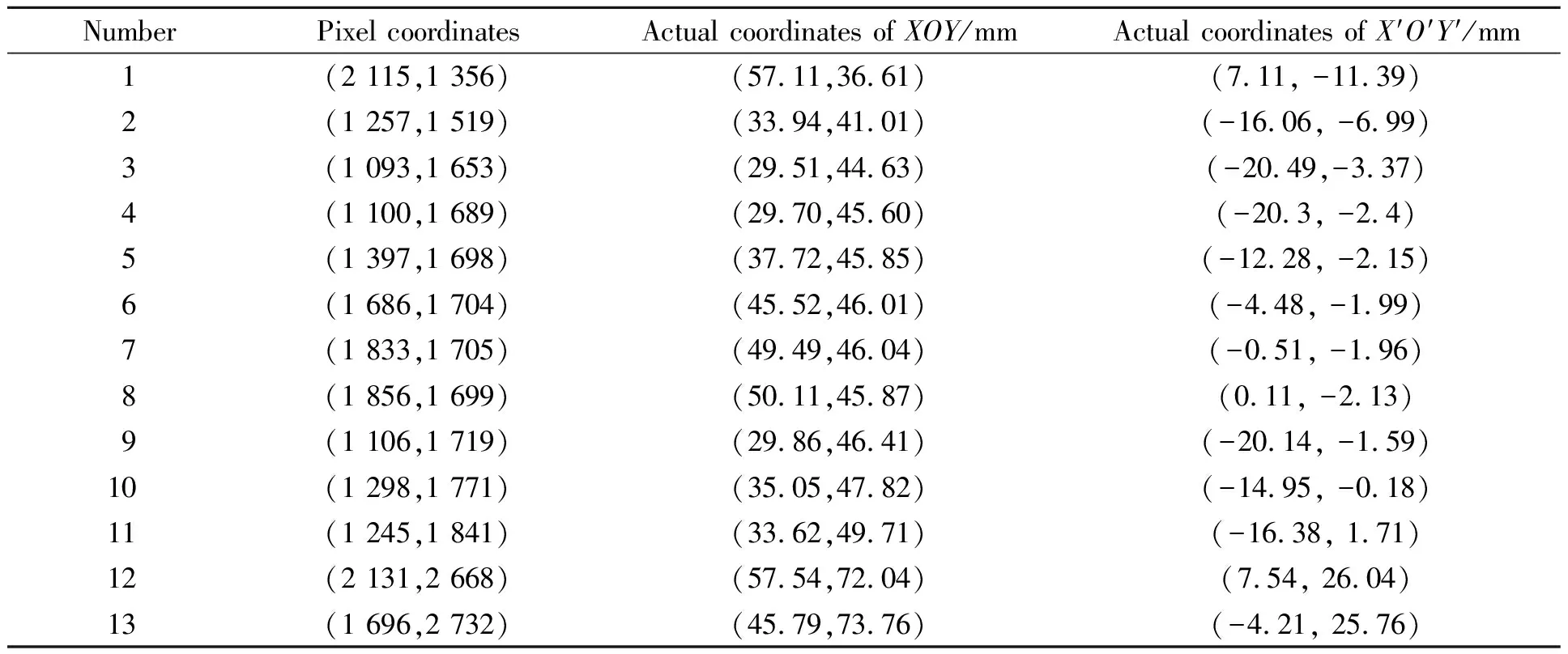
Tab.4 Defect location coordinatesTab.4 缺陷位置坐标
3.3 Depth Extraction
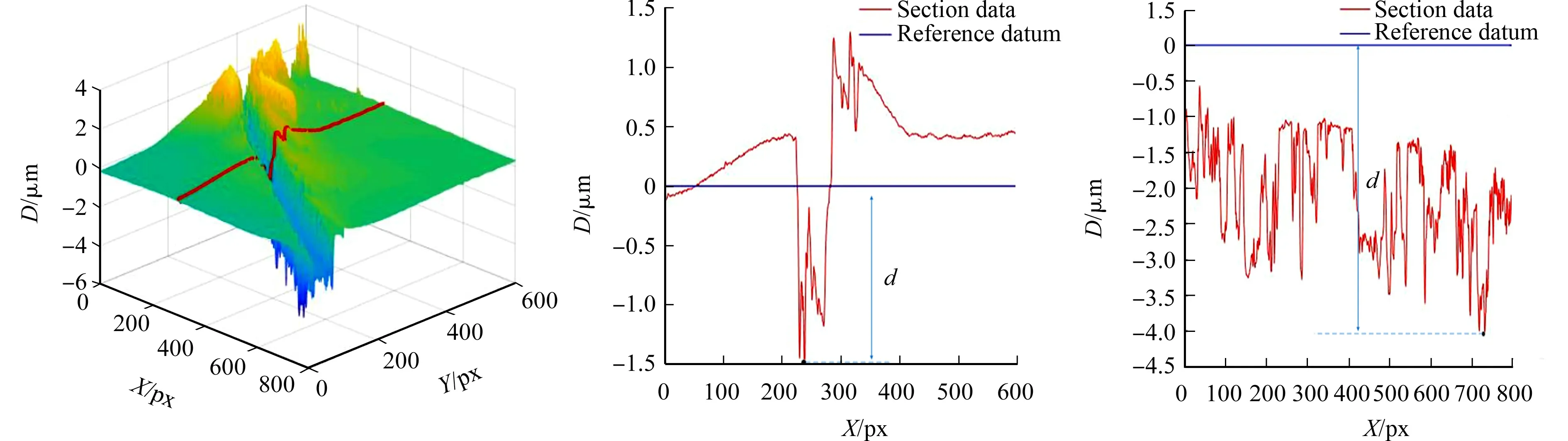
In order to better compare the depth information of different defects, we use the defect-free portion of the surface as a reference datum. This enables us to extract the defect depth information, as shown in figure 9(a). We extract the reference data from the red-box region.
For the given substrate sample, the 13 defects were scanned vertically, and the acquired topographies were reconstructed. The three-dimensional morphology surface of the tenth pit-type defect is shown in figure 10(a), while a cross-sectional view corresponding to the deepest pit position is shown in figure 10(b). The depth of the pit relative to the reference datum is 4.92 μm.
(a) Three-dimensional reconstructed pit (b) Cross-sectional pit view Fig.10 Reconstruction of 10th pit-type defect图10 第10个缺陷凹坑的形貌恢复
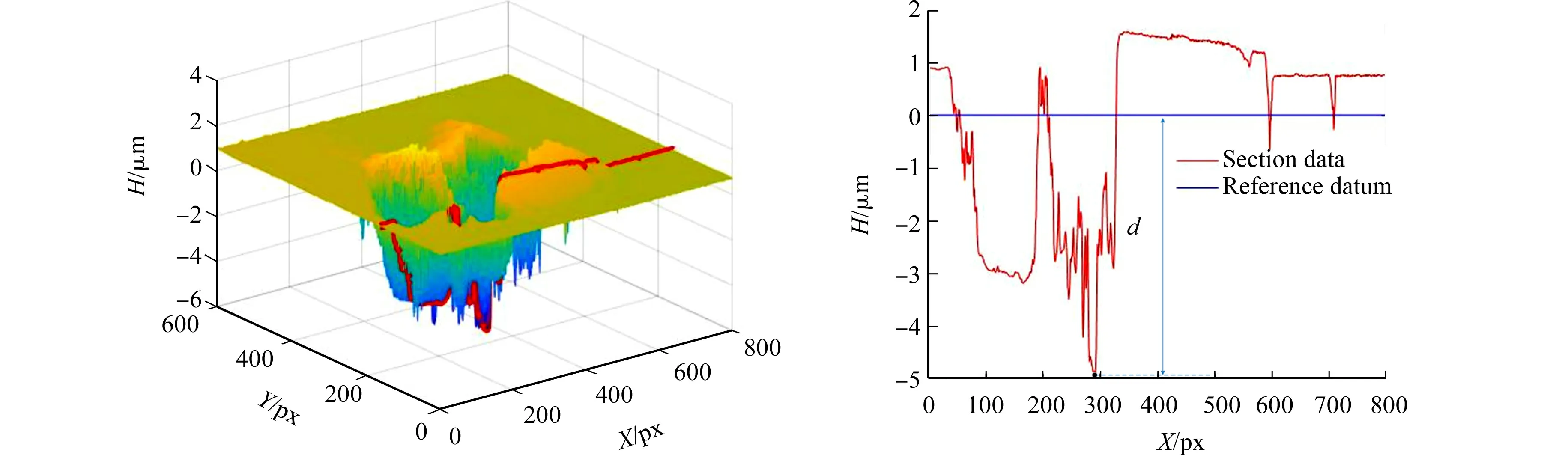
The three-dimensional morphology of the eighth crack-type defect is shown in figure 11(a), and a cross-sectional crack view corresponding toX=300 is shown in figure 11(b). In figure 11,Dis expressed as the depth value.
(a) Three-dimensional parallel to Y-axis (b) Crack profiles reconstruction of crack (c) Trend diagram of crack depth projected onX-axis (along crack valley) Fig.11 Reconstruction of 8th crack-type defect图11 第8个缺陷裂纹的形貌恢复
Tab.5 Depths of microdefects on surface of sapphire substrateTab.5 蓝宝石衬底表面微缺陷的深度
Taking theX-axis as the sampling direction, we obtain the lowest point of each section relative to the reference datum. As shown in figure 9(b), the coordinates of the 800 lowest points are projected on theX-axis direction, and the crack depth trend is obtained, as shown in figure 9(c). The crack depth relative to the reference datum was 4.04 μm.
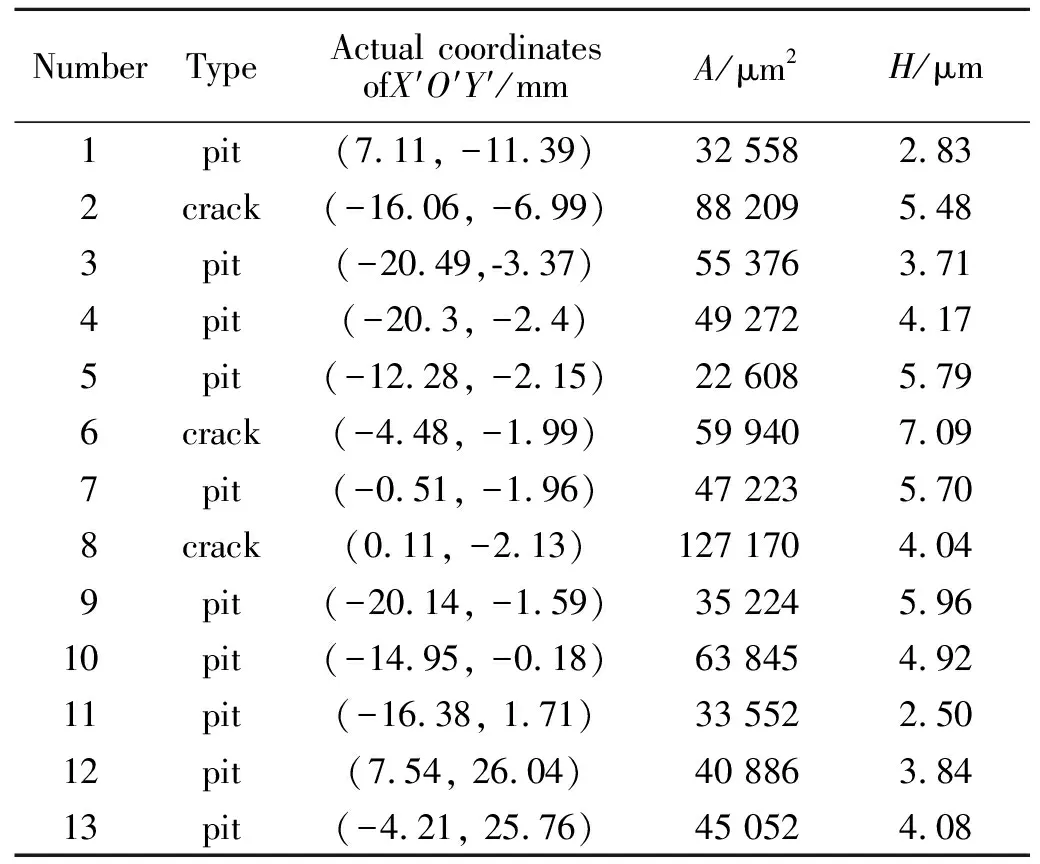
The defect coordinates are transformed and detected by the vertical-scanning white-light interferometer. The results for the 13 sample defects are shown in
Table 5. In
Table 5,Ais expressed as area.
Table 5 shows that the sixth defect is the deepest (with a depth of 7.09 μm), while the eleventh defect is the shallowest (with a depth of 2.50 μm).
4 Conclusions
Combining the linear-array camera scanning technology with the vertical-scanning white-light interference technology, we can locate and detect surface defects of sapphire substrates, reconstruct the three-dimensional defect morphology, identify the type of defects, and extract the defect depth information.
In this paper, a 10.16 cm sapphire substrate is used as the detection object. It only takes about 10 s for a 10.16 cm substrate surface to be scanned and localized by the linear-array camera measurement system. A total of 13 defects (including 10 pits and 3 scratches or cracks) were detected and identified on the substrate surface, with the deepest defect of a depth that is equal to 7.09 μm. It takes about 76s for the white-light interferometry system to detect one microdefect. Combining the two measurement methods effectively overcomes the shortcomings of a single measurement system.
猜你喜欢
新技术新工艺(2022年10期)2022-11-21 02:30:14
机械工业标准化与质量(2022年4期)2022-08-12 02:20:54
九江学院学报(自然科学版)(2022年2期)2022-07-02 02:34:06
少儿美术(2020年1期)2020-12-06 06:56:22
计测技术(2020年6期)2020-06-09 03:27:14
航天电子对抗(2019年4期)2019-06-02 08:22:40
制导与引信(2017年3期)2017-11-02 05:16:58
汽车零部件(2014年5期)2014-11-11 12:24:34
组合机床与自动化加工技术(2014年12期)2014-03-01 02:23:00
中国质量与标准导报(2014年1期)2014-02-28 22:21:34