A15 Gbps-NRZ, 30 Gbps-PAM4, 120 mA laser diode driver implemented in 0.15-μm GaAs E-mode pHEMT technology
Ahmed Wahba, Lin Cheng, and Fujiang Lin
School of Microelectronics, University of Science and Technology of China, Hefei 230026, China
Abstract: This paper presents the design and testing of a 15 Gbps non-return-to-zero (NRZ), 30 Gbps 4-level pulse amplitude modulation (PAM4) configurable laser diode driver (LDD) implemented in 0.15-μm GaAs E-mode pHEMT technology. The driver bandwidth is enhanced by utilizing cross-coupled neutralization capacitors across the output stage. The output transmissionline back-termination, which absorbs signal reflections from the imperfectly matched load, is performed passively with on-chip 50-Ω resistors. The proposed 30 Gbps PAM4 LDD is implemented by combining two 15 Gbps-NRZ LDDs, as the high and low amplification paths, to generate PAM4 output current signal with levels of 0, 40, 80, and 120 mA when driving 25-Ω lasers. The high and low amplification paths can be used separately or simultaneously as a 15 Gbps-NRZ LDD. The measurement results show clear output eye diagrams at speeds of up to 15 and 30 Gbps for the NRZ and PAM4 drivers, respectively. At a maximum output current of 120 mA, the driver consumes 1.228 W from a single supply voltage of -5.2 V. The proposed driver shows a high current driving capability with a better output power to power dissipation ratio, which makes it suitable for driving high current distributed feedback (DFB) lasers. The chip occupies a total area of 0.7 × 1.3 mm2.
Key words: high current drivers; impedance matching; laser diode driver; optical transmitter; NRZ; PAM4; pHEMT technology.
1. Introduction
There are many modulation schemes that have been studied for different applications in optical communication systems. Non-return-to-zero (NRZ) is widely used due to its simplicity and cost-effectiveness. However, the rapid growth of data traffic has motivated the utilization of other modulation formats with better spectral efficiency. Among them, 4-level pulse amplitude modulation (PAM4) has been adopted for high data rate standards because it doubles the transmission bit rate at the same bandwidth, compared to NRZ binary modulation. The spectral efficiency of the PAM4 modulation scheme comes at the cost of more than a 9 dB SNR penalty due to the reduction of the PAM4 eye height with respect to NRZ. Therefore, PAM4 transmitters are required to deliver a larger output voltage swing to satisfy the same bit error rate(BER) of NRZ. This work demonstrates a dual-mode NRZ/PAM4 driver circuit for high current directly modulated lasers with minimum hardware overhead.
The design of a laser diode driver (LDD) is considered to be one of the most challenging parts among the whole optical transceiver due to the following reasons: firstly, LDDs must deliver large output currents at high speeds, corresponding to small driving signals. For a large output current, a high driving signal and/or wider output transistors are necessary.The high input capacitance of the wide output transistors dramatically decreases the driver operating speed. Therefore,pre-driver stages must precede the output driver so as to deliver a large output current while displaying a small input capacitance[1].
Secondly, the LDD circuit must employ an output back termination to absorb signal reflections from the laser side when driving commercial laser diodes (LDs)[2,3], due to the imperfect match between the laser impedance and the printed circuit board (PCB) transmission line (TL) impedance. The simplest way to achieve that is to use passive on-chip back termination resistors across the driver output terminals[4-8], as shown in Fig. 1(a). If the value of this resistor exactly equals the TL impedance, the driver will completely absorb all reflected pulses without any further re-reflections to the laser side.However, the modulation current range is reduced by 50% as half of it is lost in the back-termination resistor. Another method, so-called active back termination (ABT)[2,3,9-12], can absorb the loading reflections without compromising the modulation current range. In this method, shown in Fig. 1(b), RTis connected between the driver output and the output of a scaled-down replica stage, used to generate an internal estimate of the driver output voltage. Due to the external dc offset of laser diodes, a dc offset cancellation loop circuit is needed to guarantee perfect matching between the dc output voltages of the ABT and the driver[9,12]. Under normal operation, no power is wasted in RT, and the modulation current exactly equals the driver tail current. However, this technique needs additional circuitry with extra power and area,and its functionality is degraded at high speeds. Therefore, it is not adopted in this design, and passive back termination resistors are mainly utilized to reduce the physical layout area.
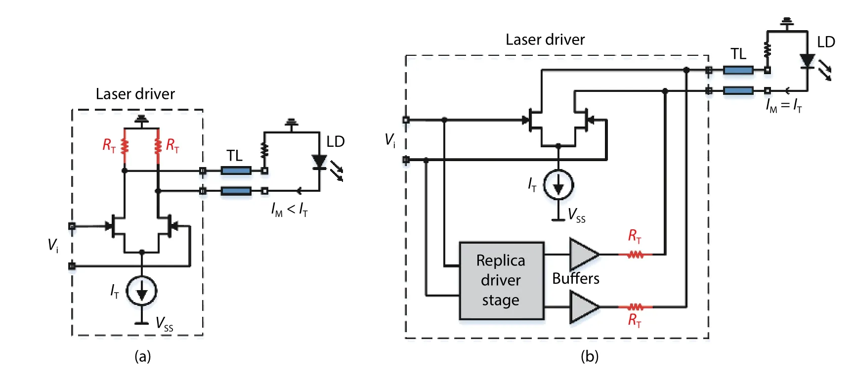
Fig. 1. LDD output stage: (a) with passive back termination, (b) with active back termination.
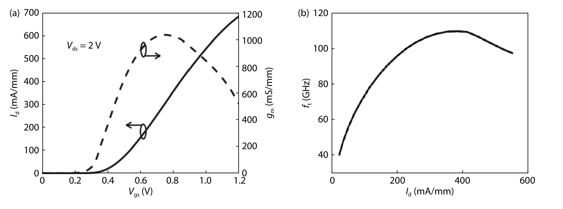
Fig. 2. (a) Id and g m versus V gs of pHEMT transistor. (b) ft in terms of Id.
Thirdly, LDDs are power-hungry circuits, especially at high output currents. Therefore, it is highly recommended to reduce the power dissipation of driver circuits to enable the realization of an air-cooled system and simplify the chip packaging[13].
Recently, several attempts with excellent results were reported for high current NRZ driver ICs implemented in various high-speed technologies. Using SiGe BiCMOS technology,an 80 mA laser driver operating at 1.25 Gbps, an 80 mA variable data rate driver (155 Mb/s to 4.25 Gbps), and a 50 Gbps optical transmitter with 40 mA output current were reported in Refs. [14, 10, 6], respectively. In pHEMT technology, a 10 Gbps modulator driver with 1.8 Vppsingle-ended output voltage and a 100 mA 10 Gbps laser driver with active back termination were proposed in Refs. [15, 9], respectively. On the other hand, the CMOS process can still compete to implement such circuits using broadband techniques like inductive peaking[3,5,12,16-18]and negative impedance converters[4,12,19]. These techniques improve the speed, especially when a high driving current capability is required. PAM4 driver ICs were also reported for low current vertical-cavity surface-emitting lasers (VCSELs), at 90 Gbps[20]and 56 Gbps[21]in SiGe BiCMOS technology and 25 Gbps in 90 nm CMOS[22],and high current distributed feedback (DFB) laser, at 30 Gbps in the 65 nm CMOS process[11].
This paper reports on the design, fabrication, and testing of a 15 Gbps-NRZ, 30 Gbps-PAM4 high current LDD implemented in a 0.15-μm GaAs pHEMT technology. The proposed driver is experimentally verified using a wire-bonded chip-on-board assembly. It can deliver a maximum modulation current of 120 mA to 25-Ω load.
2. Technology
The proposed LDD is designed and fabricated using the 0.15-μm GaAs E-mode pHEMT process. Besides the 0.15-μm E-mode transistor, the process also includes the following elements: PN junction diodes; 50 Ω/sq. tantalum nitride (TaN)thin-film resistors; 150 Ω/sq. active layer resistors; MIM capacitors with a density of 400 pF/mm2; round and square inductors; and two metal layers for interconnecting.
In Fig. 2(a), the variations of the drain current (Id) and transconductance (gm) with gate-source voltage (Vgs) of the pHEMT are shown. The maximum gmis 1000 mS/mm. The drain current is about 430 mA/mm at Vgs= 0.9 V. The typical threshold voltage (Vth) is 0.3 V. The characteristics of unity gain cutoff frequency (ft) in terms of Idis depicted in Fig. 2(b).It can be seen that the maximum ftis about 110 GHz. These results are promising enough to produce high-speed drivers that can deliver large output currents.

Fig. 3. Driver circuit architecture. (a) 15 Gbps-NRZ LDD with 80 mA output current (Slice I is enabled while slice II is disabled). (b) 30 Gbps(15 Gbaud/s) PAM4 LDD.
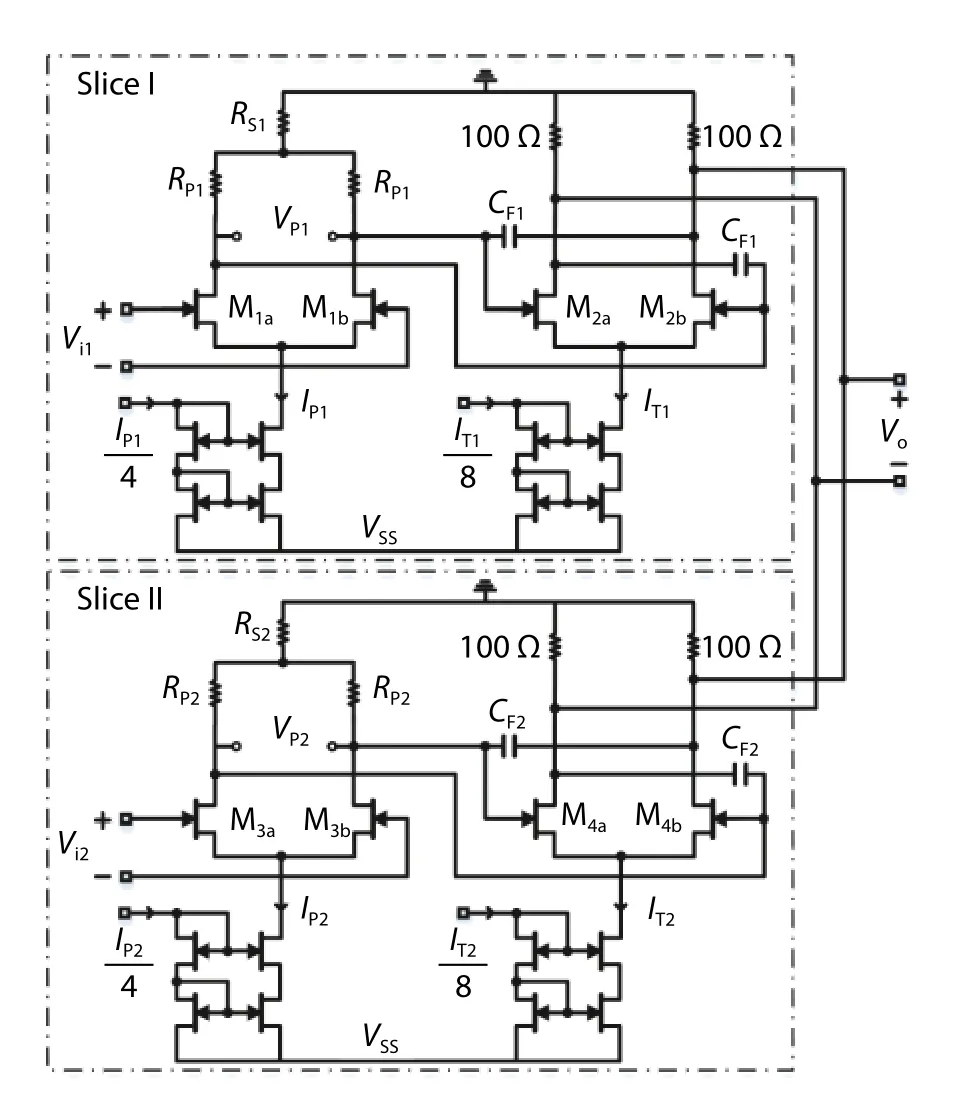
Fig. 4. Circuit diagram of the proposed driver.
3. Architecture and circuit design
The LDD architecture consists of two two-stage slices, as shown in Fig. 3. Each slice includes a pre-driver followed by an output driver, as schematically depicted in Fig. 4. The circuit is designed in a differential current mode logic (CML) topology due to its high speed and excellent immunity to switching noise, as the supply current is maintained relatively constant[1]. The circuit is powered using a single negative supply voltage (VSS) as shown in Fig. 4. A 100-Ω on-chip resistor is used across the output of each slice, producing a 50-Ω output back-termination impedance. Each slice presents a 50-Ωsingle-ended input impedance using on-chip resistors. The maximum tail currents, IT1and IT2, are 120 and 60 mA, and the corresponding output currents of slice I and slice II, when driving 25-Ω loads, are 80 and 40 mA, respectively. In this design, the cascode current mirror circuits are used to accurately adjust the tail currents due to their low systematic gainerror[23]. They also introduce a small output conductance,which improves the common-mode rejection ratio, and consequently, the driver circuit becomes less sensitive to common-mode noise.
The proposed driver can be used in two different functions: firstly, as illustrated in Fig. 3(a), each slice can operate as a stand-alone 15 Gbps-NRZ LDD with a maximum output current of 80 and 40 mA for slice I and slice II, respectively,when driving 25-Ω lasers. In this case, the NRZ input data is connected to the enabled slice while the other slice is deactivated. The output current can be boosted to 120 mA by simultaneously enabling the two slices and driving them with identical input signals.
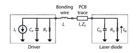
Fig. 5. Equivalent circuit of an LDD connected to an LD using wirebonded chip-on-board assembly.
Secondly, the circuit can work as a 30 Gbps (15 Gbaud/s)PAM4 LDD by combining the two 15 Gbps-NRZ drivers, as shown in Fig. 3(b). According to the possibilities of the most significant bit (Vi,MSB) and the least significant bit (Vi,LSB), 00,01,10, or 11, the output modulation current will be 0, 40, 80,or 120 mA, respectively. With the PAM4 modulation scheme,the transmission bit data rate is doubled at the same bandwidth compared to NRZ binary modulation.
3.1. Output impedance match
Fig. 5 illustrates a simple model of an LDD with passive back termination and the LD, where the LDD and the LD are connected using a wire-bonded chip-on-board assembly.Here, CPis the parasitic output capacitance of the driver, RTis the passive back termination resistor, L is the bonding wire inductance, CD, and RDare the parasitic capacitance and the equivalent input resistance of the LD, respectively. ITis the tail current of the driver and IMis the modulation current of the LD.RDequals 25 Ω and CDis assumed to be as low as 0.2 pF. The PCB trace is a 25-Ω microstrip TL (l = 5 mm), designed using Rogers material, which has a relative dielectric constant (εr) of 3.48. In this case, only CDdegrades the matching at the laser side, especially at high frequencies. Fig. 6 shows the 25-ΩS22curves, simulated at the LD side, at different RTand L values.Without RT, IMwill exactly equal IT, but the maximum S22in the frequency range from 0 to 15 GHz (S22,max) is about -0.03 dB, which seriously degrades the waveform fidelity. At perfect matching (RT= 25 Ω), IMis reduced to 0.5ITwhile a better S22performance is obtained especially at low L values. If RTis somewhat chosen to be greater than 25 Ω, IMwill be larger than 0.5IT(IMequals 0.667ITand 0.75ITwhen RT= 50 and 75 Ω, respectively) on the cost of degrading S22at low frequencies. However, S22performance at high frequencies may not be significantly impacted (or even improved) where the driver output impedance, parasitic capacitances, and inductances play a significant role[24]. When L = 0, 0.5, and 1 nH,S22,maxvalues at RT= 25, 50, and 75 Ω are (-12.9, -4, and -1.2 dB), (-7.4, -8.2, and -2.1 dB), and (-4.9, -6, -2.4 dB), respectively. At L = 0 nH, S22,maxat RT= 25 Ω is much lower than S22,maxat RT= 50 or 75 Ω. Whereas, when L = 0.5 nH or 1.0 nH,S22,maxvalues at RT= 50 and 75 Ω are better than the values obtained at perfect matching (RT= 25 Ω). These simulation results demonstrate that LDDs must employ output transmission line back-termination to absorb signal reflections from the laser side. A larger RTvalues could be used to reduce the waste in IM[8,24], especially when a good matching at the laser side is guaranteed. In the proposed design, a 50-Ω passive on-chip back termination resistor is utilized to balance between suppressing reflections and the loss in modulation current. It is worth mentioning that the TL is preferred to be as short as possible to reduce the insertion loss and propagation delay across it.
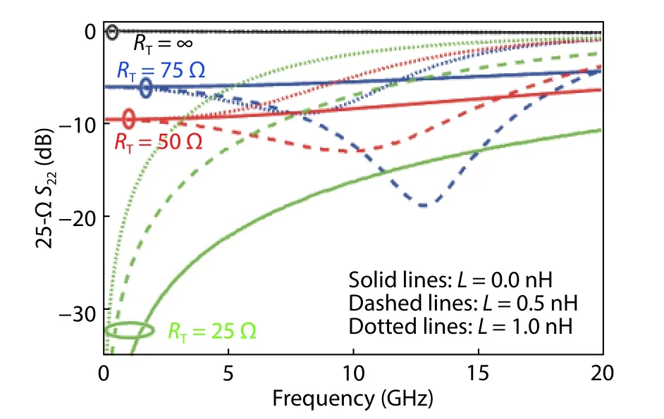
Fig. 6. (Color online) 25-Ω S 22 at different values of RT and L. Line patterns: solid, dashed, and dotted represent the 25-Ω S 22 curves at L = 0,0.5, and 1 nH, respectively. Line colors: black, blue, red, and green represent the 25-Ω S 22 curves when R T= ∞, 75, 50, and 25 Ω, respectively.Simulation results are obtained when C P= 0.2 pF, C D= 0.2 pF, and RD=25 Ω.
3.2. Driver circuit design
For any CML circuits in cascade, the single-ended output voltage swing is relatively small, less than Vthpeak-to-peak[25],to keep the transistors of the differential pairs in saturation,and consequently guarantee a high-speed operation. In the proposed circuit, the maximum single-ended output voltage of the output driver (Vo) equals 3 Vppwhen the output current is 120 mA. Therefore, a series resistor (RSi) is utilized in the pre-driver stage as a level shifter that reduces the common-mode output voltage at VPifrom (- IPiRPi/2) to(-IPiRPi/2-IPiRSi). Consequently, the output voltage swing of the output driver stage can be higher than Vth. An alternative solution to provide a high output voltage is to use level shifter stages, connecting between the pre-driver and the output driver[7,13,26]. Despite the buffering effect introduced by these stages, they significantly increase the power consumption of the driver circuit.
Focusing on slice I and considering the case at which the two slices are enabled to drive a 25-Ω load, the following formulas must be satisfied to keep (M1a-M1b), (M2a-M2b), and the tail current sources IP1and IT1in saturation region:


where Vi1, Vi1,cm, VP1, and VOare the single-ended input voltage, the DC common-mode input voltage, the singleended output voltage of the pre-driver, and the output driver, respectively. Vknee,IP1and Vknee,IT1are the minimum required voltage to maintain the cascode current mirrors in saturation. VGS1and VGS2are the required gate-source voltages to make IP1and IT1equally divided between (M1aand M1b) and(M2aand M2b), respectively. The cascode current mirrors are sized such that Vknee,IP1and Vknee,IT1are less than 0.7 and 0.9 V,respectively. To operate near the maximum ft, VGS1and VGS2are assumed to be higher than or equal to 0.6 V, drain current density ≥ 170 mA/mm.
By substituting into Eq. (2) with the maximum possible VO, which is 3 Vppwhen both slices are simultaneously enabled, and Vthof 0.3 V, we get that IP1RS1must be higher than 2.7 V. From Eq. (3), Vi1,cmmust be 1.3 V above the VSSlevel. If IP1RS1, Vi1,cm, and VSSare set to 2.8, -3.8, and -5.2 V, respectively, VP1+Vi1/2 must be less than 1.3 V, as derived from Eq.(1). Vi1at which complete current switching in both the predriver and the output driver stages is required to be as low as 300 mVpp, and thereby VP1must be less than 1.15 Vpp.
In order to achieve complete current switching in the output driver stage, a large input swing (VP1) and/or wide transistors (M2a-M2b) are required. However, the circuit bandwidth is degraded as W2increases due to the corresponding large input capacitance. On the other hand, increasing the output swing of the pre-driver (VP1) , by increasing IP1and/or RP1, results in higher power dissipation and/or bandwidth degradation, respectively. Thus, the final choices of IP1, RP1, and W2are determined after a set of iterations to achieve complete switching at acceptable speed and power consumption.
The small-signal equivalent half-circuit of the proposed driver and a 25-Ω laser diode is shown in Fig. 7, when only slice I is enabled. Cgsi, Cgdi, and Cdbiare the gate-source,gate-drain, and drain-bulk capacitances of Mi. gmiis the transconductance of Mi. R1and C1are the single-ended input resistance and capacitance of the pre-driver stage. RP1and Rmare the resistive loads of the pre-driver and output driver, respectively. RDand CDrepresent the equivalent input resistance and the parasitic capacitance of the laser diode, and they account for 25 Ω and 0.5 pF, respectively. As the frequency response of the circuit is dominated by the output driver capacitances, the miller approximation capacitance of Cgd1is considered for simplicity, thereby C1=Cgs1+(1+∣AV,P∣)Cgd1and C2=Cgs2+Cdb1+Cgd1, where AV,Pis the pre-driver voltage gain. The small-signal transfer function of the circuit can be expressed as;where Roand Corepresent the parallel combination of (Rmand RD)and (CDand Cdb2), respectively. For b2≫4a, which is generally achieved for small values of CF1, the transfer function shows an overdamped behavior with three real left halfplane (LHP) poles;
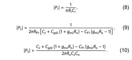


Fig. 7. The small-signal equivalent half-circuit for the proposed driver when only slice I is enabled.
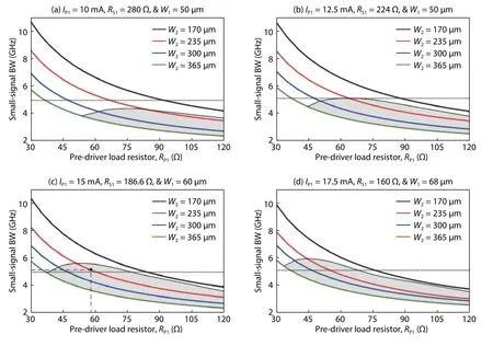
Fig. 8. Small-signal bandwidth dependence on RP1 and W2 at different IP1. Shaded areas represent the accepted values of RP1 and W2 at which VO exceeds 1.96 Vpp.
The numerator of Eq. (5) shows only one zero located at gm2/2π(Cgd2-CF1), which is substantially larger than the system poles. Generally, W2is larger than W1, and therefore∣P2∣≪∣P1∣. Moreover, at CF1= 0, ∣ P2∣ is much lower than ∣ P3∣,and the small-signal bandwidth (BW) approximately equals∣P2∣. Initially, CF1is assumed to be zero, and the values of IP1,RP1, and W2are chosen such that the small-signal BW is higher than 5 GHz, while complete current switching is achieved.Then, the BW will be boosted by adjusting CF1. Fig. 8 shows the BW dependence on RP1and W2at different IP1. The size of the pre-driver differential pair (W1) is chosen to guarantee complete switching of IP1corresponding to the 300 mVppsingleended input signal. The value of RS1is adjusted such that the voltage drop across it is about 2.8 V, as derived from Eq. (2).The shaded areas in Fig. 8 represent the accepted values of RP1and W2at which the output voltage of the output driver(Vo) exceeds 1.96 Vpp(98% of IT1passes through the ON transistor) when the input voltage equals 300 mVpp(single-ended).At IP1= 15 mA, the highest BW in the shaded area, whereVo>1.96 Vpp, exceeds 5 GHz (about 5.6 GHz), and this occurs at W2= 235 μm and RP1= 52.2 Ω. The parameters IP1, RP1, andW2are chosen to be 15 mA, 58 Ω (a little bit higher than 52.2 Ωto ensure that Vo> 1.96 Vppat different processes and temperature corners), and 235 μm, respectively, as shown in Fig. 8(c). At this point, VP1and Voequal 0.87 and 2 Vpp, respectively, and the small-signal BW is about 5.16 GHz.
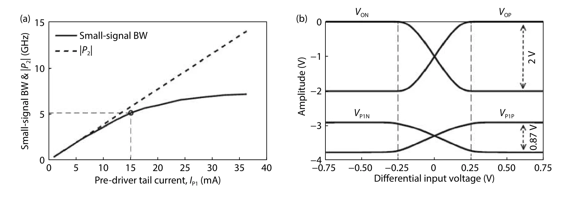
Fig. 9. (a) Small-signal BW and ∣ P2∣ dependence on I P 1, where V P1 is maintained constant at 0.87 Vpp. (b) DC transfer characteristics of the predriver and output driver.
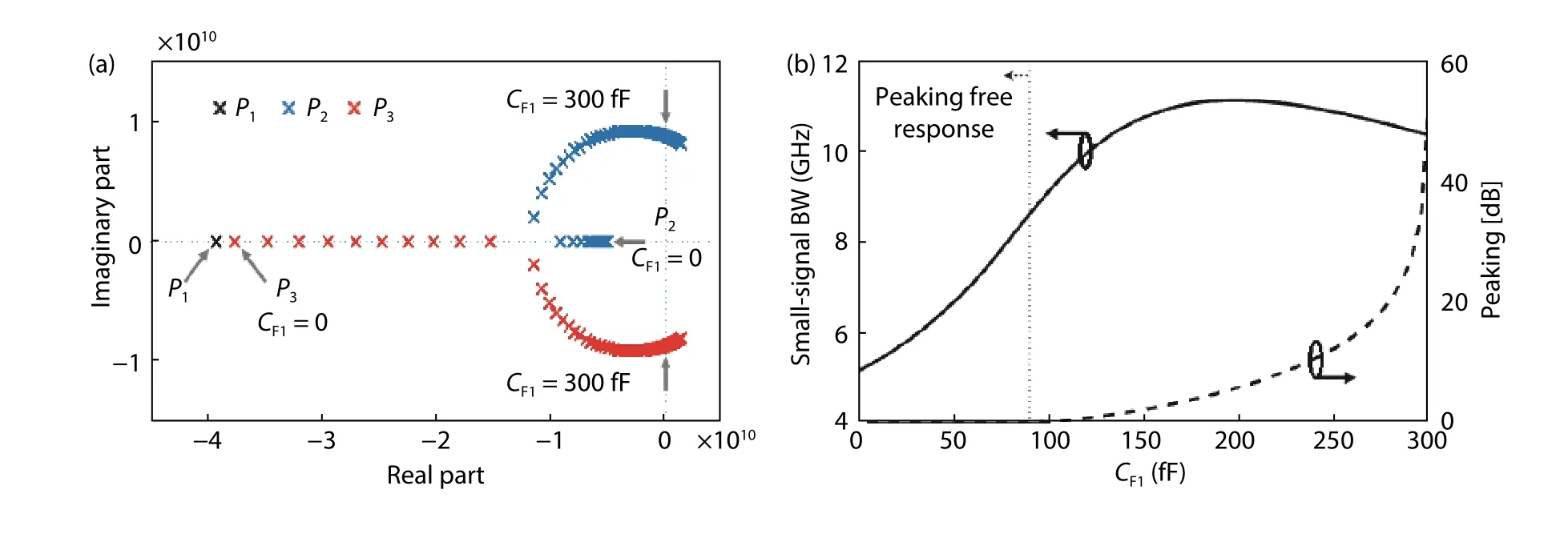
Fig. 10. (Color online) (a) Poles locus as C F1 varied from 0 to 350 fF. (b) Small-signal B W and peaking dependence on C F1.
Fig. 9(a) illustrates the dependence of BW and ∣ P2∣ on IP1,where VP1is maintained constant at 0.87 Vpp(RP1= 0.87/IP1)and W1is chosen to achieve complete switching of IP1through (M1a-M1b). At lower values of IP1, W1is much lower than W2, and consequently, the BW is dominated by ∣ P2∣.However, as IP1increases, W1and thereby C1increase accordingly. In this case, the pole introduced at the input of the predriver (P1) can no longer be ignored as it significantly degrades the circuit BW. So, at higher IP1values, a little improvement in the BW is achieved on the cost of higher power dissipation and area for the pre-driver circuit.
The dc transfer characteristic curves that show the voltage variations of the pre-driver and output driver output nodes in terms of the fully differential input voltage are shown in Fig. 9(b). It is clear that complete current switching,in the output driver stage, occurs at a differential input voltage of about 500 mVppd(250 mVppsingle-ended).
In the proposed design, the input capacitance effect of the output driver is reduced by using cross-coupled neutralization capacitors. The impact of these capacitors on the poles locus is illustrated in Fig. 10(a), where CF1is varied from 0 to 350 fF. The first pole (P1) is not altered by changing CF1as given in Eq. (8). As CF1increases, the dominant pole (P2) moves away from the origin, resulting in a higher bandwidth. Meanwhile P3moves towards the origin until reaching the breakout point, and then the two poles split out, producing an underdamped response. If CF1is further increased above 300 fF,P2and P3become positive, and an unstable system is obtained. Fig. 10(b) shows the small-signal BW and the peaking in the magnitude response dependences on CF1. For peakingfree frequency response, CF1must be below 90 fF. Fig. 11 shows the magnitude and group delay (GD) responses of slice I at different CF1values. The highest BW, without peaking, and the optimum GD response occurred exactly at CF1=90 fF. However, the chosen value of CF1must be below this bound to avoid any peaking in the magnitude response and large variances in GD when bonding wire inductance is accounted. In this design, a CF1value of 65 fF satisfies this condition.At this point, CF1equals approximately 126 % of Cgd2, and the input capacitance of the main driver is reduced by about 30%. Consequently, the small-signal BW of slice I is increased by 42.8% to reach 7.3 GHz.
Actually, the small-signal transfer function will be impacted in the existence of bonding wire inductance (L),which connects between the driver output and the LD. In this case, the system order is raised to five, and hence two additional complex conjugate poles are introduced. Fig. 12 shows the poles locus and the small-signal B W dependence on L, when CF1=65 fF and L is swept from 0.1 to 3 nH. Whereas, the magnitude and group delay responses at different values of L is illustrated in Fig. 13. However, the dominant pole (P2) moves towards origin as L increases, the BW slightly increases, as L varies from 0 to 0.5 nH, due to the high-quality factor of the complex conjugate poles (P4and P5) which introduces a peaking at their undamped natural frequency. If L is further increased above 0.5 nH, the BW decreases as the quality factor of (P4and P5) decreases such that it is no longer able to compensate for the decrease in P2, and thereby the BW is dominated by ∣P2∣. Also, group delay variances across the frequency domain are observed when L > 0.5 nH. Therefore, the bonding wiring inductance must be as small as possible to avoid the previous effects.

Fig. 11. (Color online) Slice I small-signal frequency response at different values of C F1. (a) Magnitude response. (b) Group delay response.

Fig. 12. (Color online) (a) Poles locus when C F1= 65 fF and L is swept from 0.1 to 3 nH. (b) small-signal BW dependence on L.

Fig. 13. (Color online) Slice I small-signal frequency response at different values of L for C F1= 65 fF. (a) Magnitude response. (b) Group delay response.
Fig. 14 shows the simulated 15 Gbps single-ended output eye diagrams at different L values. The input pattern is 27-1 pseudorandom bit sequence (PRBS) with a single-ended amplitude of 300 mVpp. A well-behaved time response, without ringing, overshoots, or undershoots, is observed for L <1 nH. The rise/fall times (20%-80%) at L = 0 nH equal 22/19.8 ps. At higher L values, the driver BW dramatically decreases, leading to higher rise/fall times and severe inter-symbol interference (ISI) as shown in Fig. 14(d).
The second slice is designed using the same previous procedure. With IP2, RP2, Rs2, W3, W4, and CF2of 12 mA, 68.75 Ω,233 Ω, 55 μm, 120 μm, and 30 fF, respectively, the small-signal bandwidth is about 8 GHz and the rise/fall times equal 16.5/15 ps.
4. Post-layout simulations
Large signal S-parameters characterization of the driver is performed at an input signal level of 0.6 Vppd(0.3 Vppsingleended), and the results are presented in Fig. 15(a). The forward-path gain (S21) curves demonstrate that the large signal bandwidth of slice I and slice II are 10 and 11.15 GHz, respectively. The input return loss is better than 10 dB up to 20 GHz for both slices. The output return loss is better than 10 dB up to 13.2 GHz. It is worth mentioning that both slices are required to produce similar group delay responses in the band of interest to avoid distortions in the output PAM4 signal.Fig. 15(b) shows the simulated group delay of both slices.The low-frequency group delay is about 34.5 and 33.7 ps for the MSB (slice I) and LSB (slice II) paths, respectively, and the peak difference is only 2.8 ps at 20 GHz.

Fig. 14. (Color online) Simulated 15 Gbps single-ended output eye diagram, when only slice I is enabled, at (a) L = 0 nH, (b) L = 0.5 nH, (c) L =1.0 nH, (d) L = 2.0 nH. Horizontal: time in ps, vertical: amplitude in V.

Fig. 15. (Color online) S-parameters simulation results. (a) Gain and return loss. (b) Group delay. S-parameters characterization is performed using a 100-Ω input port (fully differential), and a 25-Ω output port that is connected to one output terminal of the driver. Whereas, the other output terminal is connected to a 25-Ω dummy resistor.
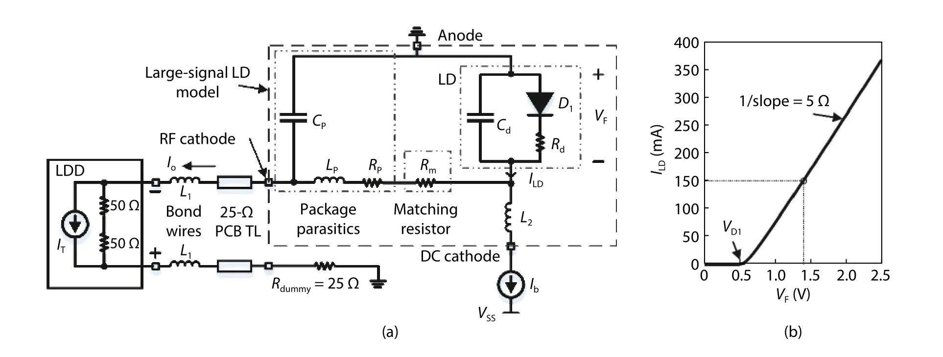
Fig. 16. (a) Large signal model of a DFB LD and its interface with the LDD chip. The LD parasitics Rd and Cd are accounted for 5 Ω and 4 pF, respectively. The package parasitics are assumed as R P= 1-Ω, L P= 0.15 nH, and C P= 0.5 pF. R m and L1 equal 20-Ω and 0.4 nH, respectively. (b) I-V characteristic curve of the LD showing that R d= 5 Ω, V D1= 0.51 V, and V F= 1.4 V at I LD= 150 mA.
The time-domain analysis was also performed to demonstrate the large-signal capability of the proposed driver. In this analysis, a large signal model of the laser diode, shown in Fig. 16(a), is utilized. The model consists of a forward-biased PN junction diode (D1) with its own parasitics (Rdand Cd), and the package parasitic elements, Rp, Cp, and Lp[27,28]. As most DFB lasers have a series resistance (Rd) of approximately 5-Ω,a series matching resistor (Rm) of 20-Ω is included in the laser package to provide a total input impedance of 25-Ω[24,29].The laser diode threshold current (Ith) and the forward voltage (VF) are assumed to be 10 mA and 1.4 V at 150 mA forward current, respectively. The I-V characteristic curve of D1,given in Fig. 16(b), shows that Rs= 5 Ω, D1forward voltage(VD1) is about 0.51 V at 1 mA forward current, and VF= 1.4 V at 150 mA forward current, which matches the assumed laser diode characteristics. The laser diodes are often biased above Ithto improve their speed[24], and thereby D1is DC biased with Ib= 25 mA. The RF cathode terminal of the LD model is DC-coupled to the inverting output terminal of the LDD chip through a bonding wire inductance (L1) and a 25-Ω microstrip PCB TL, while the non-inverting terminal is loaded with a 25-Ω dummy resistor. The length of the TL is 5 mm,and it is designed using Rogers PCB which has εr= 3.48.
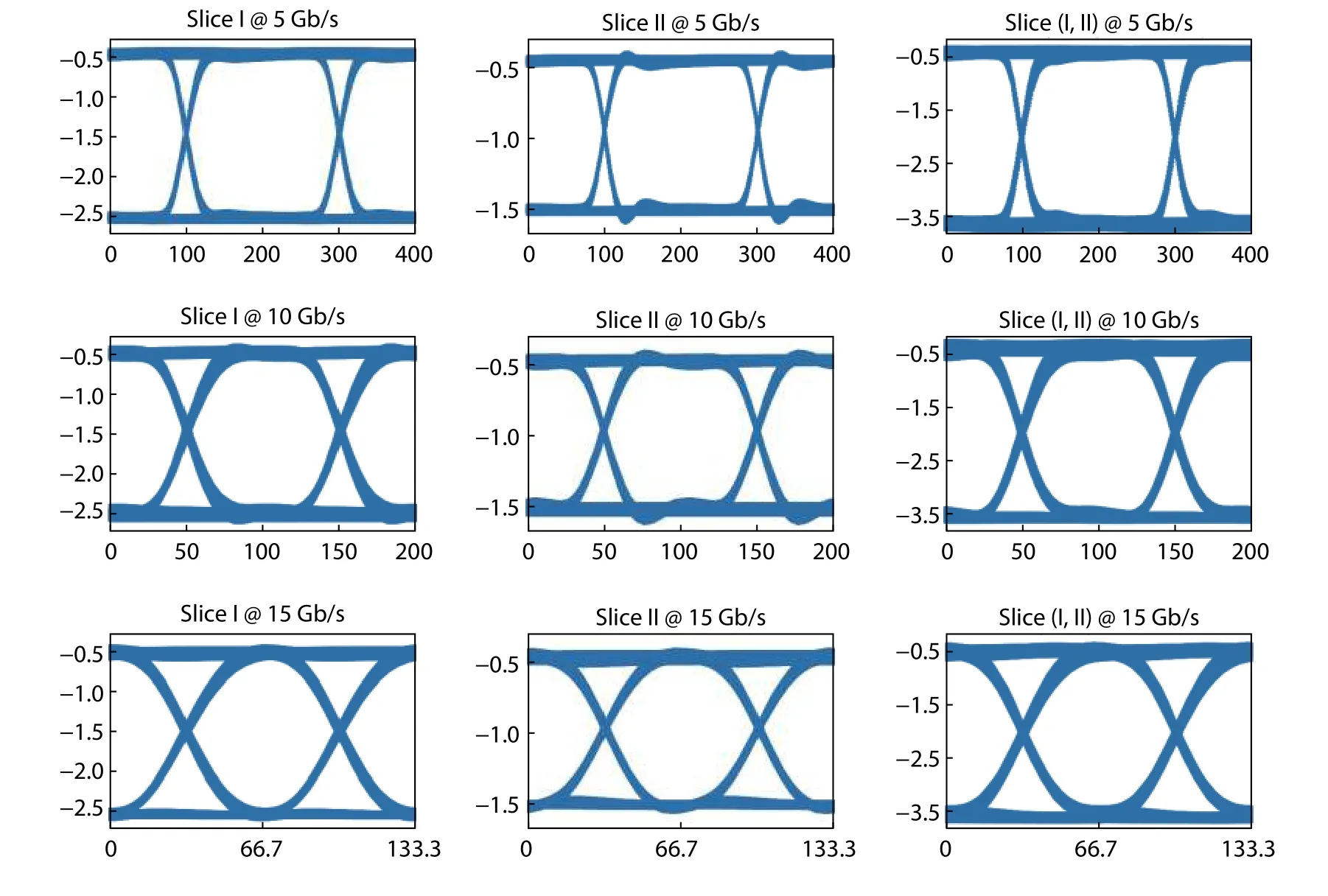
Fig. 17. (Color online) Simulated single-ended output eye diagrams for slice I, slice II, and both slices at different data rates. (Horizontal: time in ps, vertical: amplitude in V).

Fig. 18. (Color online) Simulated output PAM4 eye diagrams at (a) 10 Gbps (5 Gbaud/s), (b) 20 Gbps (10 Gbaud/s), (c) 30 Gbps (15 Gbaud/s). Horizontal: time in ps, vertical: amplitude in V.
The input pattern is a PRBS-7 signal with a single-ended amplitude of 300 mVpp. The simulated single-ended output eye diagrams at the RF cathode terminal of the LD model are illustrated in Fig. 17. The eye diagrams are obtained at different data rates when either slice is enabled or both slices are simultaneously enabled and driven by identical input patterns. Clear output eye diagrams are obtained at speeds up to 15 Gbps. The amplitude of the output eye diagram and the corresponding output current amplitude are (2 V and 80 mA) for slice I, (1 V and 40 mA) for slice II, and (3 V and 120 mA) for both slices, respectively. The rise/fall times at 15 Gbps for slice I and II are 24.2/23.3 ps and 19.3/18.5 ps, respectively.
If a simple resistive load was used, the high-level of the output eye diagrams, which occurs at zero output current,would be zero. However, when interfacing the proposed LDD, which has a 50-Ω single-ended output back termination, with the forward-biased LD model given in Fig. 16, the high-level values are shifted down to approximately -0.5 V,as shown in Fig. 17. Also, the low-level values are shifted down by the same amount. The proposed driver offers a sufficient output voltage compliance range that allows DC-coupling to 25-Ω lasers with output current up to 120 mA. With Vss=-5.2 V, simulation results reveal that the minimum voltage needed at the output of the driver for proper operation, achieving fast complete current switching, is about-3.65 V. Therefore, the allowable headroom for the laser and its matching resistor equals 3.65 V when the laser anode terminal is grounded. If the laser anode terminal is powered from a positive supply voltage (VDD), the output headroom will increase to VDD+ 3.65 V, at the cost of increasing the power dissipation.
Fig. 18 shows the output eye diagrams when the driver is used as a PAM4 transmitter at different data rates. A PRBS-7 pattern is applied to slice I while slice II is supplied with a one-bit delayed replica of the same pattern. Clear PAM4 eye diagrams are obtained at speeds up to 30 Gbps (15 Gbaud/s).The output voltage levels are -0.5, -1.5, -2.5, and -3.5 V, and consequently the peak-to-peak output voltage and current are 3 V and 120 mA, respectively.
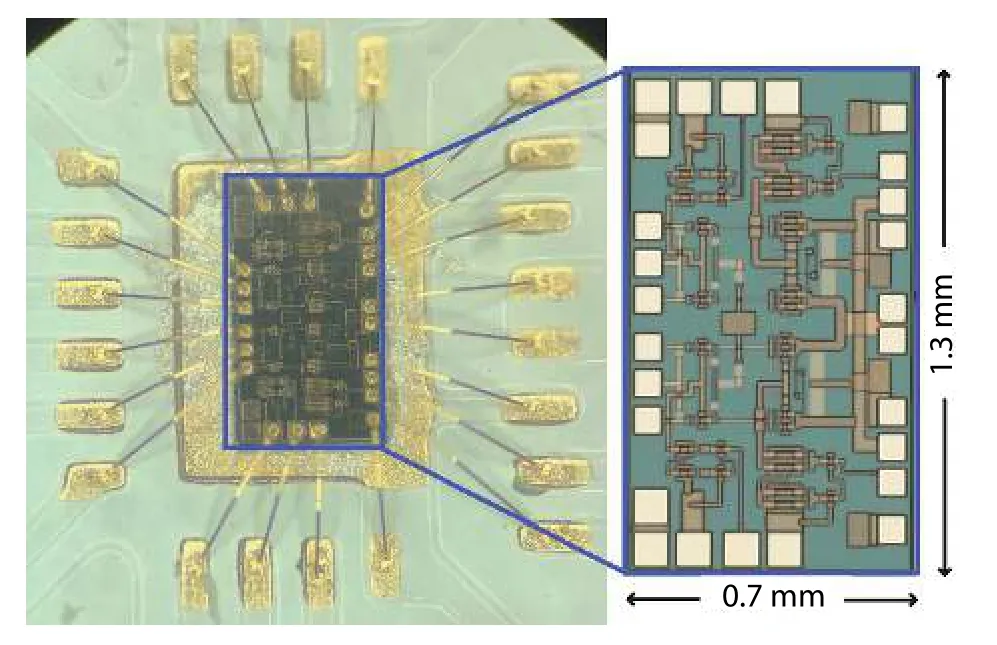
Fig. 19. (Color online) Photograph of the laser driver chip after wire bonding on a custom-designed PCB.
The design reliability is verified by checking the circuit performance at different process corners, supply voltage (±10%),and temperatures (from -40 to 125 °C), (PVT analysis). The output eye diagram features, for slice I and slice II, at 15 Gbps are summarized in Table 1. The results demonstrate that the eye diagram features are almost acceptable.

Table 1. Proposed driver performance at 15 Gbps when operated at different PVT corners.
5. Experimental results
The proposed driver is fabricated in a 0.15-μm GaAs Emode pHEMT process. The chip occupies a total area of 0.7 ×1.3 mm2. The die photograph and its corresponding bonding wire to a custom-designed Rogers PCB (εr= 3.48) are shown in Fig. 19. Two pads are assigned for each output terminal of the driver to reduce the bonding wire inductance. Gold bonding wires with aa 25.4 μm diameter were used, and the output bonding wires' lengths are less than 0.8 mm. Using the rule of thumb of 1 nH/mm, the estimated output bonding wire inductance will be less than 0.4 nH. With this low bonding wire inductance, the circuit performance will not be substantially affected, as discussed in Section 3.2.
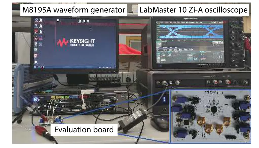
Fig. 20. (Color online) Experimental setup for eye diagram measurements.
Low-dropout (LDO) regulators are used to generate the required supply voltage and biasing to the chip. The ground bounce noise caused by supply bonding wires is suppressed by using localized decoupling networks, consisting of ferrite beads and ceramic capacitors. These components are mounted near the chip on the bottom side of the evaluation board. Both of the input connectors and the output load are placed as near as possible to the chip to reduce the traces’lengths. The input signals are AC coupled to the chip using 0.1 μF coupling capacitors. Each output terminal of the driver is DC coupled to a 25-Ω resistive load that is formed of two parallel-connected high-frequency 50-Ω resistors. The input traces are designed as 100-Ω differential transmission lines,while the output traces are considered as short interconnects due to the difficulty of designing 25-Ω PCB transmission lines. The electrical length of the input and output traces are 18.7 and 3.5 mm, respectively.
Fig. 20 shows the measurement setup of the proposed driver. The input pattern is a PRBS-31 with a single-ended amplitude of 300 mVpp(at the chip inputs), generated from a Keysight M8195A arbitrary waveform generator. The LabMaster 10 Zi-A high-speed oscilloscope, along with its active probe,is used to measure the eye diagram of the output signal.
Fig. 21 shows the measured single-ended output eye diagrams at different data rates when either slice is enabled or both slices are simultaneously enabled and driven by identical input patterns. Clear open eyes are obtained up to 15 Gbps. The rise/fall times (20%-80%) at 15 Gbps are below 25 and 20 ps for slice I and slice II, respectively. The eye amplitude equals approximately 2 V for slice I and 1 V for slice II at different data rates. Hence, it could be deduced that the output modulation current is 80 and 40 mA, respectively. When both slices are enabled and driven with the same input pattern, the output current reaches 120 mA with an output eye amplitude of about 3 V.
At 15 Gbps, the eye width and height are 0.531 UI and 1.4 V for slice I, and 0.518 UI and 0.68 V for slice II. The random jitter (Rj,RMS) and the deterministic jitter (Dj) is about(0.014 and 0.376 UI) for slice I and (0.015 and 0.388 UI) for slice II. Consequently, the measured total jitter at a bit error rate of 10-12(Tj@ BER = 10-12) equals 0.577 and 0.598 UI for slice I and slice II, respectively. When both slices are simultaneously enabled, Rj,RMS, Dj, and Tjare 0.012, 0.354, and 0.526 UI, respectively. Meanwhile, the eye width and height are 0.533 UI and 2 V. Most of the jitter observed in the measurement results arises from the pattern generator, cables, connectors, PCB TLs, and oscilloscope. The fully differential input eye diagram, measured at the output terminals of the coupling capacitors, shows high jitter levels (Rj,RMS= 0.03 UI, Dj= 0.297 UI, and Tj= 0.717 UI @ BER = 10-12) as depicted in Fig. 22. Consequently, this input jitter severely degrades the output jitter performance of the driver at 15 Gbps.
Fig. 23 shows the output eye diagrams of the proposed driver when it is tested as a PAM4 transmitter at different data rates. In this test, the two slices are activated and a PRBS-31 pattern is applied to slice I (MSB path) while slice II(LSB path) is supplied with a one-bit delayed replica of the same pattern. The results demonstrate that the PAM4 eye diagrams still keep open and clear up to 30 Gbps (15 Gbaud/s)with a peak-to-peak amplitude of about 3 V (single-ended).

Fig. 21. (Color online) Measured output eye diagrams for slice I, slice II, and both slices at 5, 10, and 15 Gbps. Horizontal scale: 33.4 ps/div for (a, b,and c), 16.7 ps/div for (d, e, and f), and 11.1 ps/div for (g, h, and i).
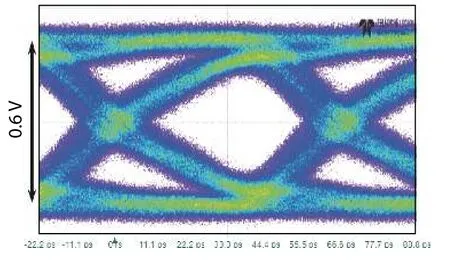
Fig. 22. Fully measured differential input eye diagram at 15 Gbps. Horizontal scale: 11.1 ps/div.

Fig. 23. (Color online) Measured PAM4 output eye diagram at (a) 10 Gbps (5 Gbaud/s), (b) 20 Gbps (10 Gbaud/s), (c) 30 Gbps (15 Gbaud/s). Horizontal scale: 33.4, 16.7, and 11.1 ps/div for (a), (b), and (c), respectively.
Table 2 summarizes the performance of the proposed driver, along with that of prior works. In our design, the modulation current is as high as 120 mA, with a power consumption of 1.228 W from a single -5.2 V supply. The proposed driver has a better FOM1than prior works that operate at nearby speeds. It also shows a high output power to power dissipation ratio that is defined using FOM2. Ref. [4] has a slightly higher FOMs than the reported driver as it employs AC coupling to interface the output load, which helps to reduce the supply voltage, and hence the power consumption is also reduced. However, the AC coupling technique requires discrete off-chip coupling components, which causes signal distortion at high speeds and significantly degrades the driver gain at low frequencies[19]. Ref. [11] also shows a higher FOM1than the proposed driver in NRZ mode. The reason is that Ref. [11] adopts the ABT technique which reduces the power dissipation on the expense of higher area. Also,the driver circuit in Ref. [11] is powered from three different supply voltages (1.2, 1.5, and 3.3 V), compared to a single supply in the reported driver. The reported modulation currents of the PAM4 driver in Ref. [21] and the NRZ driver in Ref. [30]are as low as 6.4 and 6.6 mA, respectively, making them only suitable for low current VCSEL diodes. As the modulation current decreases, the output voltage swing decreases, and consequently a lower supply voltage could be used. Therefore,the power consumption is significantly reduced as both of the total current and supply voltage are reduced, leading to a higher FOM1. Moreover, smaller output transistors can be used, leading to higher speed operation. Therefore, it is unfair to directly compare FOM1of driver circuits with widely separated modulation currents. Nevertheless, the proposed NRZ/PAM4 driver has the highest modulation current with a better output power to power dissipation ratio (FOM2), and it is still showing a comparable FOM1with these low current drivers. These results demonstrate the potential of the implemented driver to drive high current DFB lasers.
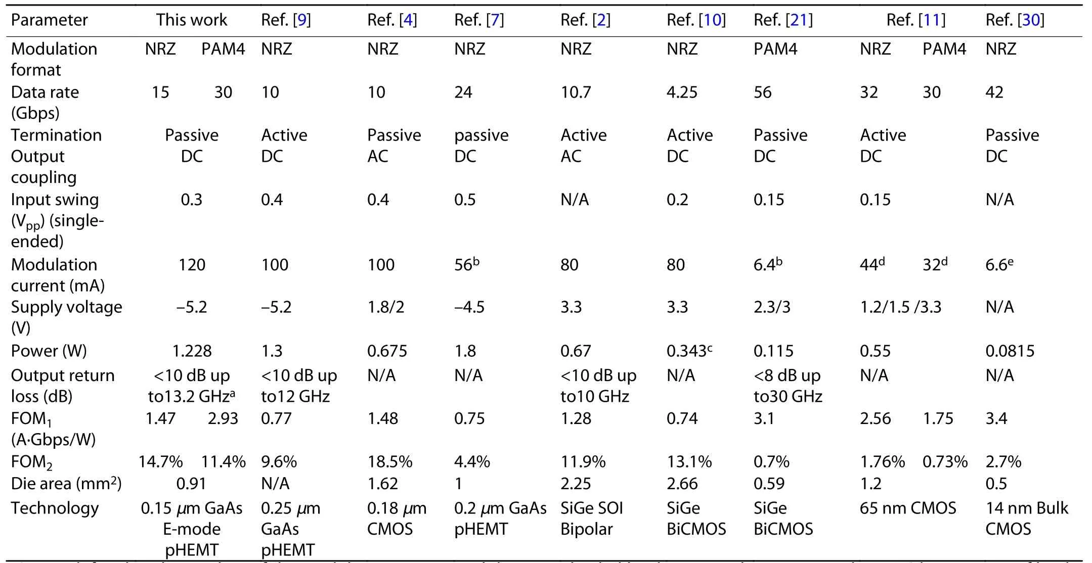
Table 2. Performance summary and comparison to prior work.
6. Conclusion
In this paper, the performance of a 0.15-μm GaAs pHEMT laser driver IC has been demonstrated. The driver supports both NRZ and PAM4 modulation schemes. A detailed design procedure was presented to optimize the driver circuit to achieve complete current switching at acceptable speed and power dissipation with a well-behaved transient response.The IC provides clear output eye diagrams at speeds up to 15 Gbps with NRZ and 30 Gbps (15 Gbaud/s) with PAM4 when driving 25-Ω loads. The reported driver demonstrates a high current driving capability along with better output power to power dissipation ratio, which makes it a good choice in driving high current DFB lasers.
Acknowledgements
The authors would like to acknowledge the support of the Chinese Academy of Science and The World Academy of Science (CAS-TWAS). In addition, they would like to thank the Information Science Laboratory Center of the University of Science and Technology of China for EDA tools. The work is partially carried out at the USTC Center for Micro and Nanoscale Research and Fabrication.
 Journal of Semiconductors2021年7期
- Journal of Semiconductors的其它文章
- Fabrication, characterization, numerical simulation and compact modeling of P3HT based organic thin film transistors
- The investigation of DARC etch back in DRAM capacitor oxide mask opening
- Fiber coupled high count-rate single-photon generated from InAs quantum dots
- Structural and electrical characterization of Cu2ZnSnS4 ingot material grown by melting method
- High room-temperature magnetization in Co-doped TiO2 nanoparticles promoted by vacuum annealing for different durations
- Regulation of the order-disorder phase transition in a Cs2NaFeCl6 double perovskite towards reversible thermochromic application
