Structural and electrical characterization of Cu2ZnSnS4 ingot material grown by melting method
S. Kerour , A. Bouloufa , , M. Lasladj , K. Djessas, and K. Medjnoun
1Département d’électronique, Faculté de Technologie, Université Ferhat Abbas Sétif-1, 19000 Sétif, Algeria
2Laboratoire d’Electrochimie et Matériaux, Université Ferhat Abbas Sétif-1, 19000 Sétif, Algeria
3Laboratoire PROMES-CNRS, Université Via Domitia Perpignan, 66100, France
Abstract: In this work, a Cu2ZnSnS4 (CZTS) ingot is grown via a melting method, then cooled; the resulting molten stoichiometric mixture is sealed off in a quartz ampoule under vacuum. The CZTS powder chemical composition analyses are determined using energy dispersive spectroscopy, and revealing the slightly Cu-rich and Zn-poor character of the ingot. Powder X-ray diffraction analysis reveals a crystalline structure with a kesterite phase formation, and a preferred orientation of (112) plane. The lattice constants of the a- and c- axes, calculated based on the XRD analyses, are a = 5.40 Å and c = 10.84 Å. Based on Hall measurements at room temperature, we find that the crystal exhibits p-type conductivity, with a high concentration of 1018 cm-3, a resistivity of 1.7 Ω cm, and a mobility of 10.69 cm2V-1s-1. Activation energies are estimated based on an Arrhenius plot of conductivity versus 1/T, for a temperature range of 80-350 K, measuring 35 and 160 meV in low- and high-temperature regimes, respectively, which is attributed to complex defects (2CuZn+SnZn) and antisite defects (CuZn), respectively. The observed scattering mechanisms are attributed to ionized impurities and acoustic phonons at low and high temperatures, respectively. The extracted band-gap is 1.37 eV.
Key words: Cu2ZnSnS4; growth; melting method; kesterite; Hall measurements
1. Introduction
Solar energy is probably one of the promising renewable resources, and is currently attracting a great deal of attention[1]. In recent years, CuInxGa1-xSe2(CIGS) thin-film solar cells have achieved a record conversion efficiency of 22.9%[2]up to as much as 23.35%[3]. Unfortunately, the scarcity of Indium, and the high cost of both indium and gallium resources could severely impede CIGS solar cell efficiency in the near future[4]. It is therefore necessary to establish a novel, earth-abundant, and low-cost absorber material for next-generation solar cells. Recently, Cu2ZnSnS4(CZTS),Cu2ZnSnSe4(CZTSe), and Cu2ZnSn(S,Se)4(CZTSSe) quaternary compounds have been recognized as among the most attractive materials for large-scale future deployment[5-8].CZTS is a p-type semiconductor kesterite crystalline structure,with a high absorption coefficient of 104cm-1in the visible range of the spectrum, and a direct bandgap, Eg, of about 1.45 eV[9-11]. Owing to the similarity of its physical properties to those of CIGS, as well as the relative abundance of its constituent elements, CZTS has become one of the most promising absorber layer materials for future photovoltaic applications[12-14]. Most recently, solar cells based on the alloy CZTSSe have achieved 12.6% power conversion efficiency[15].However, this is still lower than the Shockley-Queisser limit of 32%[16].
Despite the fact that the growth and characterization of CZTS single crystals have been the focus of several studies,achieving a better understanding of the fundamental properties of this material, in an attempt to achieve higher efficiency, remains challenging. In fact, CZTS single crystals have been prepared by various methods, such as the directional freezing method[17], solid state reaction[18,19], the traveling heater method[20,21]and the Bridgman technique[22]. Such processing techniques require costly and heavy equipment; as such, the melting growth technique may be advantageous for the growth of single crystals.
In this work, a low cost and simple technique based on thermal melt, which is widely used in the growth of high-quality single crystal of several photovoltaic absorbers[23-25], is used to grow a polycrystalline CZTS ingot. Growth parameters such as ampoule dimensions, process thermal profile, and the partial vapor pressure of the constituent elements are studied in depth in order for growth to succeed, and to achieve the best compound crystallization. The potential of the melt growth technique is assessed, along with the growth results,and the characterization of a CZTS single crystal. Compositional and structural properties are investigated in order to identify the obtained compound. The electrical properties are analyzed at low and high temperatures to gain further evidence as to the fundamental properties of the as-grown ingot.
2. Experimental details
2.1. Crystal growth
The CZTS single crystal was grown by cooling a molten stoichiometric of copper Cu (6N), zinc Zn (4N), tin Sn (5N) and sulfur S (5N) elements. The Cu : Zn : Sn : S constituents were weighed in 2 : 1 : 1 : 4 atomic proportions, placed into a quartz ampoule with dimensions of 200 mm length, and 14 mm diameter, and sealed off using an oxygen-acetylene blowpipe, under a pressure of 6.66 × 10⁻⁵Pa. The vacuum inside the ampoule was verified via high-voltage ionizing excitation. Fig. 1 shows the ampoule containing the constituent elements. The ampoule was then inserted into a horizontal tubular CARBOLITE furnace, connected to a temperature regulator. The mixture was heated from room temperature to 400 °C at a rate of 0.5 °C/min, and maintained at this temperature for 24 h, followed by an increase to 700 °C. This step was followed to suppress the potential explosive reaction occurring between S and the other elements. The ampoule was then heated to 1100 °C at a rate of 0.33 °C/min, and held at this temperature for 24 h to ensure the mixing and homogeneity of the melt. Heating to this high temperature reduces void formation in the ingot. Microcracking and bulk cracking are usually encountered if cooling rates are too high[26]. As such, the ampoule was slowly cooled to 900 °C, at a cooling rate of 0.166 °C/min, and maintained at this temperature for 12 h, followed by further cooling to 700 °C at the same rate in order to ensure successful crystal growth. For the temperature range from 700-300 °C, the cooling rate was increased to 0.5 °C/min. Finally, the furnace was switched off, allowing the ampoule to reach room temperature. The CZTS ingot removed from the ampoule measured about 25 mm. Using an agate mortar, the solid ingot was reduced into powder, so as to facilitate analysis of its various characterizations.
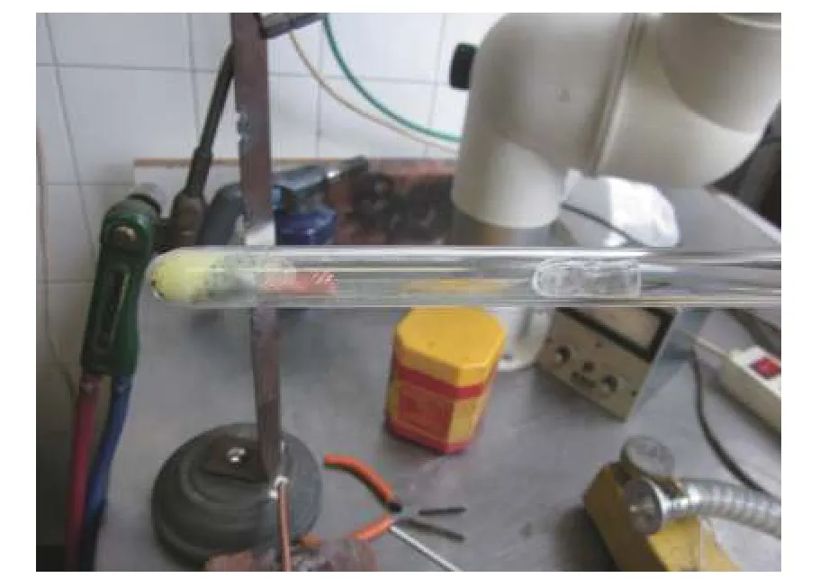
Fig. 1. The ampoule containing the constituent elements of CZTS under evacuation.
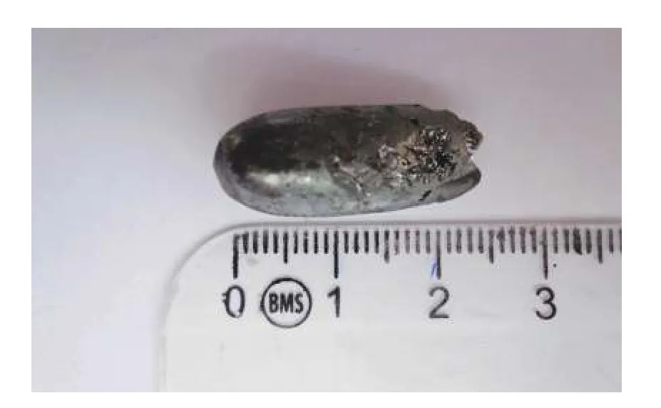
Fig. 2. The obtained ingot of CZTS.
2.2. Crystal characterization
The chemical composition of the powdered CZTS was analyzed by means of energy-dispersive spectroscopy (EDS) using a Jeol-JSM-6400 scanning electron microscope, operating at a 20 kV acceleration voltage. The crystal structure and lattice constants were examined via powder X-ray diffraction(XRD), where the pattern was collected using an Empyrean PANalytical powder diffractometer, with Cu Kαradiation (λ =1.54056 Å), and Bragg-Brentano θ-2θ focusing geometry. The XRD scan was conducted in the range of 2θ = 20°-80°, with a step width of 0.02°. Electrical transport properties were investigated using an Ecopia HMS 5300 Hall measurement system under a 0.56 T magnetic field in the Van der Pauw geometry.The temperature-dependence of the Hall Effect measurement was carried out over a temperature range of 80-350 K.Samples cut from the ingot, measuring 5 × 4 × 1.6 mm3were polished with 2400 to 4000 grain/cm2sandpaper with Al2O3powder, using a MICATECH Z34 polishing machine. Cu contacts of 0.8 mm of diameter were deposited onto the sample via Physical Vapor Deposition (PVD), to a thickness of 200 nm.These contacts were adequate for Van der Pauw measurements, although they were strictly Ohmic for p-type CZTS.
3. Results and discussions
3.1. Growth process
Growth of CZTS from the melt is complicated by major obstacles, such as the exothermic reactions of sulfur with other elements, and the increase in pressure during heating. This can lead to explosive fracture and loss of ampoules, and, in the worst-case scenario, loss of the furnace tube; it is therefore necessary to understand the reaction mechanisms. The partial vapor pressure of sulfur is of great importance in relation to the melting growth of CZTS bulk crystals. According to Ref. [27], it is given by the relation:

The pressure at 1100 °C reaches 6.3 × 10⁶Pa. This high pressure can lead to the explosion of the ampoule[28,29]. To avoid damage to the ampoule, it is therefore necessary to decrease the pressure inside it via the formation of binary and ternary sulfides, which have lower partial vapor pressure than sulfur[30]. Binary sulfides start to form from 213 °C for SnS[31],419 °C for ZnS[32], and 435 °C for CuS[33]. The CZTS phase formation occurs based on one of two reaction pathways[34]:

Fig. 2 shows the obtained 2.5 cm length ingot.
3.2. Composition analyses
EDS measurements were performed at multiple points along the ingot. Chemical composition as an atomic percentage is summarized in Table 1.

Table 1. Chemical composition of CZTS.
The average indicates the near stoichiometry of the ingot, with a slight deficiency in sulfur, due primarily to its volatility and high vapor pressure. The small quantity of remaining powder when introducing elements into the ampoule may be the cause of the slight deficiency in zinc. The EDS measurements show a Cu/(Zn+Sn) ratio of 1.26, and a Zn/Sn ratioof 0.88. Even this deviation from the stoichiometric ratios results mainly from a high population of intrinsic defects.Ref. [35] reported in their study that the cluster (2CuZn+SnZn)defect, which has a low formation energy (0.2-0.6 eV), should be the highest population defect, contributing to the high Cu/(Zn+Sn) and low Zn/Sn ratios. A typical EDS spectrum is acquired to investigate the homogeneity of elemental composition. The spectrum in Fig. 3 shows a uniform distribution of the ingot’s constituent elements.
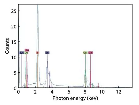
Fig. 3. EDS spectrum of CZTS ingot.
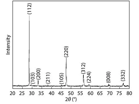
Fig. 4. Powder XRD pattern of the as-grown ingot.
3.3. Structural properties
The powder XRD pattern of the as-grown ingot is shown in Fig. 4. The strong diffraction peak around 2θ = 28.62° corresponds to the (112) crystal plane of the kesterite CZTS structure. Multiple reflection peaks, centered at 2θ = 33.1°, 47.62°,56.4°, and 76.58° correspond, respectively, to the (200), (220),(312) and (332) planes of kesterite CZTS (JCPDS card no. 026-0575).

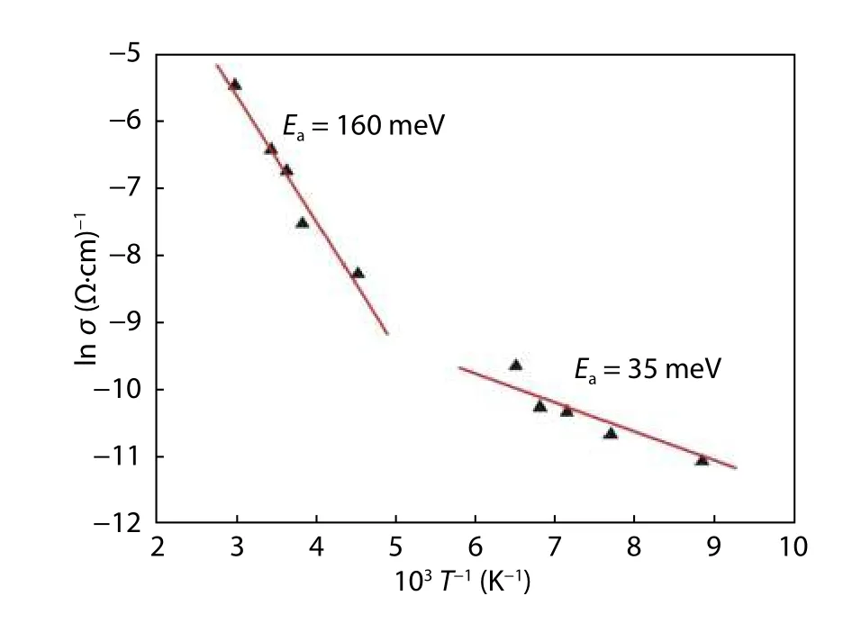
Fig. 5. Arrhenius plot of ln σ versus reverse temperature.
As CZTS has a tetragonal structure, the lattice constants of the a- and c- axes were calculated using Eq. (2):where d is the spacing between the planes, and (hkl) are the Miller indices. Lattice constants were found to be a = 5.40 Å,and c = 10.84 Å. Both of these results agree well with the reported values of a = 5.435 Å and c = 10.85 Å in Ref. [36], and a = 5.429 Å and c = 10.847 Å in Ref. [22]. Full width at half maximum (FWHM) was estimated using the mean derived from the Fytick software package[37]for the main characteristic peak (112) located at 28.62°, and measured 0.16°. This narrow FWHM indicates the high-quality single-crystalline nature of the synthesized ingot. No secondary phases, such as SnxSy,or Cu2-xS, were identified in the XRD pattern.
3.4. Electrical properties
The electrical properties of the samples were determined via Hall measurements at room temperature. The ingot was found to exhibit p-type conductivity. A high p-concentration of 1.29 × 1018cm-3, and a low resistivity, ρ, of 1.7 Ω cm were measured. This higher concentration has been widely reported in samples with the ratio Cu/(Zn+Sn) > 1, and is ascribed to the fact that the ionization of the intrinsic acceptor defects produces holes; a high population of defects results in high carrier concentration. Several previous results have indicated that resistivity decreases with an increasing Cu/(II+IV) atomic ratio in some Cu2-II-IV-VI4semiconductors,such as CZTS and CZTSe[38-40]. The hole mobility, μp, was then measured, and found to be 10.69 cm2V-1s-1. This value is in good agreement with that reported in the literature[41,42]. In order to investigate the properties of CZTS bulk crystal in more detail, the temperature dependence of Hall measurement was calculated for a temperature range of 80-350 K. Activation energies of 35 and 160 meV, for low- and high-temperature regimes, respectively, were extracted from the Arrhenius plot of ln σ versus 1/T (Fig. 5) using the Petritz model[43]:
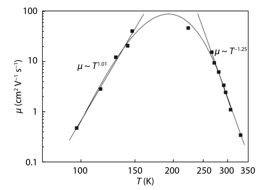
Fig. 6. Temperature dependence of mobility.
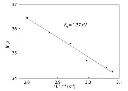
Fig. 7. Carrier concentration versus 1/T.

where σ is the conductivity, σ0is the pre-exponential term, KBis the Boltzmann constant, T is the absolute temperature, and Eais the activation energy related to the defects in the CZTS.An activation energy of 35 meV may be associated with the transition energy of shallow defects in the (2CuZn+SnZn)cluster; however, the activation energy in the high-temperature regime of 160 meV agrees well with the calculated (-/0)level of CuZnantisite acceptor defects (ionized from neutral to (-1) charge), as reported by Ref. [35]. In that study, the authors demonstrated that the presence of both (2CuZn+SnZn)and CuZnantisite defects in Cu-rich compounds corresponds to high carrier concentration (~ 1018cm-3). This value of concentration agrees well with the 1.29 × 1018cm-3measurement obtained for a CZTS single crystal in this work.
The charge carriers may be scattered by various mechanisms; as such the transport properties depend strongly on the type of scattering mechanism involved. Fig. 6 depicts the temperature- dependence of the mobility, in order to determine these mechanisms. In the low-temperature range below 150 K, the sample shows a power-law behavior, with an exponent of 1.01; this value would indicate that the dominant scattering mechanism is ionized impurity scattering. At higher temperatures (above 200 K), the mobility shows a steeper decrease, with a power-law exponent of -1.25, indicating that the mobility is dominated by acoustic phonon scattering[44,45].
As the semiconductor’s aspect at high temperatures seems intrinsic, the hole concentration is defined as:

Based on the linear region of the Arrhenius plot of carrier concentration versus T-1presented in Fig. 7, the band gap of CZTS was extracted, and was found to be 1.37 eV.This decrease is related to the effect of the cluster defect(2CuZn+SnZn) contributing to a slight band edge shift.
4. Conclusion
A Cu2ZnSnS4crystal ingot was successfully grown using the melting method. No secondary phases were observed,based on the XRD measurements. Structural analysis clearly revealed a crystalline tetragonal structure, corresponding to kesterite CZTS. Lattice parameters a and c of 5.40 and 10.84 Å, respectively, agree well with the known crystal lattice constants. The EDS measurements indicate the slight Cu-rich and Zn-poor nature of the ingot, with a Cu/(Zn+Sn) ratio of 1.26,and a Zn/Sn ratio of 0.88. The Cu content increment in the ingot is related to element losses during the heating process, owing to their high volatility. This result explains the high value of carrier concentration (1.29 × 1018cm-3) and the low value of the resistivity (1.7 Ω cm) obtained in this work. An Arrhenius plot of ln(σ) versus 1/T revealed two defect activation energies of 35 and 160 meV at low and high temperatures, respectively, which agrees well with the (2CuZn+SnZn) cluster shallow defects, and the calculated (-/0) level of CuZn, respectively. This cluster defect leads to a shift in the band edge, resulting in a decrease in the bandgap to 1.37 eV. The scattering mechanisms involved were discussed, and subsequently defined as ionized impurity scattering, and acoustic phonon scattering, for low and high temperatures, respectively.
Acknowledgements
The authors wish to thank Mr Jean-Luc Gauffier of the Physics Department, INSA, Toulouse, France. This work was supported by the Directorate-General for Scientific Research and Technological Development (DGRSDT-Algeria), in the context of Algerian-Tunisian cooperation.
 Journal of Semiconductors2021年7期
- Journal of Semiconductors的其它文章
- Blue perovskite LEDs
- ~1.2 V open-circuit voltage from organic solar cells
- Engineering microstructures for efficient Sb2(Sx Se1-x)3 solar cells
- Post-sulphuration enhances the performance of a lactone polymer donor
- Suppressed light-induced phase transition of CsPbBr2I:Strategies, progress and applications in the photovoltaic field
- Efficient MAPbI3 solar cells made via drop-coating at room temperature
