Fabrication, characterization, numerical simulation and compact modeling of P3HT based organic thin film transistors
Shubham Dadhich, A. D. D. Dwivedi, , and Arun Kumar Singh
1School of Electronics Engineering, Vellore Institute of Technology (VIT), Vellore, TN- 632014, India
2Department of Pure and Applied Physics, Guru Ghasidas Vishwavidyalaya Bilaspur (C.G.) 495009, India
Abstract: This paper presents the fabrication, characterization and numerical simulation of poly-3-hexylthiophene (P3HT)-based bottom-gate bottom-contact (BGBC) organic thin film transistors (OTFTs). The simulation is based on a drift diffusion charge transport model and density of defect states (DOS) for the traps in the band gap of the P3HT based channel. It combines two mobility models, a hopping mobility model and the Poole-Frenkel mobility model. It also describes the defect density of states (DOS) for both tail and deep states. The model takes into account all the operating regions of the OTFT and includes sub-threshold and above threshold characteristics of OTFTs. The model has been verified by comparing the numerically simulated results with the experimental results. This model is also used to simulate different structure in four configurations of OTFT e.g. bottom-gate bottom-contact (BGBC), bottom-gate top-contact (BGTC), top-gate bottom-contact (TGBC) and top-gate top-contact (TGTC) configurations of the OTFTs. We also present the compact modeling and model parameter extraction of the P3HT-based OTFTs. The extracted compact model has been further applied in a p-channel OTFT-based inverter and three stage ring oscillator circuit simulation.
1. Introducation
Organic electronics have received great attention since the initial discovery[1], due to the range of exotic mechanical properties of the organic semiconductor materials and technologies that they offer in contrast to prevalent inorganic semiconductor technologies. For example, plastics can be flexible[2], stretchable and processed from solution-phase over large areas in roll-to-roll newspaper-style printing[3,4]. Plastics can also be processed at lower temperatures[5], and hence have lower economic costs than silicon. Another benefit of synthetic polymeric materials is that their properties can be tailored via the introduction of different chemical groups that vary overall molecular structures, giving rise to the idea of“Make to Order” (MTO) electronics. Applications for organic thin film transistor (OTFT) include light-emitting devices[6-32],bioelectronics sensing devices and applications[6]that would require low amounts of computing, such as electronic tags or memory devices[7-9]. One of the primary focuses for organic electronics research over the past few decades has been the organic field-effect transistors (OFETs)[10-32]. OTFTs are a key element of organic electronics[1-32]. Whilst solution-processed OTFT[11-13]with desired mobility values have started to enter the realm of industrial application, they can’t be utilized unless the other critical parameters are also addressed.For example, TFTs can be used as switches in both voltage-driven and current-driven applications. Voltage-driven applications, such as liquid crystal displays or e-paper, require a controlled voltage to be applied. On the other hand, display technologies used active matrix organic light emitting diode(AMOLED) commercially for smart phones, laptops, tablets,games consoles, smart watches, digital cameras, media players and televisions are current-driven. In the development of TFT, the mathematical model of device represents an important bridge between manufacturing of semiconductor and circuit design. In past years, some mathematical models of OTFT were developed[14]. All these models describe dc current-voltage characteristics. These models are developed by slight modification in classical MOS transistor models. But these are not able to describe complete behaviour and unique features of OTFTs. During the design process to evaluate the circuit performance, compact model is necessary[12,28-32].Therefore, technology computer aided design (TCAD) simulation and compact modeling of organic thin film transistors[13-32]become very important. The researchers have put an extensive research effort into OTFT compact modeling for circuit simulation as in Refs. [28-32]. Further research efforts by various researchers are going on in this direction. In current scenario, a physical model based on organic semiconductor is required for analog and digital circuits. The developed model should have these qualities: (i) consistent behaviour, (ii) having parameter variable that can be put easily,(iii) symmetrical to OTFT structure, (iv) easily derivable and simple calculation, (v) reducible and upgradable, (vi) tunable for bad experimental data, and (vii) all the relations can be justified by physics. So in this work, we try to achieve all these qualities. The model based on fundamental semiconductor equations and drift diffusion charge transport model has been utilized for TCAD based numerical simulation. This approach and model has been successfully examined on experimental data and also extracted the performance parameters of the OTFTs for both saturation and linear region of operation of OTFTs. For compact modeling we used the UOTFT model which introduces general expression of modeling for conductivity of channel of OTFTs[31-33].
In this paper, we used Silvaco's ATLAS device simulator to use the charge carrier continuity equation, Poisson's semiconductor device equation[22-28]and drift diffusion model[22-28]to simulate electrical characteristics of the given device. Silvaco's UTMOST-IV model parameter extraction software has been used to obtain compact model parameters using the UOTFT model[28-32,38]. TCAD simulation results and compact model based simulation results were also compared with the measured results of experimentally fabricated device. This section talks about basic introduction. Experimental details of the fabricated P3HT based bottom-gate bottom-contact (BGBC) OTFT are given in Section 2. TCAD based numerical simulation and performance parameter extraction of the device are given in Section 3. In Section 4 we describe the results and discussions. Compact modeling, model parameter extraction and model validation are explained in the Section 5. Finally, conclusions drawn are given in Section 6.
2. Experimental details
2.1. OTFT fabrication
We fabricated a P3HT based bottom-gate bottom-contact (BGBC) OTFT as shown in Fig. 1. A n+type Si wafer with 1 × 1 cm2was chosen as the substrate. On the top of the wafer a 300 nm thick SiO2layer was already deposited. Substrates were cleaned with a mixture of hydrogen peroxide and ammonia solution with 5 : 1 ratios at 85 ˚C for 1 h. Further octyltrichlorosilane (OTS) was used to enhance ordering of P3HT polymer chains over the substrate. Gold (Au) metal was used as the source/drain electrodes. The 30 nm Au electrodes were thermally deposited using vacuum coating unit(HHV make Model: SMART COAT 3.0) through metal mask on wafer. The length of the channel was 50 μm and the width of the device was 2 mm. In our study, we have used P3HT having molecular weight of 37800 kDa and 90% head to tail regioregularity. Solutions of P3HT in choloroform (Merck, India)were prepared with 2 mg/ml concentration. The prepared solution was spin coated on wafer for 20 s at 6000 rpm using a spin coater (APEX instrument Co, India). The thickness of P3HT was maintained about 50 nm. Further, the sample waskept in an annealing chamber for 1 h at 80 ˚C to remove the solvent.
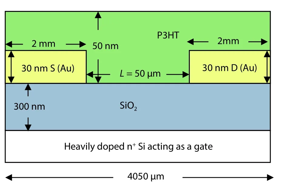
Fig. 1. (Color online) Structure of the P3HT-based bottom-gate bottom-contact (BGBC) OTFT.
2.2. Thin film characterizations and OFETs measurement
The UV visible absorption spectra of P3HT thin films over indium thin oxide (ITO) coated glass were measured by a UV-Vis. spectrophotometer from PerkinElmer, Germany (model no. Lamda 25). The morphologies of P3HT films on SiO2/Si substrate were performed using atomic force microscopy(AFM) (NT-MDT, Russia model Pro 47). All electrical measurements of OFETs were conducted under ambient conditions using an HP semiconductor parameter analyzer (Model No.4145B) from Hewlett-Packard, USA.
The transfer (IDS-VGS) characteristics were extracted at a different drain-to-source voltage (VDS); these were -15, -30, -45,-60 V voltages. The gate to source voltage (VGS) was swept from +20 to -40 V by step of 1 V. To calculate threshold voltage IDS1/2vs VGSwas plotted and extrapolated on VGSaxis for VDS= +15 V. A positive value shows that the device was performing in depletion mode. The Coxcapacitance of per unit area was measured as 10 nF/cm.
3. TCAD based OTFT device modeling and numerical simulation
3.1. Device simulation using ATLAS Technology Computer aided design (TCAD) Simulator
For modeling and simulation, the ATLAS device simulator has been opted for[16]. For technology computer aided design (TCAD)-based simulation we used Silvaco's ATLAS device simulator to use the charge carrier continuity equation, Poisson's semiconductor device equation[22-28]and drift diffusion model[22-28]to simulate electrical characteristics of the given device. For simulating the electrical characteristics of the OTFT we created the similar device structure in the DeckBuild window, as shown in Fig. 1, with the same device dimensions as in the case of the fabricated device.
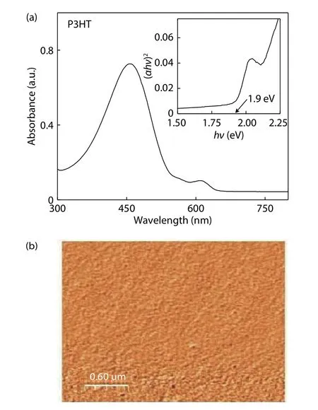
Fig. 2. (Color online) (a) UV-Vis spectra of P3HT thin film on glass[(αhυ)2 versus hυ plot has been shown in the inset] and (b) AFM image of P3HT thin film on the SiO2/Si substrate.
3.2. Material parameters for TCAD based numerical simulation of P3HT based OTFTs
In this paper, P3HT is the semiconductor material used as channel of the OTFT. The material parameters for P3HT used in the TCAD simulation are listed in Table 1 as given below.
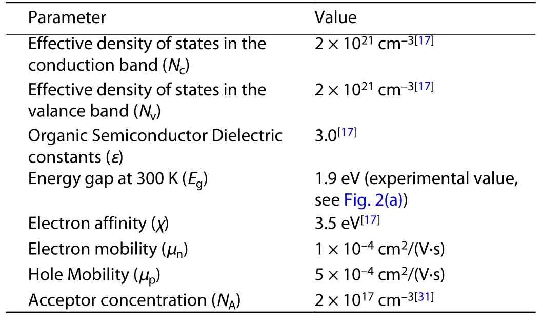
Table 1. Material parameters for P3HT.
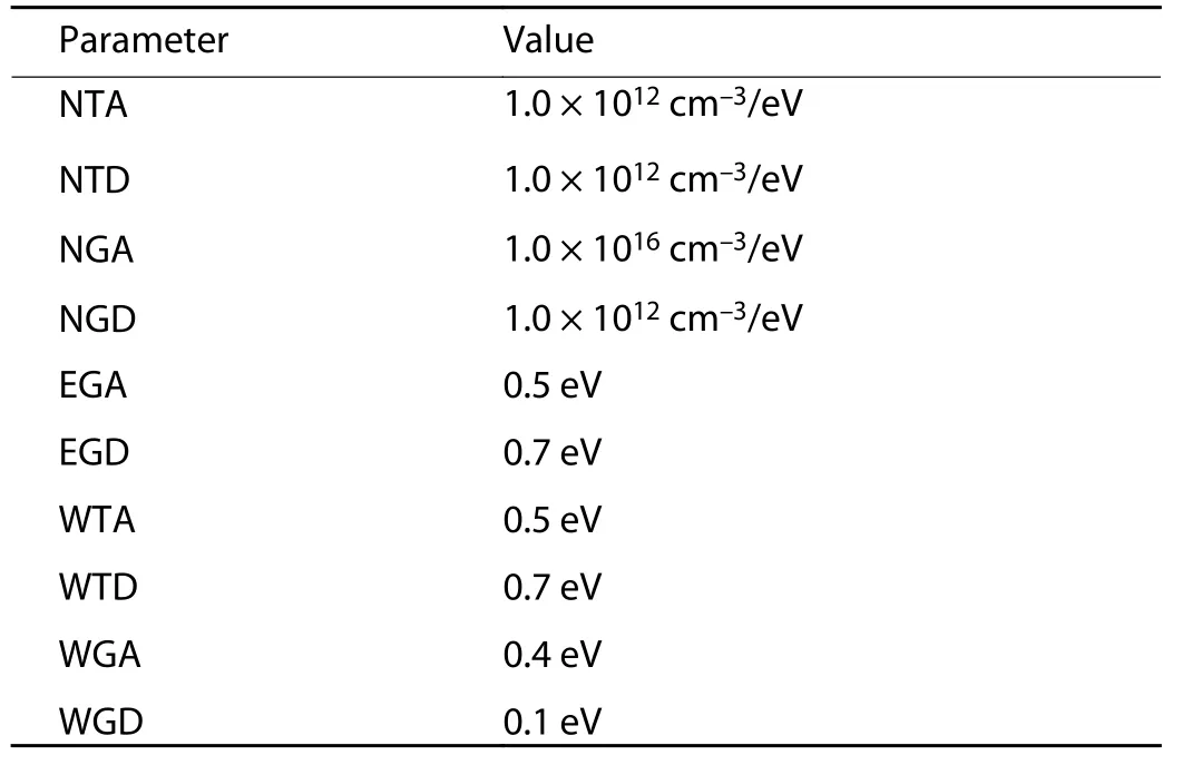
Table 2. DOS parameter for P3HT-based OTFT.
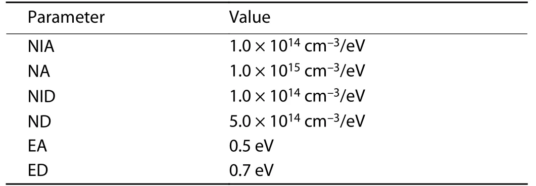
Table 3. Double peak DOS parameter for P3HT.
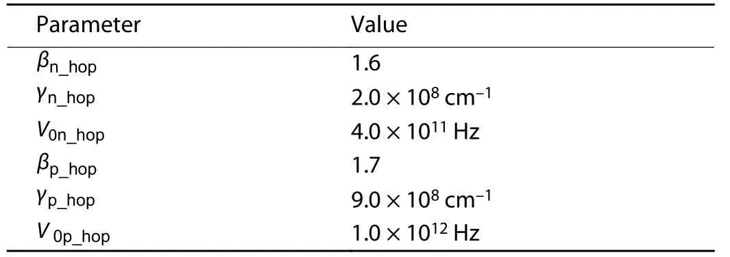
Table 4. Hopping mobility model parameters of P3HT.
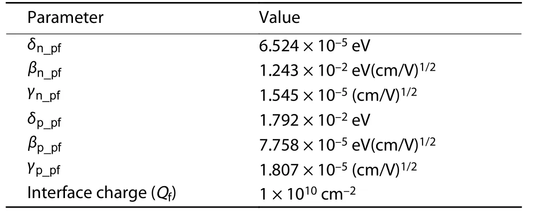
Table 5. Pool-Frenkel mobility model parameter for P3HT-based OTFT.

Table 6. Performance parameters of simulated P3HT based OTFTs.

As shown in Eq. (1), NCand NVdirectly affect the electrons and holes concentrations i.e. n and p. EFis Fermi level and ECis minimum energy of conduction band and EVis maximum energy of valance band. TLis temperature as typically 300 K and k is the Boltzmann constant. Here acceptor concentration is doping concentration. When doping concentration is increased, the drain current also increases.
3.3. Defect density of states (DOS)
In disordered organic semiconductor material various defects states are present in the band gap that trap the charge carrier. So we have included energy distribution of defect states also. The total density of defect states (DOS) g(E) also governs the properties of OTFTs, is modeled as consisting of four constituents, i.e a donor-like exponential band tail function gTD(E), an acceptor like exponential band tail function gTA(E), a donor like Gaussian deep state function gGD(E) and an acceptor like Gaussian deep state function gGA(E), where E is the trap energy. Its energy distribution definition is essential to acquire exact electrical property. The subscripts T stands for tail, G stands for Gaussian, A stands for acceptor and D stands for donor.
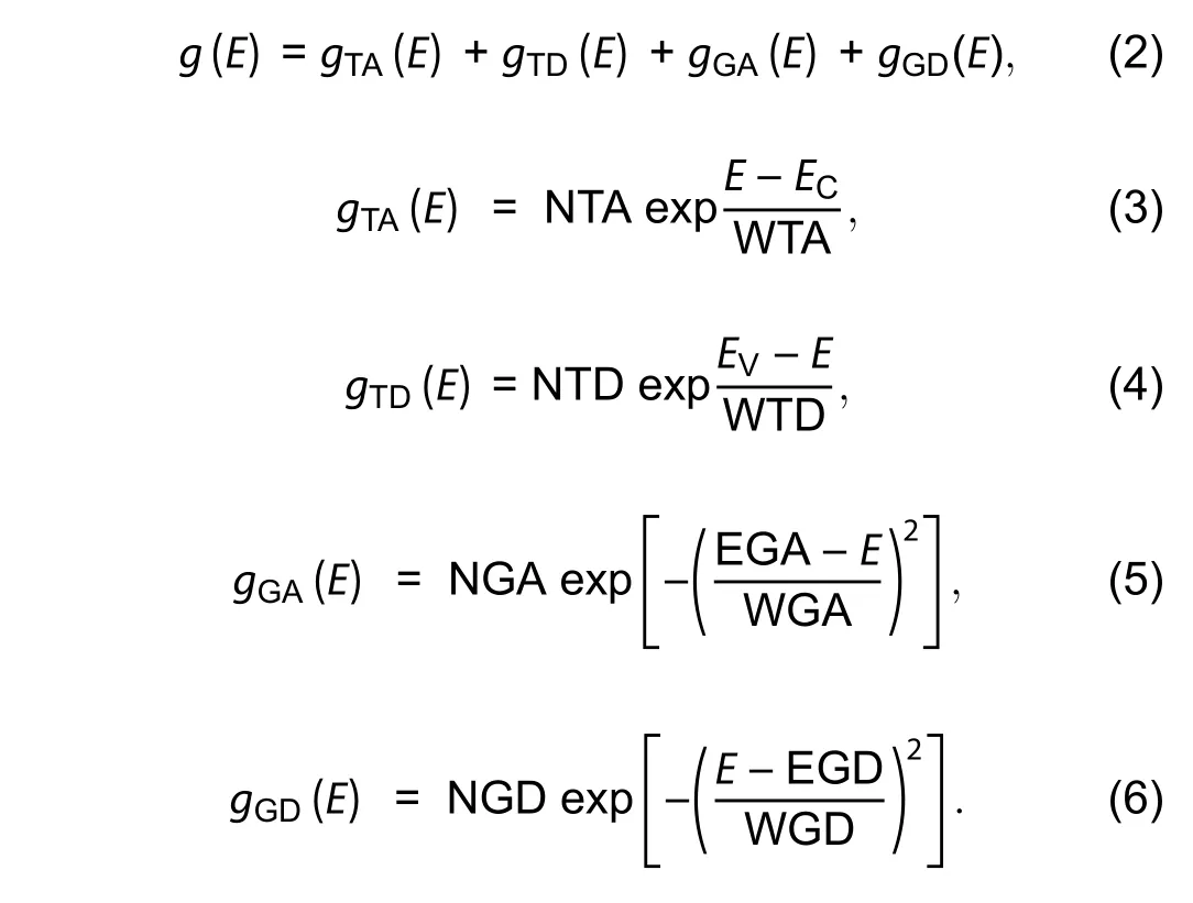
NTA and NTD denote edge intercept densities of valence and conduction band with exponential tail distribution. Its characteristic decay energy is WTA and WTD. NGA and NGD denote total density of state with Gaussian distribution and its peak energy distributions are EGA and EGD, respectively.Its characteristic decay energy is WGA and WGD.

ftTA(E,n,p)andftGA(E,n,p)are the ionization probabilities with tail and Gaussian distribution for acceptor DOS. Similarly, ftTD(E,n,p)andftGD(E,n,p) can be defined as ionization probabilities with tail and Gaussian distribution for donor DOS. Siggae is the capture cross-section of electron in Gaussian distribution and sigtae is the capture cross-section for electron in tail distribution. Siggah and sigtah are the captured cross-sections of the hole as Gaussian and tail distributions, respectively. These parameters are for acceptor states. Siggde sigtde, siggdh and sigtdh are the equivalents for donor states. Here nidenotes intrinsic carrier concentration. vpand vndenote the thermal velocity of hole and electrons.
3.4. Double peak density of state (DOS)
There are two types of defect distribution models. The first model is defined as a double peak Gaussian distribution.The second model is defined with density and a characteristic temperature. Here we consider first model.
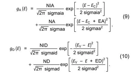
The total intrinsic density is shown as NID for donor traps and NIA for acceptor traps. Total density is denoted as ND for the donor and NA for the acceptor. The difference between intrinsic and doping energy is EA and ED, EA for acceptor trap and ED for donor traps. Sigmaia is the width of Gaussian distribution of intrinsic acceptor traps. Similarly, Sigmaa is thewidth of Gaussian distribution of the dopant for acceptor traps. Sigmaid and sigmad are the same for donor traps.Here, parameters for captured cross-sections charge are also defined. Sigae defines the capture cross-section of the electron for acceptor traps. Sigah defines the capture cross-section of the hole for acceptor traps. Similarly, Sigde and sigdh are related to donor traps. For P3HT device modelling the values are shown below.
3.5. Hopping mobility model
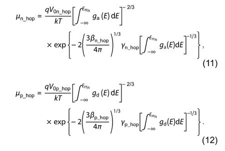
The hopping mobility model is based on charge generation and recombination. Here μn_hopand μp_hopis the effective mobility of electrons and holes. The Eq. (11) is related to electrons. Here V0n_hopis frequency of attempts to jump an electron in the conduction band and ga(E) is the density of state (DOS) for the acceptor-like conduction band. βn_hopis percolation constant, γn_hopis 1/carrier localization radius. Similarly, in Eq. (12) subscript p stands for holes and all these parameters corresponding to previous description and gd(E) is the density of state (DOS) for the donor-like valance band.
3.6. Poole-Frenkel mobility model
The Poole-Frenkel mobility model depends on charge movement. It is described by Eqs. (13) and (14).
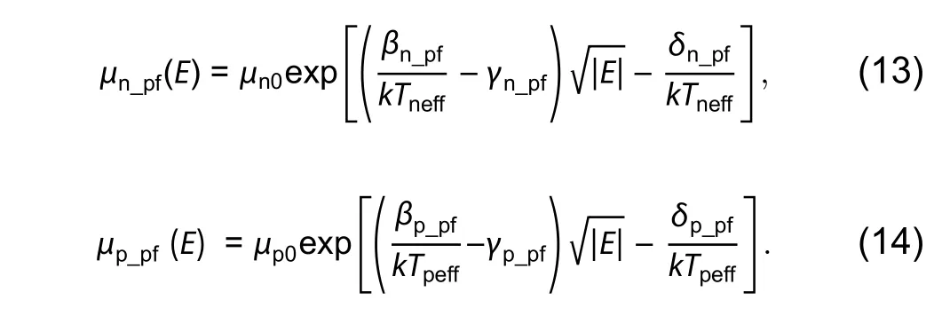
In these equations effective mobility of negative and positive charges is μn_pfand μp_pf, respectively. Here μn0is the zero field electron mobility, μp0is the zero field hole mobility,δp_pf, δn_pfare activation energy for holes and electrons. βn_pfand βp_pfdenote the Poole-Frenkel factor for electron and hole, respectively. Net effective temperatures are TpeffandTnefffor holes and electrons respectively. In this modelling interface charge (Qf) between insulator and semiconductor is essential to describe the characteristics of device. It also describes the recombination velocity at the interface surface.
In this modeling we use two different mobility models so the net resultant mobility is
4. Result and discussions
Fig. 2(a) shows the UV-Vis absorption spectra of the P3HT thin film coated on the cleaned glass substrate. The high absorption peak at the 458 nm wavelength corresponds to π-π*transition. The absorption spectra also display absorption bands at 613 nm which correspond to π-π stacking, similar to our previously reported paper[34,35]. The (αhυ)2versus hυ plot has been shown in the inset of the Fig. 2(a)from which the band gap of the P3HT has been estimated to be Eg= 1.9 eV. The surface morphology of polymer thin film is a very important parameter for studing and understanding the charge transport. We performed the study of the surface morphology of P3HT dissolved in chloroform and coated on the SiO2/Si substrate using AFM in tapping mode. The AFM image of P3HT thin film shows the large numbers of tiny crystallites as shown in Fig. 2(b). The fabricated OTFT has a bottomgate bottom-contacts structure as shown in Fig. 1 which is similar to the structure as in Ref. [18]. A 50 nm thick P3HT layer is employed for 50 μm channel on 300 nm SiO2dielectric. A 30 nm thick Au electrode work as the source and drain terminal.The length of contacts is 2 mm. A heavily doped n+Si act as the gate terminal. The width of the device is 2 mm. We created the similar structure as shown in Fig. 1 using ATLASTMcommercial device simulator for numerical simulation of the device using the above reported TCAD model for P3HT based OTFTs.

Fig. 3. The transfer (I DS-VGS) characteristics of P3HT-based bottomgate bottom-contact (BGBT) OTFTs. Solid lines show TCAD simulation and symbols show experimentally measured results.
4.1. Discussion on density of state
During the simulation, we have observed the effects of parameters. Here we present the observation with respect to absolute values of all input-output variables. NTD affect the threshold voltage, when it increases, the absolute value of drain current decreases and off region of OTFT increases.WTD also shows the same impact but it also depends on the range of NTD. Now about NTA, it affects the curvature of current output graph but up to a certain limit. Increasing the value of this variable bends the graph but after a critical value, the drain current becomes zero or about to zero. The effect of WTA is also similar but WTA also depends on NTA.Thus the tail distributions of DOS is observed. Despite these,it is also observed that donor parameters play a more effective role than the acceptor parameter. Now we discuss deep distributions. NGD affect the drain current graph at the lower and middle region of the gate voltage. When we increase the value of NGD the drain current of specified region decreases.EGD and WGD show similar effects on drain current graph but partially dependent on NGD. At another side, NGA directly affects the leakage current of the device. When the value of NGA increases, the leakage current also increases. Similarly, EGA and WGA also affect the leakage current but these are partially depended on NGA. Here one more point is noticeable, that captured cross-section charge variables (i.e. sigtae,sigtah, etc.) control the current through the traps. Therefore,the effect of other DOS parameters also increases at higher values of these variables. Because of the increase of the total traps in the cross section area, the drain current increases.
4.2. Discussion on double peak density of state (DOS)
It is observed that single peak distribution of DOS could not fit the model of OTFT. So a double-peak distribution is essential for describing the characteristic of the device. NIA and NA describe the curve of output current graph but not as sharp as the single-peak DOS parameter. NID and ND affect the off region of the device. It controls the point where the current starts to flow, also known as threshold voltage. Similar with single peak DOS, the captured cross-section of charge affects the resultant drain current and the other DOS parameter. As this is double peak distribution, the effects of these parameters show their effect in large region of output current graph.
4.3. Discussion on mobility models
In organic semiconductors (OSCs) two types of charge transport mechanism are there, localized and delocalized.The hopping transport is localized and band transport is delocalized transport. The mobility model is initially developed for the inorganic crystalline semiconductor. After rigorous research on OSCs, some other models are also developed for OSCs i.e. multiple trapping and release (MTR), Pool-Frenkel,and remote phonon scattering. In this work, Pool-Frenkel and hopping mobility model are considered. The Pool-Frenkel mobility model has six parameters for the electron and hole. In the simulation, it is observed that hole parameters affect the output most and electron parameters do not affect the output as much. When δp_pfdecreases 10-2to 10-5, drain current increases. When βp_pfdecreases 10-5to 10-11, drain current decreases. This model strongly depends on electric field.So it shows a convergence problem many times. For double peak DOS it is essential to define hopping mobility model.
4.4. Verification and parameter extraction
The electrical characterization of the considered device has been performed and we got the experimental data from the measured transfer and output characteristics of the fabricated device. Here we have also simulated the electrical behaviour of this device. The transfer (IDS-VGS) characteristic was extracted at 4 points of drain voltage, these were -15, -30, -45,-60 V voltages for both the cases ie in measurement as well as in TCAD simulation. The gate voltage was swept from +20 to -0 V by the step of 1 V. The comparison of the transfer(IDS-VGS) characteristics obtained from the TCAD simulation and experimental measurement are shown in Fig. 3.
In this OTFT leakage current is about 2 nA. The dielectric thickness influences the leakage current. In this OTFT dielectric thickness is greater than usual so leakage is higher. The gate leakage current also depends on traps and flows in opposite direction to the main IDScurrent.
The output (IDS-VDS) characteristic was also extracted like this for both cases, i.e. in measurement as well as in TCAD simulation. The gate voltage was fixed at six points +10, 0, -10,-20, -30, -40 V voltages. The drain voltage was swept from 0 to -60 V by step of 1 V. The comparison of the measured and simulated output characteristics (IDS-VDS) is shown in Fig. 4.The maximum drain current depends on charge carrier doping concentration. When doping concentration increases the drain current also increases. Mobility of holes and electrons also affect the output drain current. The resultant mobility of charges, which is calculated by mobility model, plays a key role in device performance. The device structure and W/L also affect the device characteristic. Increase in width of OTFT increases the charge transport while an increase in length of channel decreases the charge transport.
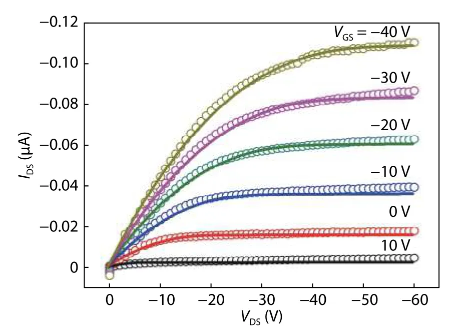
Fig. 4. (Color online) The output (I DS-VDS) characteristics of P3HTbased bottom-gate bottom-contact (BGBT) OTFTs. Solid lines showing TCAD simulation and symbols showing experimentally measured results.
About the performance parameter, usually seven parameters describe the performance, which is shown in Table 6.Here COXis gate capacitance per unit area. It depends on the dielectric constant of the insulator and its thickness.

The threshold voltage defines the voltage point where the majorly currents start to flow. The formulas for drain currents are as, Eq. (16) is for linear region and Eq. (17) for saturation region
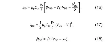
So Eq. (17) can be written as Eq. (18) and here according standard notation,is slope and VTis intersecting point on x-axis[19]. The ( IDS)1/2-VGScharacteristics of OTFT is shown in Fig. 5, from which threshold voltage is calculated from the plot ofvs VGSvalues and best fit a line to the curve and extrapolate it on x-axis. Thus, we get intersect point as VT=14 V. The sub-threshold slope defines the control of drain current through gate voltage. It shows minimum gate voltage value to change one-decade drain current. It is calculated as an inverse of maximum slope of logIDvs VGcurve[20].
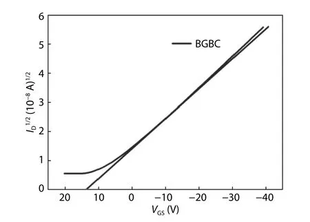
Fig. 5. The ( I DS)1/2-VGS characteristics of OTFT.
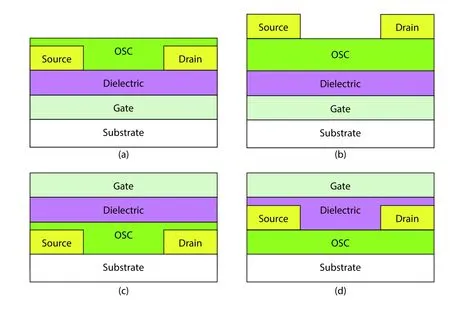
Fig. 6. (Color online) Different structure configurations of OTFT. (a) Bottom-gate bottom-contact. (b) Bottom-gate top-contact. (c) Top-gate bottom-contact. (d) Top-gate top-contact.

Transconductance is the effect of gate voltage on drain current. According to its definition, it represents an effect on output of input voltage. So it can also be estimated by the first derivative of ID-VGplot[21].

Now Eq. (16) can be written as a standard liner equation with slope ‘m’ and intersect on y-axis as ‘c’.

So by a graphical method slope it can be calculated by first derivative of IDSvs VGSgraph and it is equal to m. The slope is already calculated as Gm. So

The carrier mobility in linear region is calculated as Eq.(18), it is also used by Swati Singh et al.[21].

Thus, carrier mobility in the saturation region is also calculated from Eq. (17), (18) and with help of slope extraction.

So carrier mobility in the saturation region is calculated as Eq. (26)[20]. The results are tabulated in Table 6. Now,about Ion/Ioffratio, this is maximum to minimum current ratio.It represents switching capability. It depends on leakage current and maximum drive current. The higher ratio is good for transistor, but in sensors, it also depends on sensitivity of device and material. All calculated values are compared in the table below.
5. Comparison of various structures of P3HTbased OTFTs
The semiconductor is the core of the transistor. In different structures, the OSC layer interacts with other material layers and these phenomena affect the charge injunction as well as the charge transport. When a metal layer deposits on the organic semiconductor layer, during the interaction some charge transfer occurs to align the Fermi levels of semiconductor and metal. These charge combination create a potential barrier at the interface. It is known as the Schottky barrier. The charge transportation across the barriers affects the resulted drain current. Therefore, performance of different structures varies. The interaction of the organic semiconductor with substrate material also affects the charge transport. So this effect differentiates the performance of top gated device to bottom gated device. To observe these theoretical effects on OTFT we decide to simulate other structures also. The previous model is successfully examined with experimented data of P3HT-based BGBC OTFTs. To observe the effects of structures on output characteristic, three additional structures are also simulated, i.e. bottom-gate top-contact (BGTC), top-gate bottom-contact (TGBG) and top-gate top-contact (TGTC). These structures are shown in Fig. 6. The comparison of performance parameter is tabulated in Table 7. All the dimensions of structure are the same only the sequence of the layers is changed.

Table 7. Performance parameters comparison of four structures of P3HT-based OTFT.
The selection of geometry depends on required application. The BGTC has good metal-semiconductor interface so it exhibits high performance. Generally, it is used for research to analyse the characteristic of new materials. On the other hand, BGBC structure is more suitable for practical applications. It has lower device performance but it is suitable for fab-rication. TGBC is feasible solution for large area printing.
5.1. Discussion on output characteristics
The developed model is used to simulate structures and I-V characteristics ie IDS-VGSand IDS-VDScharacteristics of the OTFTs in all four configurations. From the I-V characteristic of the OTFTs the performance parameters of the OTFTs are calculated and compared.
5.1.1. Bottom gate bottom contact (BGBC)
The I-V characteristic of BGBC structure is shown in Fig. 7. As previously discussed, BGBC has lower performance.So in output characteristics, it can be easily observed that BGBC has the lowest drain current among the various configurations. It implies, that the structure is feasible for sensors, displays and biodegradable circuits. During this simulation it is observed that in BGBC structure, the drain current exponentially increases at high voltage. The saturation level is missing till the high voltage level. In the IDS-VGSplot, it is observed that the mobility of charge carrier in the high voltage region is higher than lower voltage.
5.1.2. Bottom gate top contact (BGTC)
Fig. 8 shows the I-V characteristics of BGTC structure.The BGTC structure has better carrier injection. The characteristics imply that it has higher charge carrier mobility. In this graph the maximum drain current is almost double than BGBC. The simulation shows that the structure has lower leakage current and better on-off ratio. In this structure, the OSC layer deposits on smooth surface of dielectric layer. On the other hand, bottom contact structure has staggered the OSC layer that decreases interface charges between contacts and the semiconductor. Therefore, the top-contact device performs better than the bottom-contact device.
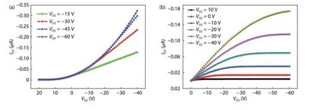
Fig. 7. (Color online) I-V characteristic of BGBC structure. (a) Transfer characteristics. (b) Output characteristics.

Fig. 8. (Color online) I-V characteristic of BGTC structure. (a) Transfer characteristics. (b) Output characteristics.

Fig. 9. (Color online) I-V characteristic of TGBC structure. (a) Transfer characteristics. (b) Output characteristics.
5.1.3. Top gate bottom contact (TGBC)
Fig. 9 shows the I-V characteristics of TGBC structure.The main difference in this structure is that OSC layer interacts with substrate layer. So the number of traps increases and it affect the charge carriers contributing in charge transport. Thus, the charge mobility is higher than the bottomgated device. The traps affect drain current positively. In IDS-VGSgraph, it can easily be observed that drain current slowly saturates. The maximum drain current is much higher than bottom gate structures. The mobility is also highly affected due to traps. All the properties signify that this structure is suitable for printing.
5.1.4. Top gate top contact (TGTC)
Fig. 10 shows the I-V characteristics of TGTC structure. In this structure, the OSC and substrate interacts in large area.So in this case the number of traps increases and it affect the charge carriers available for charge transport. The OSC is also placed on one plane rather than staggered. The contacts also inject more charge for charge transport. Therefore, we are able to get more drain current in the TGTC structure as compared to the other structures and the output is better than TGBC. But it has greater leakage current than BGTC so the on-off current ratio is less than BGTC. The mobility in this structure is also the highest. The saturation region is also sharp due to increased traps. This structure is better for switching applications.

Fig. 10. (Color online) I-V characteristic of TGTC structure. (a) Transfer characteristics. (b) Output characteristics.
After simulation, it is observed that among these four structures top-contact structures shows higher drain current.The performance is varying due to metal-OSC interface layer resistance. The second cause is increment in traps between OSC and substrate. This justifies that layer design affects the performance of OTFTs and channel formation is also affected by structure configuration.
5.2. Discussion on performance parameter
The performance parameters describe its characteristics on some scale. Here six parameters are extracted and compared in Table 7. The BGTC structure has the best on-off ratio. The threshold is nearby each other. The charge carrier response is the highest in TGTC, it can be estimated by mobility. The sub-threshold voltage also defines the minimum voltage required to change the drain current to 10 times. So TGTC also has a good response ratio. The leakage current of TGTC is an issue for lagging in performance of the TGTC structure. It can be considered as a future work to minimize leakage current.
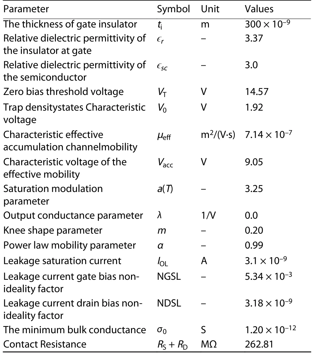
Table 8. Compact model parameters extracted for P3HT-based OTFT.
6. Compact modeling, model parameter extraction & compact model verification
6.1. Compact modeling
To address the various physical phenomenon of the OTFT device, the compact modelling is needed to understand in a wider form with respect to all OTFT devices by incorporating device physics and their operation by defining various device parameters such as charge carrier (holes in our case) accumulation mode, the exponential density of states (DOS),parasitic resistance caused due to non-linearity, source/drain contacts without junction isolation, dependence of mobility on electric field (E) and temperature (T)[20,28-39]. Since the OTFT device is mainly operated in the accumulation region, a unique and robust model i.e., universal organic TFT (UOTFT)model with the accurate implementation of UCCM[20]has been used in this work to validate our experimental results due to various key features of this model[28-32]for which the equivalent circuit is given in Fig. 11.

Fig. 11. Equivalent circuit of UOTFT model[31, 38].
The charge accumulation in n-channel OTFT per unit area at zero-channel potential (-Qacc)ois calculated by the help of solution of the UCCM equation[28-32]given by the following equations.
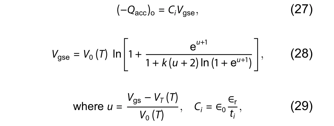
where symbols have their usual meaning and more information can be found in Refs. [31, 32]. P-channel OTFT equations can be obtained by direct change in voltage, charge polarity and current.
6.1.1. Effective channel mobility
According to the results of percolation theory[28-33], effective channel mobility is expressed in the UOTFT model as:

where symbols have their usual meaning and more information can be found in Ref. [31]. The power-law dependence of the mobility on carrier concentration is defined by the temperature-dependent model parameter α.
6.1.2. Intrinsic drain-source current
Drain-source current of intrinsic transistor due to charge carriers accumulated in the channel is defined by general interpolation expressions[28-32,39]

The effective channel conductance in the linear region Gchis obtained in the following way:

The drain saturation current Isatis determined by the following formula:

where Vsatis the saturation voltage obtained as:

with a being the temperature dependent model parameter,where symbols have their usual meaning and more information can be found in Refs. [31, 33]. The total intrinsic drain to source current is given by following:

where Idsis total current andis accumulated current andis leakage current given by[31,32]

where IOLis the temperature-dependent leakage saturation current model parameter, NDSL and NGSL are the drain and gate bias non-ideality factors, respectively, σ0is the model parameter representing the zero bias drain source sheet conductivity and Vthis the thermal voltage at device operating temperature.
6.2. Comparison of experimental characteristic and compact model-based simulated characteristics
In this section we compared the OTFT compact modelling results with the experimental results. Fig. 12(a) shows the comparison of transfer characteristics obtained from experimentally measured data & compact model based simulated characteristic of P3HT-based BGBC OTFT. The transfer characteristics are obtained by varying the gate to source voltage(VGS) from 20 to -60 V keeping drain voltage constant at -15,-30, -45, and -60 V.
Fig. 12(b) shows the output characteristics obtained from experimentally measured data and compact model based simulated characteristic of P3HT based BGBC OTFT. Output characteristics is obtained by varying the drain to source voltage(VDS) from 0 to -60 V keeping gate to source voltage (VGS) constant at 20, 10, 0, -10, -20, -30, and -40 V. There is very good agreement between experimentally measured and compact model based simulated transfer and output characteristic of P3HT-based BGBC OTFTs.

Fig. 12. (Color online) (a) Comparisons of transfer characteristics of the experimentally measured data with the compact model-based simulated data. (b) Comparisons of output characteristics of the experimentally measured data with the compact model-based simulated data.Symbols show experimentally measured data and solid line show compact model-based simulated data.
6.3. Parameter extraction
Extracted OTFT model parameters for P3HT based bottom-gate bottom-contact (BGBC) OTFTs using the UOTFT model are given in Table 8. The extraction process starts with the collection of data for IDS-VGSand IDS-VDScharacteristic and providing it in the UTMOST I-V data base in.uds format. Further simulation of IDS-VDSand IDS-VGScharacteristic using the above mentioned compact model and optimization of this characteristic using Levenberg Marquardt optimization technique with respect to experimental data for extraction of model parameters have been performed. Extracted model parameters are listed in Table 8.
6.4. Simulation of logic circuit
The current state of art with respect to organic logic circuit design and implementation is quite challenging in manufacturing point of view, a different n-type material as well as p-type material-based OTFT having different threshold voltage of complementary MOS technology[36,37], which is not desirable. Therefore, a different n- and p-type material based complementary logic circuits are still tough to make a place in commercial market. Although a unipolar-based inverter has their own pros and cons. In this paper we have intended to make a modest attempt to realize a practical logic inverter circuit. We applied the above discussed compact model for simple logic circuit simulation based on p-channel P3HT-based OTFTs only. The p-channel zero gate source load(ZGSL) configuration-based inverter circuit[36-38]has been designed and studied as a part of the compact model validation as shown in Fig. 13(a) which is used for simulation of voltage transfer characteristics (VTC plot) and transient characteristics of the inverter. We choose a unipolar configuration having similar threshold voltage and fixed the channel length of both load and driver OTFT. In the steady state the load current (IDL) and driver current ( IDD) are equal. In this circuit top p-channel OTFT (W = 1000 μm, L = 50 μm) with W/L ratio 1000/50 acts as load transistor and bottom p-channel OTFT acts as driver. In the given inverter circuit the load OTFT is always in on condition and depending on the input at driver OTFT it switches between the ON and OFF condition. When the input voltage is lower than the threshold voltage (more positive than VT), the driver OTFT turns off. On the other side,when it is more than the threshold voltage (more negative than VT), the driver OTFT turns on. The operation of the inverter also depends on load TFT size relatively with the driver TFT. Fig. 13(b) shows the voltage transfer characteristics (VTC)plot of the inverter circuit under consideration for W/L ratio of 1, 2, 4, 6, 8 and 10 of driver TFT. As the W/L ratio of the driver OTFT increases, its impedance decreases and the transition between high and low states becomes clearer.
When the load OTFT is in saturation (ON) condition, the drain current

When input voltage (Vin) is zero [for ‘p’ type-high logic state], the driver OTFT will be ‘OFF’ and load current is equal to zero. Therefore, using Eq. (39) when ∣IDL∣=0, the above expression changes as

When the Vinis -100 V [Low state], the driver is in the saturation state, the drain current is passed into the ground and therefore, ∣Vout∣≅0V. The low and high logic states used in logic circuit simulation based on P3HT based OTFTs are given in Table 9.

Table 9. Low and high logic states used in logic circuit simulation based on P3HT based OTFTs.
When we entered into ‘low’ state to ‘high’ state, thedriver OTFT will be go from saturation to deep linear region and gradually it will become less and less conductive, and when it reached to the high state, the driver transistor will be‘OFF’. When the driver goes into the linear regime, (i.e., close to the lower state), sharp fall will be observed. When the driver circuit is in deep triode region (close to high state region), as Voutgradually increases, again the gain will decrease.The transition inverter gain increases as higher the W/L of driver OTFT which can also be seen from simulations obtained from UOTFT model as shown in Fig. 13(b). In conclusion, ZGSL configuration provided, higher logic swing and higher will be the gain along with improvement of noise margin of the inverter.

Fig. 13. (a) A circuit diagram of the inverter circuit used for assessing the simulation results. (b) Voltage transfer characteristics of the inverter circuit shown for different W/L ratios of driver OTFT. (c) Transient characteristics of the inverter with driver OTFT has W = 100 μm and L = 50 μm and load OTFT has W = 1000 μm and L = 50 μm.

Fig. 14. (a) Circuit diagram of the three stage ring oscillator circuits. (b)Ring oscillator output waveform.
When ∣ Vout∣≥∣Vin∣-∣VTp∣, the driver transistor in saturation regime, the drain current is expressed as

When the driver OTFT goes into linear regime
In steadystate, ∣IDD∣ = ∣ IDL∣ and relationship between input and output voltage can be obtained using load and driver circuit operational regime. Fig. 13(c) shows the transient response of the inverter with driver OTFT has W = 100 μm and L = 50 μm and load OTFT has W = 1000 μm and L =50 μm.
We also simulated a three stage ring oscillator circuit with the help of extracted compact model parameters and basic inverter circuit discussed above. The three stage ring oscillator circuit is shown in Fig. 14(a) and simulated output waveform is shown in Fig. 14(b). Thus we successfully demonstrated the application of universal organic thin film transistor compact model in design and simulation of p-channel OTFT based inverter and 3 stage ring oscillator circuit which supports that the compact model is suitable for circuit simulation in order to take care of future needs of organic TFT based integrated circuits.
7. Conclusion
In this paper we presented a TCAD-based model of P3HT-based OTFT using the ATLAS simulator which is validated against experimental data for P3HT based BGBC OTFTs.It includes double peak, tail and deep states of density of states (DOS) for traps to describe the I-V characteristic in both sub threshold and above threshold region of the OTFT.It included Pool-Frenkel and hopping mobility models. Understanding the charge transport with physical phenomenon is useful for optimizing the process of fabrication and device performance. After validation of the TCAD model we simulated three other configurations of the structures, i.e. BGTC, TGBC and TGTC OTFTs and compared them on the basis of six performance parameters of OTFTs. Further we also present compact modeling and model parameter extraction of the P3HTbased OTFT. Compact model has been applied for circuit simulation of p-channel P3HT OTFT-based inverter circuit for simulating its voltage transfer characteristics (VTC plot) and transient characteristics. Compact model performs well for these logic circuit simulations. Also we successfully simulated three stage ring oscillator circuit using the extracted OTFT compact model parameters. It shows that the compact model is suitable for circuit simulation in order to take care of the needs of the future organic TFT based Integrated Circuits.
Acknowledgements
This work is funded by SERB, DST Government of India.The authors are thankful to SERB, DST Government of India for the financial support under Early Career Research Award(ECRA) for Project No. ECR/2017/000179. Mr Shubham Dadhich is thankful for Receiving Junior Research Fellowship (JRF)under this project.
 Journal of Semiconductors2021年7期
- Journal of Semiconductors的其它文章
- Blue perovskite LEDs
- ~1.2 V open-circuit voltage from organic solar cells
- Engineering microstructures for efficient Sb2(Sx Se1-x)3 solar cells
- Post-sulphuration enhances the performance of a lactone polymer donor
- Suppressed light-induced phase transition of CsPbBr2I:Strategies, progress and applications in the photovoltaic field
- Efficient MAPbI3 solar cells made via drop-coating at room temperature
