Renaissance of tin halide perovskite solar cells
Shurong Wang , Aili Wang , Feng Hao , and Liming Ding
1School of Materials and Energy, University of Electronic Science and Technology of China, Chengdu 611731, China
2Center for Excellence in Nanoscience (CAS), Key Laboratory of Nanosystem and Hierarchical Fabrication (CAS), National Center for Nanoscience and Technology, Beijing 100190, China
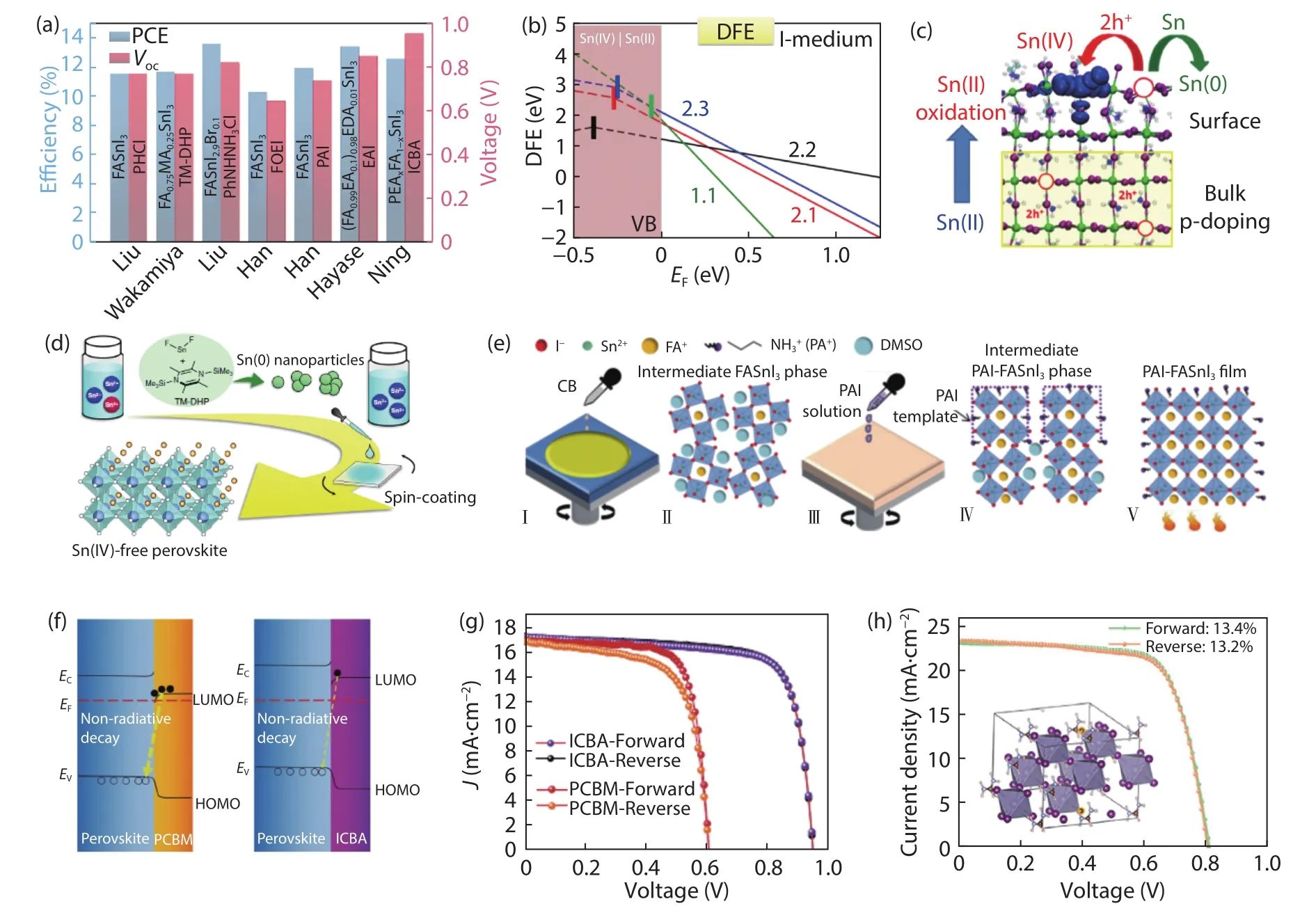
Halide perovskite solar cells (PSCs) have attracted wide interests in photovoltaics field due to the prominent advantages of perovskite materials.To date, the certified power conversion efficiency (PCE) of lead-based PSCs has reached to 25.5%[1].However, the toxicity of lead in PSCs limits the practical application.Tin (Sn)-based perovskites are the most promising candidates because of their narrow bandgap and comparable optoelectronic properties to lead analogues.The relatively narrower bandgap of Sn-perovskites possess expanded absorption of sunlight.The pioneering Sn-based PSCs based on MASnI3(MA = methylammonium) gave 5%–6% PCEs[2].Notably, the inferior device performance and stability restrict the explorations due to the facile oxidation of Sn2+to Sn4+, fast crystallization, low formation energy of Sn vacancies and high level of self-doping[3,4].Currently, efforts are devoted to the development of reducing reagents, manipulation of the perovskite dimensionality, and optimization of the interfacial energy level alignment of Sn-based PSCs.As summarized in Fig.1(a), the PCE of Sn-based PSCs break double digits recently, indicating a renaissance of the Pb-free PSCs exploration.Here, the most recent advances of Sn-based PSCs are highlighted.
To probe the defect chemistry of Sn-perovskites, the lattice instability and electronic disorder act as triggers for unfavorable oxidation from Sn2+to Sn4+[5].Besides, the calculation of defect formation energy (Figs.1(b) and 1(c)) indicated that Sn2+was only stable within the bandgap of bulk and Sn4+defects usually located in the deep valence band (VB)[6].The oxidation to Sn4+could be activated at the surface acting as a surface electron trap (Fig.1(c)).Therefore, the Sn4+elevates the defect concentration and exacerbates carrier recombination, leading to a deterioration of device performance, especially the open-circuit voltage (Voc).
To suppress the oxidation of Sn2+, various reducing additives such as hypophosphorous acid[7], Sn(0) powder[8], and hydrazine vapor[9]were utilized.Liuet al.introduced phenylhydrazine hydrochloride (PHCl) into FASnI3(FA = formamidinium) perovskite films to reduce the existing Sn4+since PHCl has a reductive hydrazine group and a hydrophobic phenyl group[10].The resulting PSC gave a PCE of 11.4%.Meanwhile,the unencapsulated device showed almost no decay in a glovebox for over 110 days.Suppressed oxidation of Sn2+could effectively inhibit the carrier recombination, leading to long carrier lifetime and accessibleVoc.Wakamiyaet al.used 1,4-bis(trimethylsilyl)-2,3,5,6-tetramethyl-1,4-dihydropyrazine (TM-DHP)to react with SnF2to form Sn(0) nanoparticles (Fig.1(d))[8].The formed Sn(0) nanoparticles in the precursor solution could scavenge Sn4+, thus enabling strong photoluminescence and prolonged decay of the deposited perovskite films.The PCE of resulting device increased to 11.5%, with aVocof 0.76 V.Most recently, Liuet al.introduced phenylhydrazine cation (PhNHNH3+) to improve the illumination stability of FASnI3[11].Therefore, the use of efficacious reducing additives gifts the Sn-PSCs with high performance and stability.
Particularly, the relatively fast crystallization of Sn-perovskite films with unfavorable defects and rough morphology poses a great challenge for achieving high PCE and stability for Sn-based PSCs.In this regard, Hanet al.precisely controlled the crystallization process by reducing the surface energy with pentafluorophen-oxyethylammonium iodide(FOEI)[12].This approach enabled highly oriented and smooth FASnI3films with lower defect density and longer carrier lifetime.The resulting PSCs offered a certified PCE of 10.16%.The crystallization process was further regulated with n-propylammonium iodide (PAI)[14].PAI could induce templated growth of FASnI3crystals by forming the intermediate phase(Fig.1(e)), thus resulting in a highly crystallized FASnI3film with preferential orientation along (100) plane and reduced trap density.Finally, a stabilized PCE of 11.22% was achieved and the device kept over 95% of its initial efficiency after 1000 h operation at the maximum power point (MPP).These results indicate that the retarded grain growth promotes forming high-quality and oriented Sn-perovskite films.
Moreover, large organic cation (ethylenediammonium,EA+; phenylethylammonium, PEA+) were used to regulate the composition and structure of Sn-perovskites.The substitution of A-site cations with ethylenediammonium and guanidinium cations was proved to cause lattice strain relaxation of Sn-perovskites[15,16].Hayaseet al.reported the correlation between lattice strain relaxation and the PCE of Sn-based PSCs.Substituting the A-site cations with smaller cations could reduce the lattice distortion, leading to improved carrier mobility and higher photovoltaic performance[17].Hanet al.also did mixed-cation engineering to stabilize the perovskite phase in a tin triplehalide amorphous layer with CsFASnI3polycrystals[18].This special structure could block the moisture, oxygen and ion diffusion in the devices.A certified PCE over 10% was achieved and over 95% of the initial PCE was retained after working at MPP for 1000 h.Hayaseet al.incorporated large EA+cation into MASnI3abiding by the Goldschmidt tolerance factor to make vertically-oriented 2D/3D mixed perovskite films[19].The resulting PSCs gave aPCE of 9.24% and 95% of the initial efficiency was retained after being kept in a glovebox for 30 days without encapsulation.

Fig.1.(Color online) (a) Representative PCE and Voc for Sn-based PSCs in 2020.Labels in the bar chart indicate perovskite components and additives (ICBA as ETL).(b) Defect formation energy diagram for bulk Sn(IV) defects in MASnI3 perovskites.(c) Schematic illustration of Sn2+ oxidation to Sn4+.Bulk Sn4+ transforms to Sn2+, releasing two holes to the valence band (VB) and p-doping the perovskite, while surface Sn4+ acts as a deep electron trap.Reproduced with permission[6], Copyright 2020, American Chemical Society.(d) Schematic illustration of the Sn4+-scavenging method with TM-DHP.Reproduced with permission[8], Copyright 2020, Springer Nature.(e) Fabrication and crystallization of Sn-based films with PAI treatment.Reproduced with permission[14], Copyright 2020, Royal Society of Chemistry.(f) The diagram for recombination at perovskite-ETL interface.(g) J–V curves for Sn-based devices with ICBA or PC61BM as ETL.Reproduced with permission[13], Copyright 2020, Springer Nature.(h) J–V curves for Sn-based devices with PhNHNH3Cl treatment.Reproduced with permission[11], Copyright 2020, Elsevier.
Regarding the bandgap (1.35 eV) of Sn-based perovskites, reducing the voltage loss is a key challenge for getting high PCE for Sn-based PSCs.Good energy level alignment at interface affords effective electron extraction from perovskites to the electron-transport layer (ETL).Ninget al.introduced ICBA (indene-C60) as ETL to replace PC61BM ([6,6]-phenyl-C61-butyric acid methyl ester) and improvedVocto 0.94 V (Figs.1(f) and 1(g))[13].The shallower lowest unoccupied molecular orbital (LUMO) energy level of ICBA brought thisVocgain.Meanwhile, suppressing the interfacial carrier recombination between Sn-based perovskites and ETL can increaseVoc.Interestingly, the surface Fermi level of Sn-based perovskites with EAI shifted to shallower value, thus effectively passivating Sn4+traps/defects[20,21].Liuet al.slightly substituted I–with Br–to form FASnI2.9Br0.1to realize better energy level alignment with C60[11].Br–doping results in a larger lattice shrinkage and a slight increase of bandgap, in comparison to pure iodide perovskite[11].Owing to the strongs–pandp–pcouplings[22], the VB shifted downwards realizing an optimal energy level alignment between Sn-perovskites and ETL.The resulting device gave a PCE of 13.4% (certified 12.4%) with long-term durability, also setting a new PCE record for Sn-based PSCs (Fig.1(h)).
In summary, the advances and recent renaissance of Snbased PSCs are highlighted.The urgent challenge is to improveVoc.Adjusting the composition and structure of perovskites with large organic cations, reducing crystal defects and charge carrier recombination, and selecting suitable ETLs for good energy level alignment are very crucial in enhancing the performance of Sn-based PSCs.
Acknowledgements
This work was supported by the National Natural Science Foundation of China (51702038), the Sichuan Science &Technology Program (2020YFG0061) and the Recruitment Program for Young Professionals.L.Ding thanks the National Key Research and Development Program of China(2017YFA0206600) and the National Natural Science Foundation of China (51773045, 21772030, 51922032, 21961160720)for financial support.
 Journal of Semiconductors2021年3期
- Journal of Semiconductors的其它文章
- White light-emitting diodes from perovskites
- Adjusting energy level alignment between HTL and CsPbI2Br to improve solar cell efficiency
- Blade-coated organic solar cells from non-halogenated solvent offer 17% efficiency
- Self-assembled monolayers enhance the performance of oxide thin-film transistors
- I ndium–gallium–zinc–oxide thin-film transistors: Materials,devices, and applications
- L ow-dimensional materials for photovoltaic application
