Interfacial properties of g-C3N4/TiO2 heterostructures studied by DFT calculations*
Chen-Shan Peng(彭春山), Yong-Dong Zhou(周永东), Sui-Shuan Zhang(张虽栓), and Zong-Yan Zhao(赵宗彦),†
1Faculty of Materials Science and Engineering,Kunming University of Science and Technology,Kunming 650093,China
2Department of Architectural Engineering,Henan Quality Polytechnic,Pingdingshan 467000,China
Keywords: photocatalysis,g-C3N4,TiO2,heterostructures,interfacial states
1. Introduction
Since Wang et al. reported the photocatalytic hydrogen production of g-C3N4,[1]the g-C3N4has received extensive attention from researchers due to its excellent performance.For example, g-C3N4has the advantages of reasonable electronic band structure (band gap 2.70 eV), non-toxicity, low cost, long-term stability, and convenient preparation.[2–8]Although its photocatalytic activity has been confirmed in previous research, most of the reported photocatalytic efficiencies of the pure g-C3N4are limited by the high recombination rate of its photo-generated electron–hole pairs.[9–11]Accordingly, it has become an important research direction to explore high-efficiency g-C3N4-based photocatalysts with better separation/transfer efficiency of photo-generated electron–hole pairs. In order to solve this problem, many attempts have been made to improve its photocatalytic properties,such as non-metal doping,[12,13]metal doping,[14,15]noble metal loading,[16]heterostructure constructing,[17]etc.Among these methods,the heterostructures coupled with another photocatalyst can reduce the recombination rate of the photo-generated electron–hole pairs,and many kinds of photocatalysts,such as TiO2, WO3, ZnO, etc.,[18–22]have been adopted to construct the g-C3N4-based heterostructures.
In the latest development of g-C3N4-based photocatalysts, the TiO2-constructed heterostructure has become a research hotspot due to its feasibility and effectiveness for the spatial separation of photo-generated electron–hole pairs. The TiO2is the most popular photocatalyst and combining TiO2with other semiconductors to build heterojunction has several obvious advantages in enhancing the electron–hole pair separation.[23,24]Therefore, the g-C3N4/TiO2heterostructure has been extensively studied to further enhance the visible light catalytic activity.[25–27]Different kinds of g-C3N4/TiO2composite photocatalysts with heterostructure have been prepared by various strategies in previous studies. For instance,g-C3N4/TiO2nanocomposites were successfully prepared by a solid-state method through using urea and commercial TiO2as precursors, showing that the absorption and photocatalytic properties in visible-light region are enhanced.[28]Ren et al.synthesized the g-C3N4/TiO2heterojunction by in situ synthesis, which showed good photodegradation towards Orange II.[29]Liu et al.[30]and Tan et al.[31]used a one-step method to synthesize a hetero-structured g-C3N4/TiO2composite,which can rapidly degrade pollutants with visible-light irradiated.[30,31]
Although many experimental researches indicated that the g-C3N4/TiO2heterostructure can enhance photocatalytic performance, the corresponding intrinsic and essential mechanism has rarely been explained in depth.[32–34]In this paper, the supercell models for g-C3N4/TiO2heterostructure formed by monolayer g-C3N4and TiO2(001)surface are constructed at first. The structural and electronic properties of these models are further calculated by density functional theory(DFT).Based on these results,the underlying mechanism of g-C3N4/TiO2heterostructure to enhance the photocatalytic performance is proposed.
2. Computational methods and models
All calculations in the present work were performed through the Cambridge Serial Total Energy Package (short as CASTEP) codes.[35]The core electrons were treated by the ultrasoft pseudopotential;[36]and the exchange–correlation functional in the generalized gradient approximation (GGA)was described by using the PBE.[37]In order to accurately describe the nonbonding van der Waals interaction along the caxis, the DFT-D of van der Waals dispersion corrections was used.[38]In the present work,a“fine”quality setting was used to achieve a good compromise between speed and accuracy,which is suitable for most of calculations. The Monkhorst–Pack scheme K-points grid sampling was set to be 1×1×1 for the irreducible Brillouin zone. A 54×32×256 mesh was used for fast Fourier transformation. An energy cutoff of 340 eV was used for expanding the Kohn–Sham wave functions. The minimization algorithm chosen was the Broyden–Fletcher–Goldfarb–Shanno scheme.[39]The convergence criteria for optimizing all model geometric structures were set to be 1×10⁻⁶eV per atom for the self-consistent field tolerance,0.03 eV·˚A-1for the maximum force, 0.05 GPa for the maximum stress tolerance,1×10-3˚A for the maximum displacement tolerance,1×10-5eV per atom for the maximal energy change. Then, the optimized structures were further used to investigate the electronic structures and other properties.
For the construction of heterostructure,an important factor is crystal lattice matching. An ideal heterostructure requires the lattice constants of the two components to match with each other as much as possible. If the crystal lattice mismatch is too large, the interface is unstable due to the large interfacial stress. Consequently, in the present work, in the case of g-C3N4/TiO2–H heterostructure(“H”refers to g-C3N4combined horizontally with TiO2as shown in Fig. 1(a)), a four-layer TiO2(001) slab was chosen as a substrate with a 3×2 supercell (11.35 ˚A×7.57 ˚A). This supercell can match well with a 1×1 unit cell of g-C3N4(12.35 ˚A×7.13 ˚A).The degree of mismatching crystal lattice is u=8.44% and Δv=5.99%. If the lattice mismatch at the interface is less than 10%,then such an interface is considered to be capable of forming composite materials with heterostructure. More importantly, for two-dimensional material (i.e., g-C3N4) loaded on the surface of three-dimensional material(i.e.,g-TiO2),the interface stress generated by lattice mismatch can be further released through the deformation of two-dimensional material along the normal direction of the interface (i.e., [001] direction). Therefore, the lattice mismatch mentioned above can be accepted for the experimental feasibility. In the case of g-C3N4/TiO2–V heterostructure(“V”denotes g-C3N4combined vertically with TiO2), two different kinds of models were considered: g-C3N4/TiO–VC and g-C3N4/TiO–VN.Between them,the interface of g-C3N4/TiO2–VC heterostructure has C atoms of g-C3N4as the contact point as shown in Fig. 2(a),while the interface of g-C3N4/TiO–VN heterostructure has N atoms of g-C3N4as the contact point as shown in Fig.3(a).For all models,the atoms in the two first layers that are close to the interface are allowed to be freely relaxed, while the atoms in the other two layers that are on the other side of the slab are fixed to mimic the bulk effect. To eliminate the interaction between two neighboring images along the normal direction,the thickness of vacuum layer was set to be 20 ˚A.
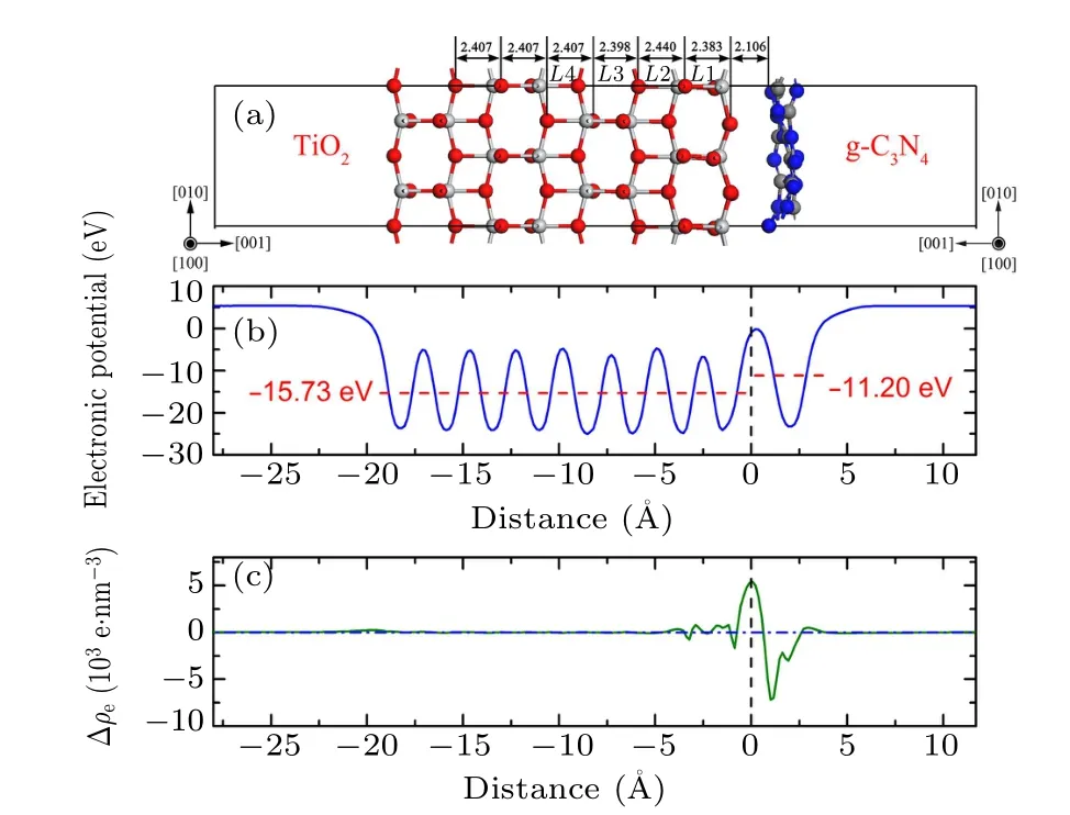
Fig.1.(a)Side view of g-C3N4/TiO2–H interface model,(b)average electrostatic potential,and(c)difference in average electron density along interfacial normal direction.
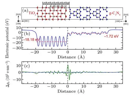
Fig.2. (a)Side view of g-C3N4/TiO2–VC interface model,(b)average electrostatic potential,and(c)difference in average electron density along interfacial normal direction.
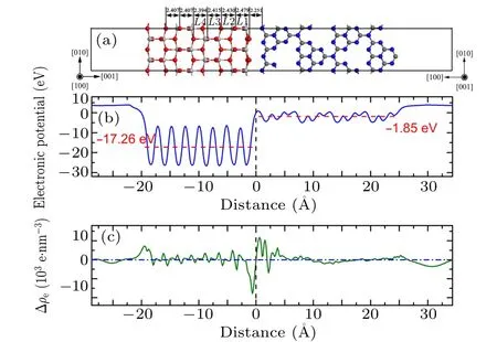
Fig.3. (a)Side view of g-C3N4/TiO2–VN interface model,(b)average electrostatic potential, (c) difference in average electron density along interfacial normal direction.
3. Results and discussion
3.1. Interfacial structures and interfacial energy
To investigate the stabilities of g-C3N4/TiO2heterostructures,the structural parameters including interface formation energy, interface spacing, and lay spacing expansion are calculated and the results are listed in Table 1. The interface spacing of the g-C3N4/TiO2–H heterostructure is 2.106 ˚A;the interface spacing of the g-C3N4/TiO2–VC heterostructure is 1.945 ˚A; the interface spacing of the g-C3N4/TiO2–VN heterostructure is 2.251 ˚A. The interfacial spacing of the g-C3N4/TiO2–VC heterostructure is found to be minimal,which is closely related to the interface atomic composition. For example, when g-C3N4contacts the TiO2in a vertical manner,since g-C3N4contacts the TiO2, C atoms, and N atoms, respectively, at the interface, there is a difference in interface spacing or interface energy. Therefore, the interface spacing of g-C3N4/TiO2–VC heterostructure is smaller than that of g-C3N4/TiO2–VN heterostructure. At the same time, the interfacial spacing of g-C3N4/TiO2–H heterostructure is found to be between the interfacial spacing of g-C3N4/TiO2–VC heterostructure and that of g-C3N4/TiO2–VN heterostructure.This is caused by the formation of different bonds when the interfaces interact,because the g-C3N4/TiO2–H heterostructure interface bonds are mainly van der Waals bonds. The layer spacing expansion represents the local relaxation: positive value denotes widened spacing.Comparing these three heterostructures, the first atomic TiO2layer in the g-C3N4/TiO2–H heterostructure is inward relaxed, while the first atomic TiO2layer in the g-C3N4/TiO2–VC heterostructure and the g-C3N4/TiO2–VN heterostructure are outward relaxed. The value of layer spacing gradually decreases from L1 to L3,approaching to the value of bulk spacing. These different phenomena indicate that the g-C3N4has different effects on the substrate when placed in different ways to construct the heterostructure.

Table 1. Calculated interfacial parameters of relaxed heterostructures: interface spacing, expansion of lay spacing, and interface formation energy(γint)in units of meV/˚A2.
The stability and realizability of interfaces are usually evaluated by the interface formation energy (γint). In the present work,the interface formation energy is calculated from the following formula:

in which ETiO2-surface, Eg-C3N4, and Eg-C3N4/TiO2-interfaceare the total energy of the models of TiO2surface,g-C3N4molecular layer, and g-C3N4/TiO2interface; S is the area of the interface. The interface formation energy of g-C3N4/TiO2–H heterostructure is smallest, and its value is 3.967 meV/˚A2,which is obviously smaller than those of other two vertical heterostructures (6.518 meV/˚A2for g-C3N4/TiO2–VC, and 7.943 meV/˚A2for g-C3N4/TiO2–VC).The interface formation energy of g-C3N4/TiO2–VC heterostructure is very large,implying the strong interaction between g-C3N4and TiO2. The strong interface formation can represent strong interface interaction, and vice versa. By combining the calculation results of interfacial spacing,the g-C3N4/TiO2–VC heterostructure can be determined to have a tight interface, while the g-C3N4/TiO2–H heterostructure possesses a van der Waals weak interface.
3.2. Electronic structures
To investigate the underlying mechanism of the high activity of g-C3N4/TiO2composite photocatalyst, the local and partial densities of states of g-C3N4/TiO2interfaces were calculated and depicted in Figs. 4–6. When g-C3N4and TiO2are combined to form a g-C3N4/TiO2–H heterostructure, the Fermi level(EF)is relatively shifted in the forbidden band,indicating the variation of the band alignment in different kinds of the g-C3N4/TiO2interfaces. The N-2p,N-2s, Ti-3d, C-2p,and O-2p states contribute considerably to the top of valence band(VB),in which the contribution of N-2p states and O-2p states are predominant. The bottom of VB is mainly composed of the C-2p and N-2p states. The bottom of conduction band (CB) is made up of C-2p, N-2p, Ti-3d, and O-2p states, and has a slightly hybridized state, in which the Ti-3d state is dominant. The density of states of the g-C3N4/TiO2–VC and g-C3N4/TiO2–VN interfaces are identical to that of g-C3N4/TiO2–H interface. However, the top of CB split into many peaks, implying that more obvious delocalization phenomena occur. At the same time, it is observed that the g-C3N4/TiO2–VC and g-C3N4/TiO2–VN interfaces produce obvious interface states that are caused by N-2p and C-2p state in the forbidden band.The interface state of g-C3N4/TiO2–VC interface is most obvious,which presents outstanding metallic properties. Combined with the analysis of interface formation energy and interface spacing in the previous section,the interfacial spacing of g-C3N4/TiO2–VC heterostructures is shown to be minimal. That is to say, the interface state appearing in the forbidden band presents metallic properties and contributes to the transfer of photo-generated electrons and holes, which can effectively improve the photocatalytic performance of g-C3N4/TiO2heterostructure.
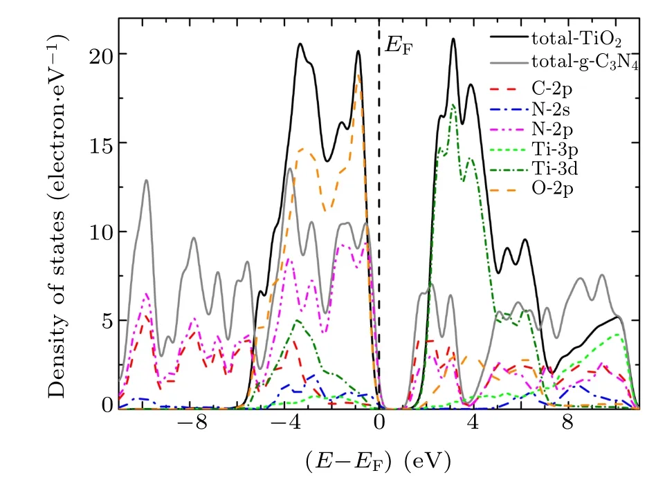
Fig.4. Local and partial densities of states for g-C3N4/TiO2–H heterostructure at interface.
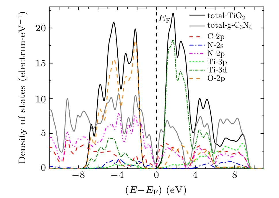
Fig. 5. Local and partial densities of states for g-C3N4/TiO2–VC heterostructure at interface.
To investigate the charge transfer and separation at the interface,the Mulliken population analysis of the plane-wave pseudopotential calculation is performed on the three heterostructures and is the results are depicted in Fig.7. In order to compare the monolayer g-C3N4with the bulk of TiO2,the results of the Mulliken charge are also calculated in which the C and N atom have a Mulliken charge of 0.480 e and-0.380 e,respectively. The Ti and O atoms have a Mulliken charge of 1.330 e and-0.670 e, respectively. From Fig.7(a), it can be found that the O atom has a Mulliken charge of-0.660 e and-0.620 e at the interface of the g-C3N4/TiO2–H heterostructure, compared with that of TiO2bulk, the change of the O atom is not very obvious. At the interface,the number of Mulliken charges for the Ti atom is 1.350 e,which is slightly larger than that of the TiO2bulk phase of 1.330 e. In general, the change in the number of Mulliken charges carried by the O and Ti atoms in the TiO2layer near the interface is not significant as compared with that in the TiO2bulk. For g-C3N4,the number of Mulliken charges for the C atom at the interface is 0.450 e,and the number of Mulliken charges for the N atom is-0.390 e and-0.410 e,which means that the C atom loses very few electrons,compared with that of monolayer g-C3N4,while the N atom gains electrons. It is indicated that a slight charge transfer occurs along the direction from g-C3N4to TiO2at the interface.
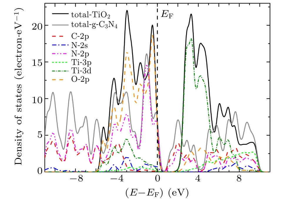
Fig.6.Local and partial densities of states for g-C3N4/TiO2–VN heterostructure at interface.
For the g-C3N4/TiO2–VC heterostructure as shown in Fig.7(b),the Mulliken charge number of the O atom and the Ti atom in the TiO2layer at the interface are-0.660 e(-0.640 e)and 1.320 e, respectively. This is in contrast to the values of the bulk phase of TiO2(-0.670 e and 1.330 e),where both the Ti and O atom lose some electrons. At the interface,the number of Mulliken charges for the C atom in the g-C3N4layer is 0.390 e, which indicates that the C atom is electron-accepted compared with the g-C3N4bulk phase (0.480 e) and N atom loses electrons.It is shown that a slight transfer of charge from the TiO2layer to the g-C3N4layer occurs at the interface. For the g-C3N4/TiO2–VN heterostructure as shown in Fig. 7(c),the O atom in the TiO2layer loses electrons, the N atom in the g-C3N4layer gains electrons, and the electron transfer at the interface is the same as that for the g-C3N4/TiO2–VC heterostructure.
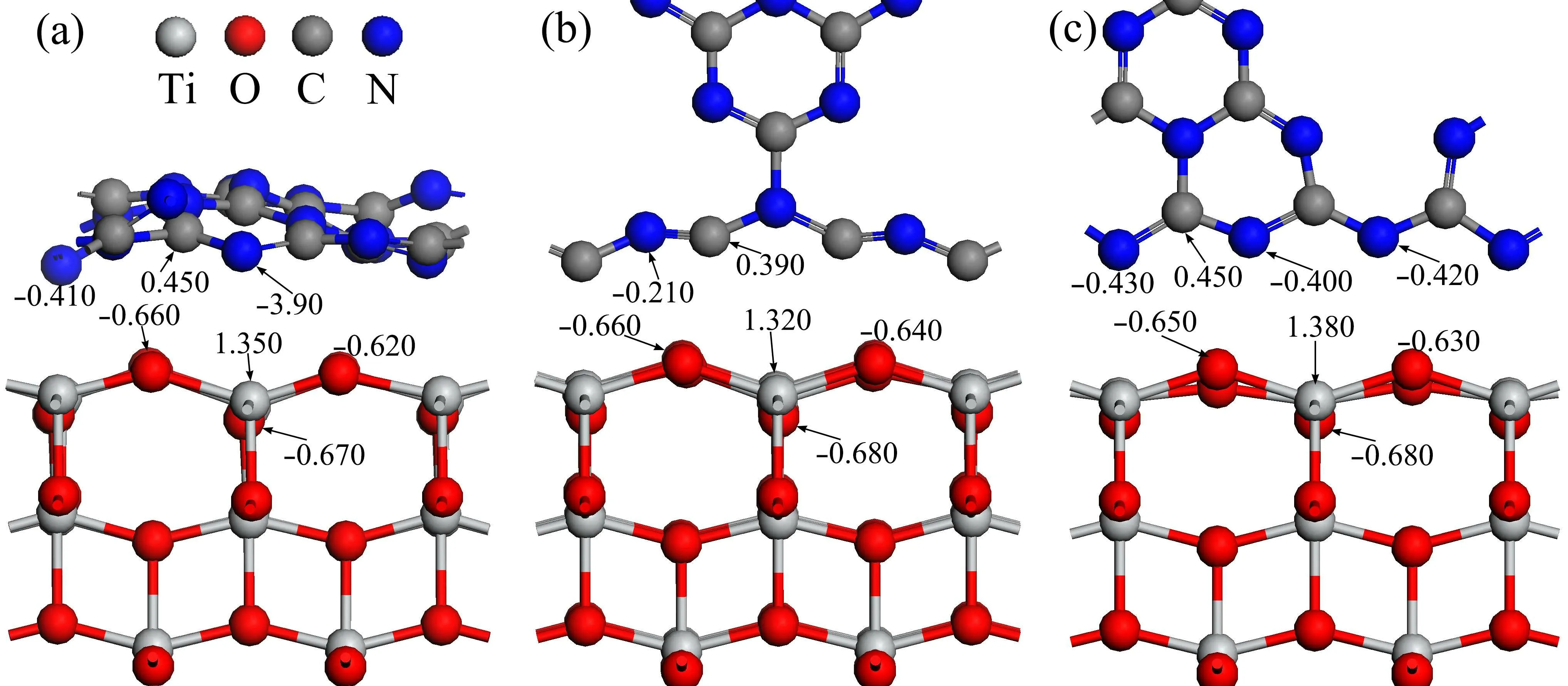
Fig.7. Mulliken population analysis of(a)g-C3N4/TiO2–H heterostructure,(b)g-C3N4/TiO2–VC heterostructure,and(c)g-C3N4/TiO2–VN heterostructure.
3.3. Built-in electric fields
The calculated electronic potential and planar-averaged charge density difference along the normal direction of the interface are depicted in Figs.1–3. For the g-C3N4/TiO2–H heterostructure, as shown in Fig. 1(b), the average potential of TiO2is -15.73 eV, which is significantly lower than that of g-C3N4(-11.20 eV).At the interface,the electronic potential has a mutation along the normal direction of the interface due to the crystal lattices of the atoms arranged on both sides being not consistent. In addition, the relaxation of the position of the interface atoms causes the arrangement of atoms in the interface to be different from that of the lattice lattices on both sides. Therefore,the electrostatic potential in the interface region is also different from the potential distribution on both sides. It is found that there is a significant mutation in the average electrostatic potential at the interface,and an interfacial electric field is formed in a narrow interval, and the direction of the electric field is directed from TiO2to g-C3N4. Under the action of the electric field, the carriers are each drifted in the direction of the applied electric field force. This is advantageous for improving photocatalytic performance. As shown in Fig.1(c),it is found that the electron density of the g-C3N4at the interface decreases, and the charge density in the TiO2layer increases, which indicates that there is a charge transfer along the direction from g-C3N4to TiO2. This result is consistent with the analysis of the Mulliken population above.In other words,a dipole moment is generated at the interface.That is to say, the generation of the dipole moment at the interface creates a built-in electric field, which is advantageous for improving the separation efficiency of carriers at the interface and suppressing the recombination of photo-generated electron–hole pairs.Moreover,the situation that the charge depletion and accumulation mainly occur between the TiO2slab and the g-C3N4slab also demonstrates that the interaction between TiO2and g-C3N4is very weak, which means that the g-C3N4/TiO2–H possesses a vdW heterostructure.
The electrostatic potential along the interfacial normal direction of g-C3N4/TiO2–VC heterostructure is illustrated in Fig. 2(b). The obvious feature is that the potential of TiO2layer (with an average potential of -18.8 eV) is lower than that of g-C3N4layer(with an average potential of-1.72 eV).When the g-C3N4and TiO2contact each other and form a vertical hetero-structure,at the interface,the average electrostatic potential has a very obvious mutation,and a strong interfacial electric field is formed in a narrow interval,which contributes to the separation of electrons and holes.The difference in average electron density along the normal direction of the interface is shown in Fig. 2(c). It is found that the accumulation layer of electrons is formed on the TiO2side,and a depletion layer is formed on the g-C3N4side at the interface. This indicates that a small quantity of charge transfer from the TiO2layer to the g-C3N4layer at the interface,which is consistent with the result of the Mulliken population analysis above.
For the g-C3N4/TiO2–VN heterostructure as shown in Figs. 3(b) and 3(c), the accumulation region of charge at the interface is close to the g-C3N4layer and some peaks appear,and the charge dispersion region is close to the TiO2layer,which is the opposite to the scenario for g-C3N4/TiO2–VC.This shows that this has a weakening effect on the built-in electric field produced at the interface. However, the situation of the potential in the normal direction along the interface is the same as that of the g-C3N4/TiO2–VC heterostructure. A dipole moment is generated at the interface, and the built-in electric field thus caused contributes to enhancing photocatalytic performance.
Based on the above analysis, in the cases of g-C3N4/TiO2–H and g-C3N4/TiO2–VC heterostructures, the electrons accumulate in the center of interfacial region,while in the case of g-C3N4/TiO2–VN heterostructure,the electrons accumulate on the side of g-C3N4layer. The electrons’transfer and accumulation will generate an additional electric field.In the former two cases, these additional electric fields can weaken the interfacial built-in electric field, which is generated by the lattice potential. In summary, the built-in interfacial electric field is directed from TiO2(001)layer to g-C3N4layer.Moreover,the additional electric field produced by electron transfer in the case of g-C3N4/TiO2–VN heterostructure will obviously enhance this electric field. On the other hand,the calculated results of electronic structures indicate that the photo-generated electrons will be transferred from the CB of g-C3N4layer to the CB of TiO2layer, which is consistent with recent experimental observations.[40–44]Thus,the photogenerated electron transfer process will be accelerated under the action of interfacial electric field. Therefore, the forming of the interface between g-C3N4and TiO2is conducive to the separation of photo-generated electron–hole pairs,and the improvement of the performance of g-C3N4and TiO2composite photocatalyst,which is found in recent experiments.[40–44]
4. Conclusions
Three kinds of g-C3N4/TiO2heterstructures are considered and compared in the present work. When g-C3N4combines horizontally with TiO2to form a heterostructure, they are combined through van der Waals interaction. The spacing between two layers is larger and the interface formation energy is smaller. Although there is an electric field built into the interface between the two components, it is difficult to transfer electrons between them due to the large spatial hindrance. However, the interfacial van der Waals interaction can regulate the electronic structure on both sides of the interface, so that the photocatalytic reaction can be carried out independently on both sides of the interface, which can promote the improvement of photocatalytic performance. When g-C3N4combines vertically with TiO2to form a heterostructure through C atoms, they have strong covalent interaction.The spacing between two layers is smaller and the interface formation energy is larger. There is a built-in electric field between the two components,and the atoms are bonded to each other, making it very easy for electrons to transport between them. At the same time,the interfacial interaction can further regulate the electronic structure on both sides,so that the photocatalytic reaction can be carried out independently on both sides of the interface,which can significantly enhance the photocatalytic performance. The latter g-C3N4/TiO2heterostructure is relatively difficult to synthesize in experiment,but it is worth trying. These findings provide some helpful guidances in developing the g-C3N4/TiO2heterostructure-based photocatalysts.
- Chinese Physics B的其它文章
- Two-dimensional finite element mesh generation algorithm for electromagnetic field calculation*
- Stable water droplets on composite structures formed by embedded water into fully hydroxylated β-cristobalite silica*
- Surface active agents stabilize nanodroplets and enhance haze formation*
- Synchronization mechanism of clapping rhythms in mutual interacting individuals*
- Theoretical study of the hyperfine interaction constants,Land´e g-factors,and electric quadrupole moments for the low-lying states of the 61Niq+(q=11,12,14,and 15)ions*
- Ultrafast photoionization of ions and molecules by orthogonally polarized intense laser pulses: Effects of the time delay*

