
Integrated 3D Fan-out Package of RF Microsystem and Antenna for 5G Communications
2020-10-26 08:21
ZTE Communications 2020年3期
(The 58th Research Institute of China Electronics Technology Group Corporation,Wuxi 214000,China)
Abstract: A 3D fan-out packaging method for the integration of 5G communication RF mi⁃crosystem and antenna is studied.First of all,through the double-sided wiring technology on the glass wafer,the fabrication of 5G antenna array is realized.Then the low power devices such as through silicon via (TSV) transfer chips,filters and antenna tuners are flip-welded on the glass wafer,and the glass wafer is reformed into a wafer permanently bonded with glass and resin by the injection molding process with resin material.Finally,the thinning resin surface leaks out of the TSV transfer chip,the rewiring is carried out on the resin sur⁃face,and then the power amplifier,low-noise amplifier,power management and other devic⁃es are flip-welded on the resin wafer surface.A ball grid array (BGA) is implanted to form the final package.The loss of the RF transmission line is measured by using the RF millime⁃ter wave probe table.The results show that the RF transmission loss from the chip end to the antenna end in the fan-out package is very small,and it is only 0.26 dB/mm when working in 60 GHz.A slot coupling antenna is designed on the glass wafer.The antenna can operate at 60 GHz and the maximum gain can reach 6 dB within the working bandwidth.This dem⁃onstration successfully provides a feasible solution for the 3D fan-out integration of RF mi⁃crosystem and antenna in 5G communications.
Keywords: AiP;fan⁃out package;RF microsystem;3D integration;5G communications
1 Introduction
Owing to the growing operating frequency up to hun⁃dreds of gigahertz,minimized size and power con⁃sumption,as well as the requirement of better perfor⁃mance of RF system,the novel communication and sensing applications such as 5G and automotive applications are urged to integrate every section part of RF system chain,so as to establish the“everything in one”module with minisize and multi-functions.As the wave length of microwave shrinks with the growing of its frequency,the characteristical⁃ly electrical length of antennas and transmitting lines can be reduced to millimeter or even micron level,which calls for higher fabrication accuracy of interconnection process.Be⁃sides,packaging process with heterogeneous integration abili⁃ty offers an opportunity for novel package architecture with chips of different materials and fab features[1].The antenna-inpackage (AiP) based on wafer level fabrication process can fabricate tremendous modules simultaneously with semicon⁃ductor process,which offers compact and low cost solution and paves a possible way for RF modules with high perfor⁃mance and low cost[2].
In order to meet the needs of 5G miniaturized communica⁃tion systems,new packaging technologies in the millimeter wave frequency range are needed to solve the basic technical challenges of millimeter wave,such as low loss and ultra wide⁃band interconnection,high wiring density,thin packaging sub⁃strate,high performance integrated passive devices (IPD) and reducing shape factors[3].Dozens of papers are reported on AiP and its applications[4].The cutting edge system corporations and outsourced semiconductor assembly and tests (OSATs)have offered numbers of AiP solutions,many of which are based on wafer level fan-out (WLFO) process,and the sub⁃strate options focus on silicon,organic compound,glass and more[5–6].The glass substrate with low epsilon and coefficient of thermal expansion(CTE)is an ideal choice for high frequen⁃cy application,and the compound substrate allows process flows with low price and agile combination,which is conve⁃nient for heterogeneous integration[7–8].By combing glass and compound substrates in AiP module,the advantages of perfor⁃mance and cost can be taken together.The encapsulated an⁃tenna in 60 GHz band is a research hotspot.The traditional printed circuit board (PCB) technology is very convenient to realize multi-layer structure and antenna array[9].The low tem⁃perature co-fired ceramic(LTCC)technology has the advantag⁃es of light and thin structure,many wiring layers and narrow line width,but its lamination temperature is higher than 850 ℃,which is much higher than that of destroying active de⁃vices.Therefore,although it is possible to create sealed multi⁃layer substrates with integrated passive components and anten⁃nas,active devices must be packaged and connected separate⁃ly because of the high temperature process of LTCC[10–11].
A 3D fan-out integrated packaging method for 5G communi⁃cations RF microsystem and antenna is presented in this pa⁃per.Based on a new 3D fan-out wafer-level packaging archi⁃tecture,the permanent bonding process of glass wafer and res⁃in reconstructed wafer is designed.Based on glass and resin composite materials,the high density integrated interconnec⁃tion of heterogeneous chip and antenna array is realized.Fi⁃nally,the process manufacturing of antenna and packaging module is completed,and the high quality 5G communications AiP module manufacturing is realized.It can provide 64 an⁃tenna channels and 7 RF chips.The volume is only 18 mm ×18 mm × 1 mm,which can meet the application requirements of miniaturized 5G communications equipment.
2 Measurement of Transmission Loss
In order to obtain the RF transmission performance of the 3D fan-out integrated package,a planar coplanar waveguide(CPW) transmission line and a 3D stacked CPW transmission structure are fabricated.Because the connection between the RF microsystem and the antenna usually uses CPW,it is very important to obtain the RF transmission loss of CPW[12].The CPW transmission line is realized by redistribution layer(RDL) process in 3D fan-out wafer level packaging.The struc⁃ture of CPW transmission line is distributed on both sides of the signal line,so it is very suitable for millimeter wave probe station,and more convenient for testing.The structure of CPW is shown in Fig.1.

▲Figure 1.Structure of coplanar waveguide(CPW).

▲Figure 2.Coplanar waveguide(CPW)with 3 different lengths.
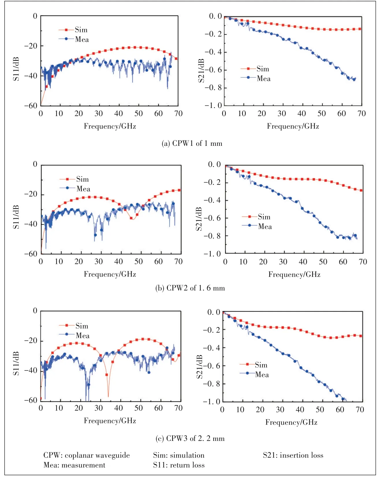
▲Figure 3.Comparison of test and simulation results of CPW.
Firstly,the CPW transmission line structure is fabricated on the glass wafer.The picture of the CPW transmission line is shown in Fig.2.The dielectric constant of the glass wafer is 6.3 and the dielectric loss tangent is 0.01,and the thickness of the glass substrate is 300 μm.The transmission line is made of copper and is 5 μm thick.The surface of the transmis⁃sion line is covered with a 10 μm thick poly⁃imide to protect the copper wiring layer from ox⁃idation.The width of the CPW transmission line is 70 μm and the spacing is 25 μm.CPW trans⁃mission lines with lengths of 1.00 mm,1.60 mm and 2.20 mm are fabricated respectively.A rect⁃angular test window of 100 μm × 300 μm is opened in the polyimide layer at both ends of the transmission line.
The transmission line is measured on a high frequency probe test bench,using a groundsignal-ground (GSG) probe with a distance of 100 μm and a phasor network analyzer (PNA)network analyzer for 67 GHz performance.The test results are shown in Fig.3,and it can be found that the radio frequency transmission loss of the CPW transmission line on the glass wafer is very small.It can be seen from the figure that there are some differences between the test re⁃sults and the simulation results.This is because wafer manufacturers can only give the dielec⁃tric constant and loss tangent angle of glass be⁃low 5 GHz,which makes the simulation results in the high frequency part above 5 GHz inaccu⁃rate.In addition,the test joint of the high frequen⁃cy probe table will also lead to part of the inser⁃tion loss.
The transmission loss of CPW working in 60 GHz is calculated.When the CPW trans⁃mission line works in 60 GHz,the insertion loss is 0.26 dB/mm,as shown in Table 1,where the RF transmission loss of glass wafers is very small,and it is a good choice for 3D fan-out integration of RF microsystems and antennas.
Then the glass-based CPW transmission line is packaged through the fan-out type to form a fan-out package to simulate the fan-out package structure of the RF chip.Solder balls are planted at the leading end of the package and flip-flopped on the glass-based CPW substrate to test a completed transmis⁃sion link from the chip end to the package.The photos of the process structure and processing are shown in Fig.4.Fig.5 shows the complete signal path,and the processing size of the stack interconnected package is 5 mm×6 mm×0.92 mm.
The 3D stacked transmission structure is finally measured in the high-frequency probe table,and the test results are shown in Fig.6.It can be seen that the RF transmission loss of the 3D stacked CPW transmission structure is very small,which indicates that the 3D fan-out package structure will not bring about too much loss.Fig.6 shows that there are some dif⁃ferences between the test results and the simulation results.This is because the wafer manufacturer cannot give the materi⁃al electrical parameters in the high frequency stage,whichwill affect the simulation results in the high frequency band.But the test results are basically consistent with the simulation results,which shows that the early simulation has a certain guiding significance.
▼Table 1.CPW transmission loss operating in 60 GHz
3 Design and Measurement of AiP
▲Figure 4.3D stacked coplanar waveguide (CPW) transfer structure and photos.

▲Figure 5.Transmission path of the RF signal through the package.
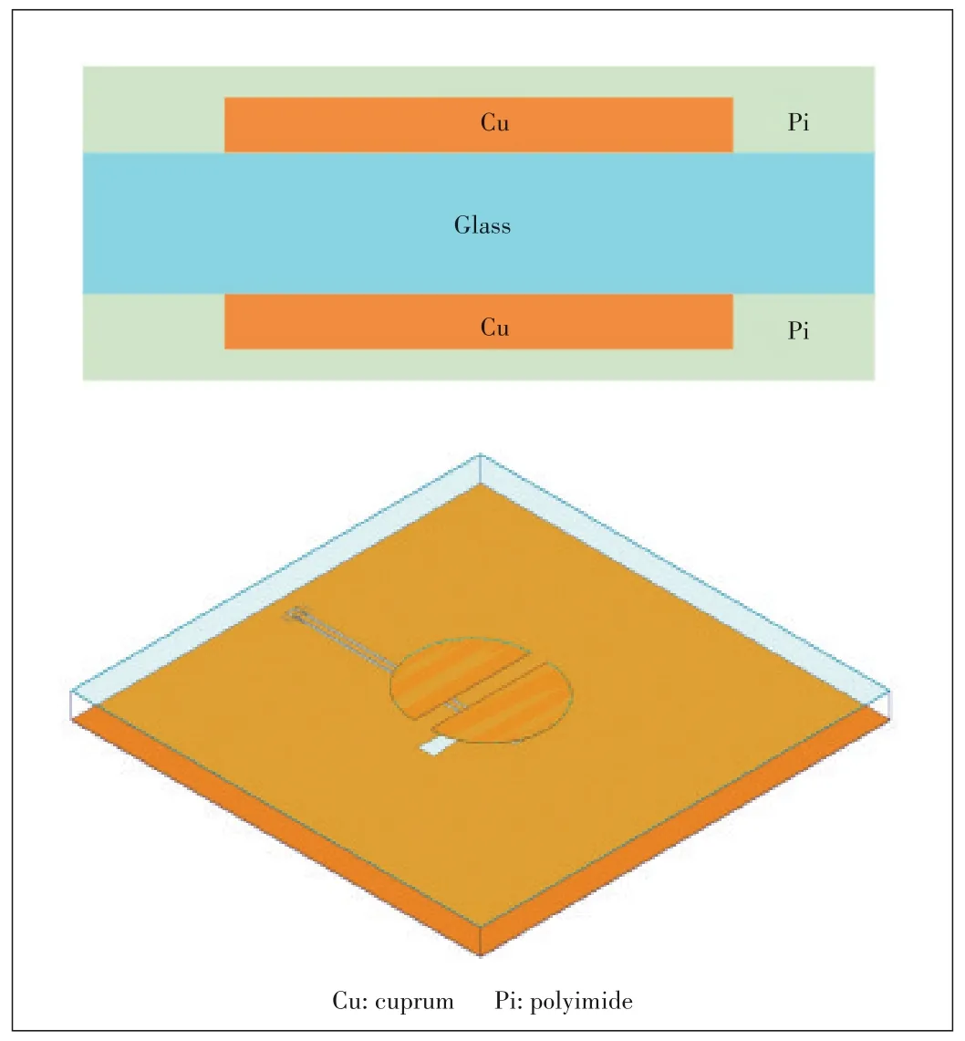
The patch antenna is very suitable for wafer-level process⁃ing[13].The wiring process is carried out on the positive and negative sides of the glass wafer(300 μm thick,dielectric con⁃stant is 6.3,and dielectric loss tangent is 0.01) to form a slot coupling antenna.The glass wafer is used as the radiation patch of the antenna,and the radiation patch is realized by two semicircular patches.The back of the wafer is used as the feed and reflection ground plane of the antenna,and the cou⁃pling gap is located directly below the radiation patch,which is used to stimulate the radiation patch.The patch antenna is fed by CPW with terminal open circuit and slot coupling,and the size of CPW is adjusted to make its characteristic imped⁃ance 50 Ω,and the function of the coupling gap is to excite the whole patch without an additional gap coupling layer,which makes it easier to integrate with the circuit.It is pre⁃cisely because of the existence of the coupling gap that the current which originally flows along both sides of the CPW gap on the floor will flow along the edge of the coupling gap,so that the electromagnetic coupling between the CPW and the radiation patch is enhanced.Fig.7 is a structural diagram of the slot coupling antenna.

▲Figure 6.Comparison between test and simulation results of 3D stacking coplanar waveguide(CPW).
The electromagnetic simulation software high frequency structure simulator (HFSS) is used to simulate and optimize the slot coupling antenna.After analysis and optimization,the size of the antenna element is 5 mm×5 mm,the diameter of the two semicircular radiation patches is 1.43 mm,the gap of the two semicircular radiation patches isg=0.196 mm,and the size of the feeder and coupling gap isW=2.8 mm,W1=0.2 mm,L1=0.07 mm,L2=0.615 mm,g1=0.025 mm.Fig.8 shows the spe⁃cific structure of the antenna.
▲Figure 7.Antenna structure and geometry.
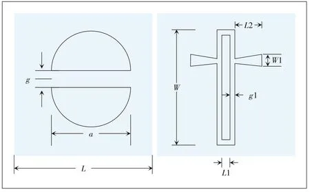
▲Figure 8.Specific structure of the antenna.
The slot coupling antenna is fabricated by wiring the front and back sides of the glass wafer.First,the radiation surface of the antenna with 5 μm thick copper is made on the front of the glass wafer,and then it is protected with 10 μm thick poly⁃imide.The CPW feeder and coupling gap are made on the back of the glass wafer,also protected by polyimide,and a rectangular test port is opened on the polyimide layer to leak the copper CPW transmission line.
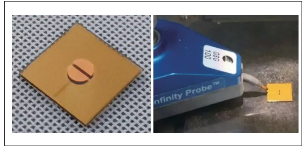
The structure of the antenna is measured by the high frequen⁃cy probe table.Fig.9 shows the slot coupled antenna photos and test photos.From the measurement results,it can be found that the working frequency of the antenna whose reflection coef⁃ficient is less than -10 dB is 56.2–63.8 GHz.The difference between the simulation results and the measurement results is mainly attributed to the deviation of the process in the manu⁃facturing process,but the antenna still has the working band⁃width of 7 GHz,which meets the design requirements very well.Fig.10 shows the emission coefficient of the antenna.
Fig.11 shows the radiation pattern of the antenna.We can see that the radiation direction of the antenna is directly above the radiation patch,which is very suitable for the stacking in⁃tegration of RF microsystem and antenna.The top of the 3D stack integration is used for the manufacture of transceiver an⁃tennas and the bottom is used for the integration of RF chips.
▲Figure 9.Slot coupled antenna photo and test photo.

▲Figure 10.Reflection coefficient of antenna.

▲Figure 11.Radiation pattern of antenna.
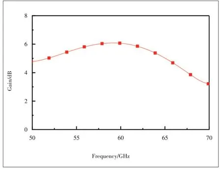
The gain of the antenna is higher than 5.5 dB in the whole working bandwidth and has the maximum gain of 6 dB in 59.8 GHz.And it has a good directionality.Fig.12 shows the simulation results of antenna gain in the working bandwidth.
4 Integration of RF Microsystem and An⁃tenna
4.1 Architecture of AiP
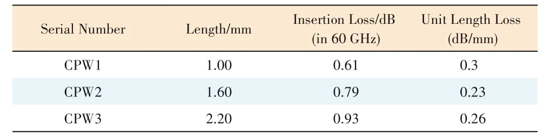
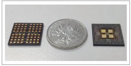
In this paper,a specific packaging prototype is made for a 5G communications equipment.It consists of 9 chips and a 64-unit antenna array,including 3 low power RF chips,2 through silicon via (TSV) transfer chips and 4 high-power chips.The TSV transfer chip is used to realize vertical signal transmission.Fig.13 is a schematic diagram of the structure of a 3D fan-out RF microsystem and antenna integrated proto⁃type.
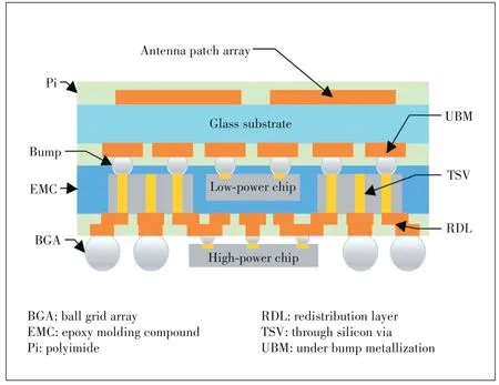
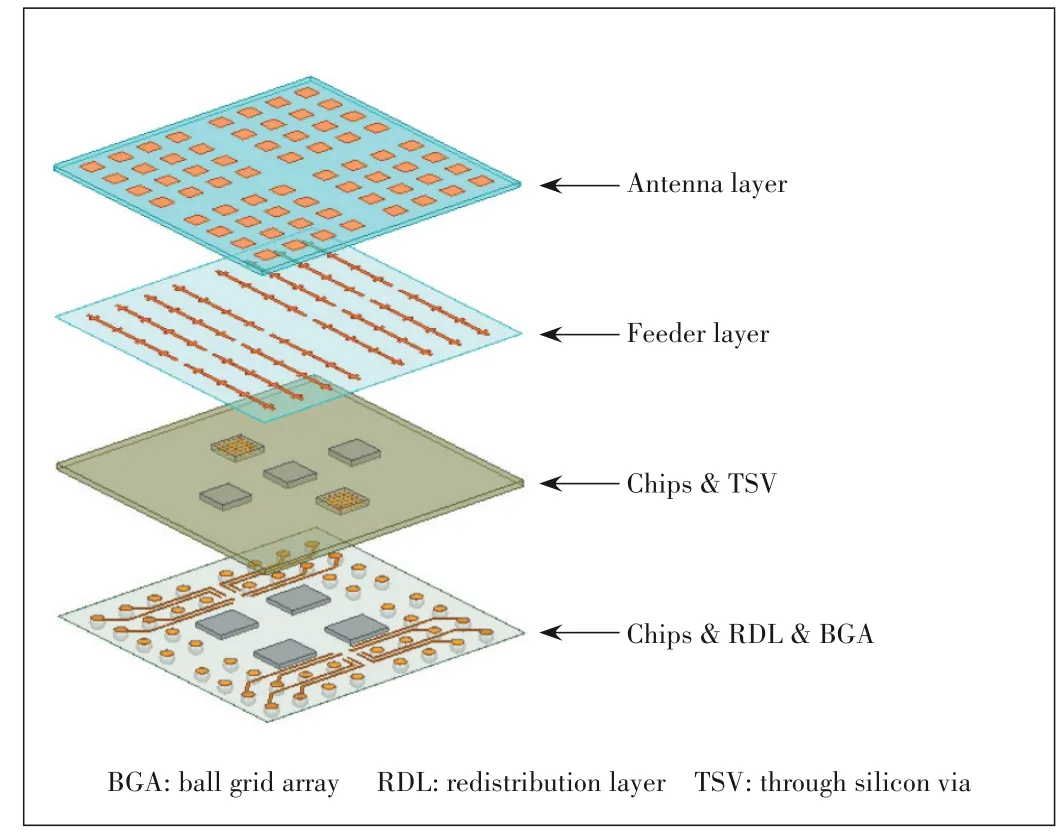
The architecture of AiP is depicted in Fig.14.The RF mod⁃ule demonstrates a multi-layer structure,with antenna and chip layers stacked vertically,and at the very top of the mod⁃ule,the antenna patch array as well as the feeding structure is fabricated on the glass substrate for Tx/Rx channels.As the kernel part,high power chips are embedded in the fan-out(FO) module and interconnected with RDL and TSV struc⁃tures to establish the transceiver sections;additionally the low⁃er power chips are attached beneath as the signal processing section,thus the solder balls can be arranged on the bottom side as in/out ports.The whole module can be soldered on the system board as an RF transceiver.
4.2 Fabrication Process of AiP
The integration of RF microsystem and antenna is realized by a new wafer-level 3D fan-out packaging process,different from the traditional 3D stacking packaging.In this paper,a permanent bonding process of resin wafer and glass wafer is adopted,and the BGA welding process is avoided between the two⁃layer wafers,which is very important for the requirement of low loss of RF devices.The interconnection system of RF devices and antennas is directly realized by RDL process.The wafer-level packaging technology takes the wafer as the pro⁃cessing object and carries out the packaging process directly on the wafer,which has high machining accuracy and consis⁃tency,and its wiring accuracy can reach 1 μm.The RF trans⁃mission loss of wafer-level packaging verified in the first sec⁃tion above shows that the transmission loss of RF interconnec⁃tion is very small,which will be very conducive to the integra⁃tion of RF microsystems and antennas.Fig.15 shows the packaging process of the 3D fan-out RF microsystem used in this paper.
▲Figure 12.Simulation results of antenna gain in working bandwidth.
▲Figure 13.Architecture of integrated prototype of 3D fan-out RF mi⁃crosystem and antenna.
▲Figure 14.3D fan-out RF microsystem.
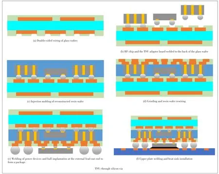
▲Figure 15.RF microsystem integration process.
The specific fabrication process of the RF micro-system and antenna integrated process prototype is as follows.First,a wiring layer and a passivation layer are formed successively on the front and the back of the glass wafer,and the passiv⁃ation layer is opened on the back of the glass wafer.The TSV transfer chip,the filter and the antenna tuner chip with bump are flip-welded to the opening of the passivation layer on the back of the glass wafer.Fig.16 shows a process photo of five chips flip-flopped to the back of the glass wafer.
And then the components such as the TSV transfer chip,the filter and the antenna tuner are coated with coating materi⁃al to form a reconstructed new wafer carrier,the back of which is thinned to expose the copper column welding disc surface of the TSV adapter plate,and a wiring layer,a passivation lay⁃er and a UBM layer are formed on its back.Then the power amplifier,low noise amplifier,transceiver control chip,power management chip and other components are soldered to the UBM layer on the back of the reconstructed new wafer.Solder ball bumps are grown at the UBM layer on the back of the re⁃constructed wafer carrier to form the final package.The pro⁃cess prototype of the integration of 3D fan-out RF microsystem and antenna is shown in Fig.17.
The integrated packaging process scheme of RF microsys⁃tem and antenna has the following advantages:
(1) The glass wafer and the resin wafer are bonded together,and there is no need to untie them in subsequent processing and use,which effectively solves the warping problem of the reconstructed wafer and improves the reliability of the prod⁃uct.At the same time,the integration of this process is also promoted.
(2) The processing technology of welding the chip assembly to the glass wafer and then wrapping it with coating material can effectively avoid the chip offset problem caused by the liq⁃uefaction flow of coating material and curing process in the tra⁃ditional coating forming process,and the processing precision is higher.Radio frequency signal transmission loss is lower.

▲Figure 16.Chips welded to the back of the glass wafer.
▲Figure 17.Process prototype of 3D fan-out RF microsystem.
(3) With the technology of wiring on the back of the glass wafer and then reconstructing the wafer with cladding,the double-sided wiring of the reconstructed wafer can be effec⁃tively realized,the complex temporary bonding process can be avoided,and the yield and reliability of the product can be im⁃proved,thus reducing the difficulty of product processing.
(4)In the final package,the low-power chip assembly is em⁃bedded in the coating material,and the high-power chip as⁃sembly is welded outside the coating material,which can ef⁃fectively solve the heat dissipation problem of the high-power chip,and when finally on the board,the back of the high-pow⁃er chip is coated with a thermal conductive material to con⁃nect the chip to the heat dissipation metal surface of the sub⁃strate to further improve the heat dissipation performance of the package.
5 Conclusions
In this paper,with 3D fan-out wafer-level rewiring technolo⁃gy,CPW planar transmission lines and stacked CPW transmis⁃sion structures are fabricated,and the RF transmission perfor⁃mance of CPW is verified.Through the test of CPW transmis⁃sion line by RF millimeter wave probe,the RF transmission loss of glass wafer in the range of 0–67 GHz is obtained.The results show that the RF transmission loss of the glass wafer is only 0.26 dB/mm in 60 GHz,and the loss introduced by the fan-out package is also very small,which indicates that the glass wafer can be used as the packaging substrate of RF de⁃vices.Then a slot coupling antenna for 5G communications is fabricated on a 12-inch glass wafer.The antenna works at 56.2 GHz and 63.8 GHz,and the maximum gain of the anten⁃na can reach 6 dB within the working bandwidth.On this ba⁃sis,an integrated prototype of 3D fan-out RF microsystem and antenna for 5G communications is designed and manufac⁃tured,and the prototype is fabricated through the wafer-level fan-out packaging process platform.The process of permanent bonding between the glass wafer and the resin wafer is adopt⁃ed,and the stacking process of the glass wafer and the resin wafer is avoided in the implementation process.In this way,the package has higher structural strength,higher reliability,less warping and lower process complexity,and shortens the processing cycle.Through the above conclusions,the effective⁃ness of glass wafer as RF device packaging is verified,and a feasible integrated solution of 3D fan-out micro-system and an⁃tenna is provided for 5G communications.

- ZTE Communications的其它文章
- Leaky-Wave Antennas for 5G/B5G Mobile Communication Systems:A Survey
- Multibeam Antenna Based on Butler Matrix for 3G/LTE/5G/B5G Base Station Applications
- A Novel 28 GHz Phased Array Antenna for 5G Mobile Communications
- Design of Millimeter-Wave Antenna-in-Package(AiP)for 5G NR
- Electromagnetic Simulation with 3D FEM for Design Automation in 5G Era
- Robust Digital Predistortion for LTE/5G Power Amplifiers Utilizing Negative Feedback Iteration