Design of Millimeter-Wave Antenna-in-Package(AiP)for 5G NR
(TMY Technology Inc.,New Taipei City,Taiwan 235,China)
Abstract: For 5G new radio (NR),there are two frequency bands:Frequency Range 1 (FR⁃1)(low frequency) and Frequency Range 2 (FR⁃2) (millimeter⁃wave frequency).Millimeter⁃wave has been officially utilized in mobile applications.The wide bandwidth is the key for the milli⁃meter-wave band.However,higher loss has become the major challenge for the wide use of this frequency range.Antenna array and beamforming technologies have been introduced to resolve the path loss and coverage problems.The key design considerations of the beamform⁃ing antenna array are low loss,compact system and small size.Antenna-in-package (AiP) has become the most attractive technology for millimeter-wave front-end system.For the design of AiP,many parameters such as RF transition,material and heat need to be considered and de⁃signed properly.The Over⁃the⁃Air (OTA) testing technology is also very critical for AiP mass production.In this paper,the detail of AiP design and new OTA testing technology are dis⁃cussed and demonstrated.
Keywords: 5G; antenna⁃in⁃package (AiP); beamforming; FR-2; millimeter⁃wave; new radio(NR);phased-array;low temperature cofired ceramic(LTCC)
1 Introduction
Antenna-in-package (AiP) is a technology that inte⁃grates antennas along with the transceiver and power dies into a system-in-package module.It has been widely used in the millimeter-wave antenna array such as 60 GHz gesture sensors,77 GHz automobile radars,94 GHz phased array,or even frequencies as high as 122 GHz for imaging sensors and 300 GHz for wireless links.5G milli⁃meter-wave spectrum can promise sufficient bandwidth to pro⁃vide the next⁃generation user experience and industrial appli⁃cations by using millimeter-wave as the carrier frequencies.
The idea of AiP technology can be traced back to the 90s when antenna designers had dedicated their time to minimiz⁃ing the size of the antenna.In the meantime,another idea was to integrate the antenna with the front-end system to achieve a more compact system.At an early development stage,AiP was developed together with Bluetooth technology.Later on,AiP was widely implemented into millimeter-wave radar systems.IBM,Intel,Samsung,Google,etc.,have realized the AiP mod⁃ules at 60 GHz,77 GHz,and 94 GHz.Recently,5G mobile communications and terahertz technology are becoming more and more important.Qualcomm has announced the world’s first 28 GHz AiP module for cellphone[1].Except for radar ap⁃plications,60 GHz is used for wireless communications of the IEEE 802.15.3c standard.Besides the AiP technology,anten⁃na-on-chip (AoC) has also been studied for 60 GHz,where the antenna is fabricated with other circuits on a wafer.AoC tech⁃nology is more suitable for terahertz applications.However,the efficiency of AoC is only 11.5%.Instead,AiP has shown high efficiency of more than 90% when low temperature co⁃fired ceramic(LTCC)[2]is used for manufacturing.
The requirements of AiP are multifunction,high-capacity and small size.The multilayer integration and package tech⁃nology have demonstrated its capability of low profile,low cost and potentially high-volume production.A proper multilayer design can help to improve the bandwidth and impedance match and lower the coupling effect between lines.For milli⁃meter-wave systems,the fabrication process and capability af⁃fect the performance significantly.High density interconnects printed circuit board (HDI PCB) and LTCC are conventional multilayer technologies.The microstrip line is the most com⁃mon technology for signal transmission between the layers.However,the flexibility of the microstrip line is limited by its two-dimensional structure.An innovative multilayer substrate integrated waveguide (SIW) is presented to give designers more freedom when designing AiP modules.SIW is an emerg⁃ing type of rectangular dielectric-filled waveguide which is fabricated by arrays of metallic vias to realize the bilateral edge or sidewalls.The three-dimensional structure supports very high flexibility when designing an AiP module[3].
In this paper,the design considerations and architectures will be discussed along with the capabilities and the prod⁃ucts of TMY Technology Inc.(TMYTEK).TMYTEK is a mil⁃limeter-wave company that specializes in 5G solutions such as AiP front-end modules,beamforming technologies and testing systems.
2 Design Considerations and Architectures
To fulfill the increasing demands in the millimeter-wave front-end module (FEM),AiP turns into the most promising and suitable technology to achieve the phased arrays cost-ef⁃fectively.At the same time,the material and process choices involving tradeoffs among engineering constraints are also con⁃sidered,including heat management,control design,RF per⁃formance,calibrations,and more(Fig.1).The solution to mul⁃tiple dimensional engineering problems is not linear and needs a lot of experience and creativity to realize the products.In addition to design,mass production is also a significant challenge,especially in Over-the-Air(OTA)testing.
2.1 System Architectures
Fig.2 shows three different architectures for the 5G phased array.In the antenna and beamformer architecture,the block shows an RF FEM with an analog beamformer which includes antenna array,duplexer and beamformer.Nowadays,a couple of beamformer chip makers have announced beamformer chips optimized for 5G millimeter-wave bands.The second ar⁃chitecture integrates intemediate frequency (IF)-radio frequen⁃cy (RF) conversion into the module as indicated in the rectan⁃gular block labeled with up and down conversion.Given that frequency converters dramatically affect the quality of commu⁃nication,embedding it into the system increases system perfor⁃mance and reduces the complication of integration.Integrat⁃ing mixers and filters in the package is not a trivial job,and lo⁃cal oscillator (LO)signal distribution is another concern,espe⁃cially in large,tiled array.The third architecture is based on open radio access network’s (ORAN’s) split option 7.2 to in⁃tegrate the low physical (Low PHY) layer into the module to offload the front-haul network on the radio access network(RAN).In this architecture,digital components are included,which raise the challenges to a new level.
2.2 Design Considerations
The design considerations of AiP are the multi-dimensional engineering problems due to its complexity and high density.This section is divided into four sub-sections:beamforming in⁃tegrated circuit (IC) and up/down converter chips,fabrication technologies and materials,design of antenna and transition,and design of feeding networks and filters.
2.2.1 Beamforming IC and Up/Down Converter Chips
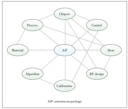
▲Figure 1.System context diagram of AiP design parameters.
A modern beamformer chip integrates power amplifiers(PAs),low noise amplifiers (LNAs),phase shifters (PSs),vari⁃able attenuators and T/R switches.Complementary metal ox⁃ide semiconductor (CMOS),CMOS silicon on insulator (SOI),and bipolar CMOS (BiCMOS) technologies are preferred due to the benefit of digital circuit integration and low cost,even if the output power is not as good as the III-V compound process⁃es such as GaAs and GaN.The main specifications that need to be considered are transmitter gain and power,receiver gain and noise,phase resolution and RMS error,attenuation range and resolution,memory size,beamforming control speed,pow⁃er consumption,and cost.In a 5G millimeter-wave phased ar⁃ray,the output power is not the only concern.Due to the fea⁃ture of Orthogonal Frequency Division Multiplexing (OFDM)in 5G,the power amplifier (PA) back-off operation is neces⁃sary.It is considered along with antenna array gain to form a system with targeted equivalent isotropically radiated power(EIRP) and reasonable power efficiency (Table 1).The design considerations of up/down converters are conversion gain,noise,linearity,LO pumping power,and isolations.
2.2.2 Fabrication Technologies and Materials
Fabrication technologies and materials are critical for the performance,cost,and size of the AiP module.There are three major technologies for AiP manufacturing:HDI PCB,LTCC and fan-out wafer-level packaging (FOWLP)[4].Table 2 shows the capability comparison of the three technologies.For the material selection,dielectric constant (Dk) and loss tangent(Df) are the main considerations.Thermal conductivity,Dk and Df change with temperature.Thickness ranges of core board and prepreg are also important in AiP design.Fig.3 shows the performances of Dk and Df with different materials.
2.2.3 Design of Antenna and Transition
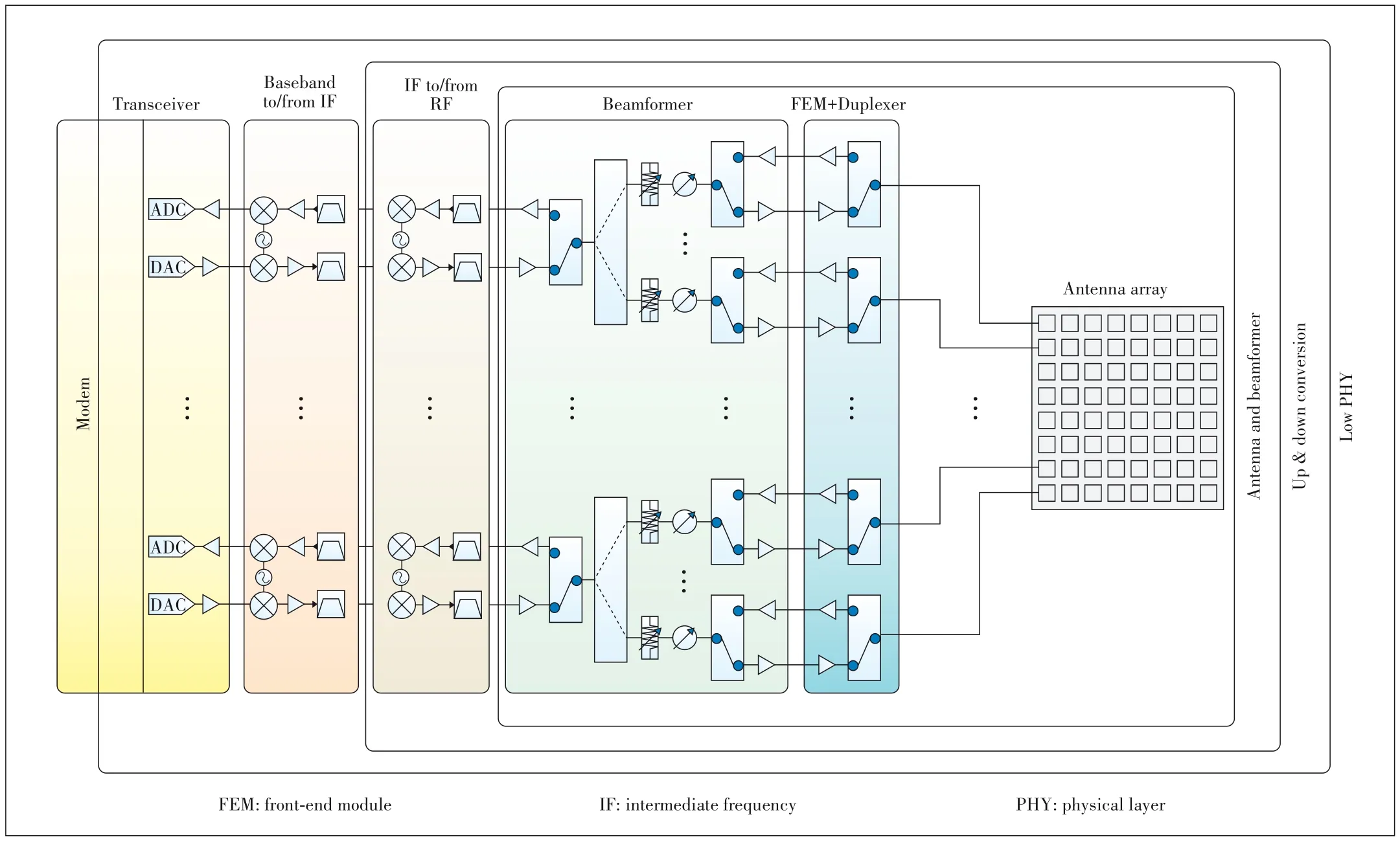
▲Figure 2.Three different system architectures of antenna⁃in⁃package(AiP)design.

▼Table 1.Beamforming design considerations and TMYTEK’s capability
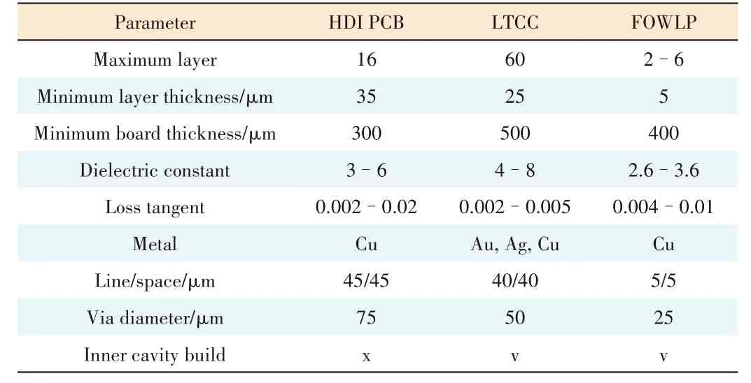
▼Table 2.Capability comparison of three main antenna⁃in⁃package(AiP)fabrication technologies

▲Figure 3.Dielectric constant and loss tangent of different materials.
In low frequency (FR-1),the antenna radiation pattern is typically designed as omnidirectional antenna.In millimeterwave frequency (FR-2),antenna array has become the essen⁃tial solution to compensating for the higher path loss at this frequency range.The consideration of the antenna array is dif⁃ferent compared with the design of single antenna,especially including the beamforming technology.Beam pattern,beam steering range,sidelobe suppression,beam pattern symmetry between two polarizations,antenna gain,isolation between ar⁃ray elements,antenna bandwidth,antenna efficiency,and re⁃turn loss are all the critical design parameters.Normally,the traditional planar antenna has a design of two layers,which is hard to have a good performance for the above parameters si⁃multaneously.The multilayer antenna technology has more de⁃sign flexibility to achieve better performance.However,the de⁃sign also becomes more complicated.The design of multilayer introduces the vertical structures such as the via wall into the antenna to improve the isolation or the director to improve the directivity.Nevertheless,the transition design between layers is the most critical part of this multilayer antenna design.A good transition design means having a better impedance match.The manufacturing process and capability affect the flexibility of transition and limit the final performance.Fig.4 shows the HDI type III stack and via types.It has two levels of microvias,buried vias and regular through-hole vias.The mi⁃crovias are used effectively in improving signal and power in⁃tegrity.

▲Figure 4.High density interconnects(HDI)type III structure[5].
2.2.4 Design of Feeding Networks and Filters
Building a feeding network is critical to the antenna array as the components cannot be placed off-board.Size and com⁃plexity are important for measuring feeding network perfor⁃mance.The commercial off-the-shelf (COTS) beamforming ICs has 4,8,or 16 channels.For 5G gNB,4 × 4 or 8 × 8 antenna array is used as a standard unit cell,which might operate as single or dual polarization.Since the feeding network connects the beamforming ICs and antenna elements,it has to incorpo⁃rate matching circuits to achieve wideband operation.Good isolation between dual-polarization ports has to be assured to achieve a low cross-polarization coefficient[6].The multilayer design which is described in the last section is also consid⁃ered for achieving a better impedance match of transition.
The filter design is limited to the board area available for passive components.The larger the room for filters,the better the rejection performance can be achieved.At the same time,thermal stability and repeatability are also challenging for de⁃signers to reduce the tuning effort to achieve an SMT-capable device.As an example of the microstrip structure,the toler⁃ance of substrate thickness,etching size and even dielectric constant should be considered and calculated carefully to achieve the best performance at the millimeter-wave range.
2.3 OTA Measurement for AiP Module
Conductive testing is no longer an option for the millimeterwave module implemented by AiP technology.There are no connectors or testing points available for the purpose.The on⁃ly way to characterize the module is through the OTA method.
Traditionally,a bulky chamber along with one or more me⁃chanical positioners needs to ensure the device under test’s(DUT’s) radiation pattern can be measured correctly and precisely,as shown in Fig.5[7].More recently,a com⁃pact antenna test range (CATR) technology has re⁃duced the size of the chamber but still retains the same concept of mechanical parts and testing items based on radiation patterns shown in Fig.6[8].The approach used for decades has become an indus⁃try standard for research and design.However,in the coming 5G era,the number of devices to be tested on the product line will overwhelm this old technology.A traditional chamber or CATR is a good tool for research and design purposes,but it is too slow and bulky for production lines.For ex⁃ample,the latest technology in the industry can get a pattern in about a few minutes,which is im⁃pressive if we compare it to our predecessors with a half-hour or longer testing cycles.However,achieving the level of seconds is still not guaran⁃teed.Furthermore,the nature of mechanical posi⁃tioners makes automation integration in product lines not a straightforward task.
A new method for OTA measurement of pro⁃duction lines is built for 5G millimeter-wave beamforming antenna arrays by TMYTEK[9].It adopts different approaches to meet the produc⁃tion demands of millimeter-wave AiP modules.The mechanical positioner is removed to speed up the OTA testing time.TMYTEK’s BBoxTMtechnology is used to measure the RF perfor⁃mance of a millimeter-wave module or device,in⁃cluding error vector magnitude (EVM),EIRP,fre⁃quency error,adjacent channel leakage ratio(ACLR),etc.[10–11].The system architecture is shown in Fig.7.The main idea is to measure AiP with another beamforming array(BBoxTM).This to⁃pology requires the calibration process to elimi⁃nate the phase and amplitude errors due to the angular misalignment between the two antenna patterns.The results are measured by a signal an⁃alyzer with a signal generator and integrate the up/down converters (UD Box) to down-convert the millimeter-wave signal to lower frequency.The measuring time is dramatically decreased since the scanning is done by electronic control.
3 Design Example
TMYTEK cooperated with NTK Technologies,Inc.[12],a Japanese LTCC technology company.A 4 × 4 LTCC unit AiP module for the 5G FR2 n261 band(27.5–28.35 GHz)has been designed by TMYTEK and manufactured by NTK.A larger 8×8 array is also demonstrated by tiling up to four-unit modules on one sin⁃gle motherboard.For the design of 5G NR millimeter wave beamforming antenna array,the size of the antenna array could be very different,i.e.4 × 4,8 × 8,16 × 16,even larger,for different applications.Therefore,the modularization meth⁃od provides a better way to configure a phased array system for adapting different dimensions of antenna arrays.

▲Figure 5.Traditional Over-the-Air(OTA)chamber system.

▲Figure 6.Compact antenna test range(CATR)chamber system.
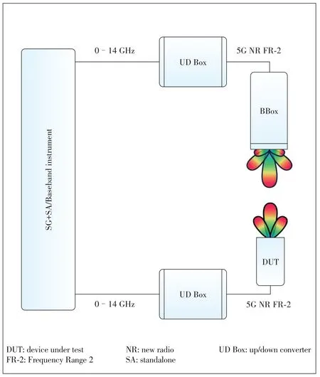
▲Figure 7.New over-the-air(OTA)system.
A 4 × 4 LTCC antenna-in-package front-end module (AiP FEM) is presented in this paper,along with the 28 GHz 8 × 8 phased array system which is fully integrated with four 4×4 AiP FEMs,an up/down converter and a phase-locked oscilla⁃tor.The AiP FEM is fabricated with a 26-layer LTCC process by NTK.It is integrated with four 4-channel beamformer chip⁃sets,power combiner,filter,mixer,frequency doubler and six⁃teen substrate integrated waveguide (SIW) antennas.Fig.8 shows three layers of the 26-layer LTCC AiP FEM.The input and output ports are the transmitting/receiving IF signals,LO source,digital control signals and DC power supply.The phase and amplitude of each antenna channel can be con⁃trolled independently for beam steering and beam shaping ca⁃pabilities.The serial peripheral interface (SPI) control inter⁃face is used for fast control of beamforming characteristics,and the highest SPI clock rate has reached 50 MHz.The di⁃mension of AiP FEM is 29.3 × 22.1 × 4.1 mm3(Fig.9).The cavity shown on the backside is designed for easy mounting of devices to form a different size of the phased array using these modularized AiP FEMs.
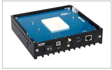
The 8 × 8 phased array system was integrated using four AiP FEMs mounted on the motherboard.For obtaining better phase noise,the local oscillator source was not embedded in the AiP FEMs; instead,they are integrated into the mother⁃board.Fig.10 shows the integrated system photo.There are two fans placed beside the AiP FEMs,which are not shown on the photo,to have better heat dissipation.

▲Figure 8.Three layers of the 26-layer low temperature cofired ceram⁃ic (LTCC) antenna-in-package front-end module:antenna,filter and combiner.

▲Figure 9.Top and bottom view of the 26-layer low temperature co⁃fired ceramic (LTCC) 4 × 4 antenna-in-package front-end module for 28 GHz band.
4 Conclusions
▲Figure 10.8 × 8 phased array system integrated with four antenna-inpackage front-end modules.
The design of millimeter-wave antenna-in-package is dis⁃cussed and an example from TMYTEK is presented in this pa⁃per.The millimeter-wave technology has become more and more important for communications and radar applications.Thus,the considerations for AiP mass production are very crit⁃ical for having better system performance and lower cost.This paper has discussed the manufacturing technologies and mate⁃rials.Moreover,the importance of the OTA measurement solu⁃tion is highlighted.TMYTEK has developed the best OTA so⁃lution for AiP mass production to accelerate the development of 5G millimeter-wave industries.
Acknowledgment
We would like to acknowledge the contributions and cooper⁃ation of the LTCC leading manufacture company,NGK,for the manufacturing of the 4×4 LTCC AiP substrate.
- ZTE Communications的其它文章
- Leaky-Wave Antennas for 5G/B5G Mobile Communication Systems:A Survey
- Multibeam Antenna Based on Butler Matrix for 3G/LTE/5G/B5G Base Station Applications
- A Novel 28 GHz Phased Array Antenna for 5G Mobile Communications
- Integrated 3D Fan-out Package of RF Microsystem and Antenna for 5G Communications
- Electromagnetic Simulation with 3D FEM for Design Automation in 5G Era
- Robust Digital Predistortion for LTE/5G Power Amplifiers Utilizing Negative Feedback Iteration

