Electronic structure of molecular beam epitaxy grown 1T-MoTe2 film and strain effect∗
Xue Zhou(周雪), Zeyu Jiang(姜泽禹), Kenan Zhang(张柯楠), Wei Yao(姚维),Mingzhe Yan(颜明哲), Hongyun Zhang(张红云), Wenhui Duan(段文晖), and Shuyun Zhou(周树云),2,†
1State Key Laboratory of Low Dimensional Quantum Physics and Department of Physics,Tsinghua University,Beijing 100084,China
2Collaborative Innovation Center of Quantum Matter,Beijing 100084,China
Keywords:quantum spin Hall effect,1T-MoTe2,molecular beam epitaxy(MBE),transition metal dichalcogenides(TMDCs)
1.Introduction
Topological materials have provided an important platform for exploring new physics and realizing novel quantum phenomena.[1,2]For example, quantum spin Hall effect(QSHE)[3–5]is expected in two-dimensional topological insulators.[6]Transition metal dichalcogenides(TMDCs)with distorted trigonal structurehave been predicted to be important candidates for realizing QSHE with potential applications in topological field effect transistors.[7–11]Recently,thin films have been revealed to show electronic properties compatible with QSHE.[12–14]-MoTe2has similar crystal structure to[15]and can also be a potential candidate for QSHE.MoTe2crystalizes in three structures,hexagonal(2H),monoclinic(),[15]and orthorhombic(Td).[16]Bulk single crystal ofMoTe2undergoes a phase transition to Tdphase[16]which hosts type-II Weyl fermions,[17–19]and a superconducting transition has been reported at even lower temperature,[20]however,mechanically exfoliated few layeredMoTe2has been reported to be a semiconductor.[15]
2.Methods
The density functional theory(DFT)calculations are performed using the Vienna ab initio simulation package(VASP)[32]with the Perdew–Burke–Ernzerhof(PBE)[33]exchange–correlation functional and a plane wave energy cutoff of 500 eV.A k-point grid of 16×20×1 is applied to sample the Brillouin zone. The pristine geometric structure of the monolayer is fully relaxed until the residual forces on each atom are less than 0.001 eV/˚A,and the obtained equilibrium lattice parameters are a=3.475 ˚A and b=6.367 ˚A.To simulate the uniaxial strain along the a-axis(b-axis),a stain is applied along the a-axis(b-axis),and the length of b-axis(aaxis)as well as the ionic positions is optimized until the residual forces are less than 0.001 eV/˚A.The spin–orbit coupling(SOC)effect has been taken into account in our calculations.
3.Results and discussion
Figures 1(a)and 1(b)show the top and side views of the crystal structure ofMoTe2. The Mo atoms deviate from the center of the octahedron formed by six Te atoms,forming zigzag Mo chains along the a-axis direction(see the top view in Fig.1(a))and distorted Te octahedra in the b–c plane(side view in Fig.1(b)). Graphene is a fantastic substrate for growing films with different crystal structures and symmetries through van der Waals epitaxiy,[34]and is used as the substrate for growingMoTe2film. Figures 1(c)and 1(d)show the RHEED and LEED patterns of the graphene/SiC substrate.Figures 1(e)and 1(f)show the RHEED and LEED patterns of theMoTe2films under optimum growth conditions. Sharp streaky stripes(indicated by yellow arrow in Fig.1(e))and six diffraction spots(Fig.1(f))from theMoTe2film are observed in the RHEED and LEED patterns,respectively. TheMoTe2film grows mainly along the same orientation as the graphene substrate with a small distribution of azimuthal angles in the LEED pattern due to the weak van der Waals growth with weak coupling between theMoTe2film and graphene.Because of the different crystal symmetries between the substrate(three-fold symmetry)and theMoTe2film(two-fold symmetry),there are three equivalent orientations ofMoTe2films on graphene,leading to apparently hexagonal LEED patterns,similar to the case ofWTe2film[12]and the previous report onMoTe2[29]yet with better LEED pattern.The observation of diffraction spots from both theMoTe2film and the graphene substrate suggests that theMoTe2film is atomically thin,∼1 monolayer(ML)thick.Increasing the growth time leads to weaker diffraction spots from the substrate and the graphene diffraction spots disappear at 2 ML(see Appendix A),however,no major change in the electronic structure is observed since the difference in the electronic structure of monolayer,bilayer,and multilayerMoTe2films is small due to the small band splitting. Using the lattice constants of graphene as a reference,the extracted in-plane lattice constants ofMoTe2from the LEED pattern are a=3.47and b=6.48,suggesting a 2%(tensile)strain along the b-axis direction compared to the lattice constants of a=3.48and b=6.33in the bulk crystal.[15]

Fig.1.Crystal structure of MoTe2 and diffraction patterns from RHEED and LEED.(a)and(b)Top and side views of the crystal structure of MoTe2.Red and green balls represent Te and Mo atoms,respectively.The dashed box indicates the unit cell.RHEED patterns of(c)the graphene/SiC substrates and(e)the as-grown MoTe2 sample.LEED patterns of(d)the graphene/SiC substrates and(f)the as-grown MoTe2 sample measured at a beam energy of 120 eV.The white and yellow arrows indicate the patterns from graphene and MoTe2,respectively.
The growth condition is critically dependent on the substrate temperature.Figure 2 shows a systematic study of the RHEED and LEED patterns of the films grown at different substrate temperatures while maintaining other experimental conditions fixed.When the substrate temperature is 331◦C,no detectable signals from MoTe2are observed in the RHEED(Fig.2(a))or LEED patterns(Fig.2(e)).Only in a small temperature window of ∼25◦C between 338◦C and 363◦C,streaky stripes can be observed(indicated by the yellow arrows)in RHEED(Figs.2(b)–2(d))and diffraction spots are observed in the LEED patterns(Figs.2(f)–2(h)).The sharpest streaky stripes from the RHEED pattern(Fig.2(c))and the best signal from the LEED pattern(Fig.2(g))obtained at the substrate temperature of 350◦C indicate that the optimum growth condition includes the substrate temperature of 350◦C.

Fig.2.RHEED and LEED patterns for films grown at different substrate temperatures.(a)–(d)RHEED patterns after growing at the substrate temperature of 331 ◦C,338 ◦C,350 ◦C,and 363 ◦C,respectively.(e)–(h)Corresponding LEED patterns.The yellow and white arrows indicate diffraction spots from MoTe2 and graphene,respectively.

Fig.3.Electronic structure of MoTe2 revealed by ARPES measured at ∼10 K.(a)Intensity maps measured from EF to −0.84 eV with an integrated energy window of 50 meV.(b)ARPES spectrum measured along the Γ–X direction(marked by dotted line in(a)).(c)Zoom-in dispersion near EF.(d)Calculated dispersions along the Γ–X direction(blue)and (red)and(e)zoom-in dispersion near EF with a uniaxial strain of 2%along the b-axis direction and a shift −0.09 eV in energy.
Figure 3 shows the electronic structure ofMoTe2revealed by in situ ARPES measurements.Figure 3(a)shows the intensity maps measured from EFto −0.84 eV.Since the 2HMoTe2is a semiconductor with a gap of larger than 1 eV,[37]this confirms that the measured band dispersion is not from the 2H-MoTe2but from theMoTe2.A hexagonal pocket centered at the Γ point is observed at EFand its size increases at low energies,suggesting that it is a hole pocket. Below−0.56 eV,a new pocket emerges at the Γ point and further splits into two circular pockets,resulting in three hole pockets in total at −0.84 eV.Figure 3(b)shows the dispersions measured along the Γ–X direction.The dispersion shows a linear dispersing hole pocket through EFand two parabolic bands below −0.56 eV,consistent with the intensity maps in Fig.3(a).Figure 3(c)shows a zoom-in of the dispersion near EF. In addition to the hole pocket near EFas discussed above,there is another dispersing band within −0.15 eV,suggesting that this is likely the electron pocket from the conduction band.Figures 3(d)and 3(e)show the calculated band dispersion for comparison.[12]By using the extracted experimental lattice constant from LEED,which indicates a strain of 2%(tensile)along the b-axis direction,a good agreement with the experimental results is obtained.The overall band structure is similar to that ofWTe2,[12,38]yet with two major differences.Firstly,the two bands below −0.56 eV almost cross(pointed by the red arrow in Fig.3(b)),which is different from those in theWTe2film and is not discussed in previous work onMoTe2.[12]Indeed,the better agreement between the ARPES data and the calculated band structure of the strained film compared to the calculated result of the unstrained film in previous work[12]also indicates the important role of stain in this material.Secondly,both the experimental and calculated results reveal an overlap between the conduction and valence bands,while dopedWTe2has been reported to be an insulator with a gap of 45 meV.[12]Therefore,our ARPES data and calculation show that different fromWTe2,the as-grownMoTe2film is metallic with an overlap between the valence and conduction bands.
Since the electronic structures ofMoTe2films[7]and bulk crystals[39–41]are strongly dependent on the strain,we calculate the evolution of the electronic structure with uniaxial strain to provide more insights.Figure 4 shows the calculated band structure of monolayerMoTe2film under uniaxial strain along the b-axis(Figs.4(a)–4(e))and a-axis(Figs.4(f)–4(j))with strains ranging from −2%to 3%.The application of a tensile strain along the a-axis direction has similar effect to the application of a compressive strain along the b-axis direction.The uniaxial strain has two major effects.Firstly,it changes the splitting of the two bands below −0.5 eV at the Γ point.More importantly,it changes the energy position of these valence bands significantly,while maintaining the energy position of the conduction band.By applying a tensile strain along the a-axis,the overlap between the valence and conduction bands decreases,until eventually a gap of 47 meV emerges at 3%strain(Fig.4(j)).The opening of such a band gap is critical,since it makesMoTe2potentially a quantum spin Hall insulator if the Fermi energy is further tuned to inside the gap region.Therefore in order to realize QSHE inMoTe2films,a tensile strain(3%)along the a-axis is needed.
4.Conclusion
To summarize,we have successfully grown high-quality atomically thinMoTe2films using MBE after a systematic investigation of the growth at different substrate temperatures,which is confirmed by RHEED,LEED,and ARPES measurements.Furthermore,ARPES measurements show that the as-grown film is a metal with an overlap between the conduction and valence bands,which is attributed to the strain effect.Comparison of calculated band structures at different strains further suggests that a suitable tensile strain(3%tensile strain along the a-axis direction)can induce a significant gap between the conduction and valence bands.Our work not only reports the MBE growth conditions for obtaining 1T-MoTe2thin film and its experimental electronic structure,but also provides insights for band structure engineering ofMoTe2film to make it a quantum spin Hall insulator.
Appendix A:Supplemental material
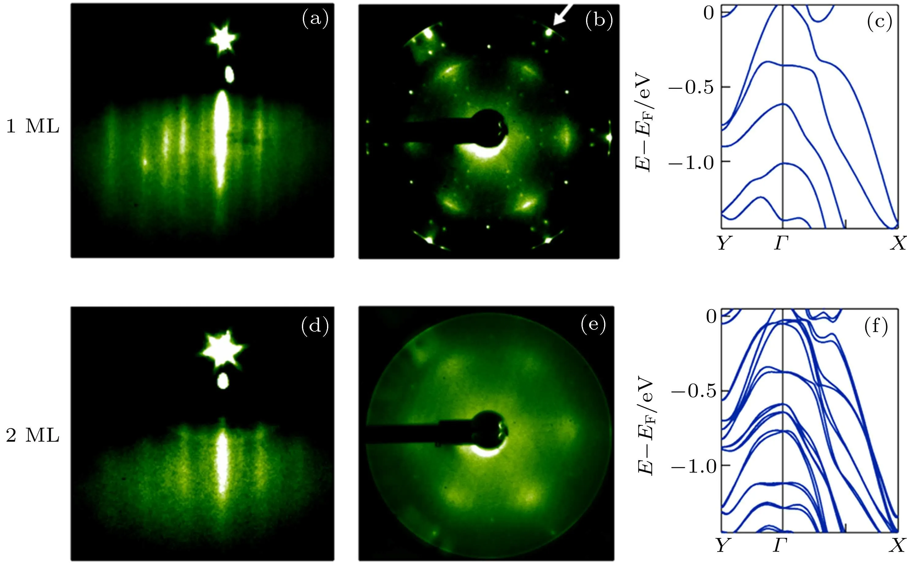
Figure A1 shows a comparison of RHEED,LEED,and calculated electronic structure for 1 ML and 2 ML films.The observation of graphene spots in Fig.A1(b)shows that the sample is ∼1 ML.By doubling the growth time,the diffraction spots from graphene disappear.A comparison of the electronic structures for 1 ML and 2 ML shows that the splitting is very weak and beyond the resolution of the ARPES experiments.

Fig.A1.Comparison of RHEED,LEED,and calculated electronic structure for 1 ML and 2 ML films.(a)–(c)RHEED,LEED,and calculated electronic structure of 1 ML film,white arrow in(b)indicates the patterns from graphene.(d)–(f)RHEED,LEED,and calculated electronic structure of 2 ML film.
- Chinese Physics B的其它文章
- Compact finite difference schemes for the backward fractional Feynman–Kac equation with fractional substantial derivative*
- Exact solutions of a(2+1)-dimensional extended shallow water wave equation∗
- Lump-type solutions of a generalized Kadomtsev–Petviashvili equation in(3+1)-dimensions∗
- Time evolution of angular momentum coherent state derived by virtue of entangled state representation and a new binomial theorem∗
- Boundary states for entanglement robustness under dephasing and bit flip channels*
- Manipulating transition of a two-component Bose–Einstein condensate with a weak δ-shaped laser∗

