单层,少层和块状WS2薄膜中声子位移随温度的变化
2019-10-14 07:56刘新科王佳乐许楚瑜罗江流梁迪斯岑俞诺吕有明李治文
物理化学学报 2019年10期
刘新科,王佳乐,许楚瑜,罗江流,梁迪斯,岑俞诺,吕有明,李治文
深圳大学材料科学与工程学院,深圳市特种功能材料重点实验室,深圳大学南山区生物聚合物与安全评价重点实验室,广东 深圳 518060
1 Introduction
Two-dimensional transition metal dichalcogenides (TMDs)have recently gained much interest due to their rich physical and chemical properties, which enable the future applications in nano-electronics1,2, nano-photonics3-5, and valley-electronics6-8.The counterpart graphene, has also been intensively investigated due to its high electron mobility ~200000 cm2·V-1·s-1, since its first mechanical exfoliation by Novoselov et al. in 20049,10.However, due to its absence of bandgap, to achieve high current on/off ratio is difficult for graphene-based devices. Several techniques have been proposed to create the bandgap for graphene.For example, employing quantum mechanical confinement in patterned11or exfoliated graphene nano-ribbons12introduces a bandgap up to 400 meV, and applying perpendicular electric field (voltage exceeding 100 V) in bi-layer graphene creates a bandgap up to 250 meV13. These innovative methods of introducing a bandgap in graphene always come with a price of significant mobility degradation (~200 cm2·V-1·s-1), process complexity, or device reliability under high voltage14-16. For TMDs, such as MoS2, MoSe2, WSe2, and WS2etc, these materials have a bandgap, which is tunable based on the number of layer. Usually, the bandgap of the bulk TMDs is ~1.2-1.3 eV,and one of mono-layer TMDs is ~1.8-2.1 eV, the increase of bandgap with decreasing number of layer for TMDs is due to the carrier quantum confinement at an atomic scale. Being able to achieve atomic thickness and have a bandgap larger than that of silicon, TMDs are also attractive for being used as the channel material for Si CMOS devices beyond sub-22 nm, since TMDs have advantage for suppressing the source-to-drain tunneling current in ultra-short transistors and offering superior immunity to short-channel effects17.
Among TMD group, MoS2in both mono- and few-layer films has been intensively studied in the research community over the years18-23. MoS2-based field effect transistors (FETs) with excellent electrical characteristics have been demonstrated, such as high current on/off ratio (~108), low subthreshold swing (~70-80 mV·dec-1), mobility up to ~200 cm2·V-1·s-1(in highk/MoS2/high-k structure)24. As a typical TMD, WS2 has been widely used due to its potential excellent performance25. Similar to MoS2, WS2can also be grown through chemical vapor deposition (CVD)26. According to the simulation work by Liu et al.27, WS2 have a lower in-plane electronic mass, compared with MoS2, MoSe2, and MoTe2, which shows the potential for higher carrier mobility or higher output current for WS2-based FETs.However, as compared with MoS2, the experimental studies on WS2 are limited, or more work is required to be done for further harnessing the full potential of WS2-based FETs. In the literature, mono- and multi-layer WS2-based FETs were demonstrated, and achieved on/off current ratio of ~106-108with mobility of ~140-234 cm2·V-1·s-128-30.
As for the nano-electronic application, it is important to investigate the electron-phonon interaction and vibration properties of WS2. Raman spectroscopy, as an effective and nondestructive approach for phonon vibration study, has been used to evaluate graphene, and TMDs31-33. Raman spectra reveal much useful information of the test sample through Raman peak position and Raman shape change. Temperature dependent phonon shifts of single layer WS2by mechanical exfoliation34and multi-layer WS2by hydrothermal method35, have been investigated by Raman spectroscopy. In this work, we present thickness- and temperature-dependent studies of the phonon vibration mode for mono-layer, few-layer, and bulk WS2films prepared by mechanical exfoliation.
2 Experimental
The mono-layer (1L), few-layer (FL), and bulk WS2films were prepared on 300 nm SiO2/Si wafer by mechanical exfoliation from bulk WS2crystal, which was purchased from 2D Semiconductor Inc. 3M scotch-tape was used for transferring the WS2films. Raman and photoluminescence (PL) spectra were collected in a Renishaw inVia confocal system in the backscattering configuration. The wavelength of the laser was 514 nm (2.4 eV) from an argon ion laser, the grating of 2400 grooves·mm-1was used to obtain more details of line shapes of the Raman band. The laser power on the sample was set at around 1.0 μW to avoid laser induced heating. The application of a 100× objective lens with a numerical aperture of 0.9 can provide us a spot size of ~1 μm, and spectral resolution was 1 cm-1. The Si peak at 520 cm-1was used as a reference for wavelength calibration. Atomic force microscopy (AFM)images were obtained under tapping mode using Bruker Dimension Icon.
3 Rseults and Discussion
The atomic force microscopy (AFM) images of 1L, FL, and bulk WS2films are shown in Fig. 1a, b, and c. The film thickness was directly measured by AFM in a non-contact mode. As shown in Fig. 1d, e, and f, the step height or thickness of 1L, FL, and bulk WS2films were measured to be 0.98, 10, and 76 nm. Based on the reported mono-layer WS2thickness of ~0.9 nm, the number of layer for 0.98, 10, and 76 nm is determined to be 1L,~11 L, and ~84 L, respectively. In Fig. 2, PL spectra were measured using a 514 nm excitation laser. It is known that the bulk WS2is an indirect bandgap semiconductor with a ~1.3 eV bandgap, whereas 1L WS2has a direct bandgap of ~2.1 eV. For the bulk WS2, the electron states involved in the indirect transition (the valence band maximum at Γ point and the conduction band minimum at T point) originate from linear combination of tungsten d-orbital and sulfur pz-orbital, and their dispersion strongly depends on the number of layers. For the 1L WS2, the electron states involved in the direct transition (the valence band maximum at K point and the conduction band minimum at K point) mainly originate tungsten d-orbital, and their energies are not very sensitive to the number of layers36. In Fig. 2, one sharp PL peak centered at ~638.5 nm is observed for 1L WS2and the measured spectral range nearly vanishes for the FL WS2sample. When the thickness decreases to 1L, the dramatic increase of the PL intensity is a signature of the transformation from indirect to direct bandgap structures. Based on the PL peak for 1L WS2shown in Fig. 2, the bandgap of 1L WS2is estimated from the PL peak to be ~1.94 eV, which is smaller than ~2.1 eV. Direct electronic transitions in 1L WS2originate from exitonic radiative relaxation, and for this reason the PL peak signal always appears at energies slightly lower than~2.1 eV direct bandgap of WS2.
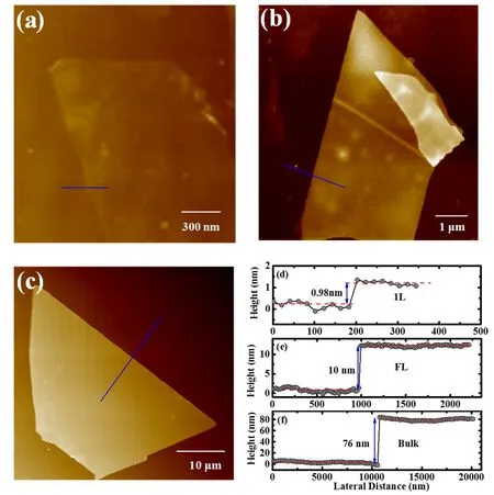
Fig. 1 The atomic force microscopy (AFM) images of (a) 1L, (b) FL, and (c) bulk WS2 films.The step height or thickness of (d) 1L, (e) FL, and (f) bulk WS2 films.
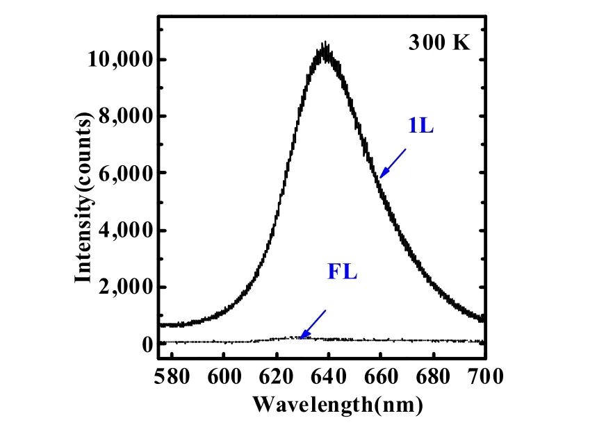
Fig. 2 Photoluminescence spectra from FL to 1L. One sharp PL peak centered at ~638.5 nm for 1L WS2, however nearly no peak for the FL sample.
Raman studies of 1L, FL, and bulk WS2films have been carried out using a 514 nm excitation laser, since Raman spectrum of WS2under a 514 nm excitation laser becomes very rich, revealing many second-order peaks37,38. Raman spectra at 300 K of 1L, FL, and bulk WS2films are shown in Fig. 3a, b,and c. Raman active modes of WS2comprise of A1g, E1g, E12g, and E22gat the center of the Brillouin zone, but E1gis forbidden in the back-scattering configuration and E22g is less studied due to its low frequency out of the most conventional Raman spectral range. The A1gmode is related to the out-of-plane vibration of sulfur atoms, and the E12gmode is associated with the in-plane vibration of tungsten and sulfur atoms. Under a 514 nm excitation laser, the A1g(Γ) mode was observed at 419 cm-1and dominant 2LA(M) mode observed at ~350 cm-1overlapping with E12g(Γ) mode (~355 cm-1), which was acquired by multi-Lorentzian fitting. Fig. 3d, e, and f show the multi-Lorentzian fitting of 2LA(M)-2 E22g(Γ), E12g(M), 2LA(M), and E12g(Γ) modes for 1L, FL, and bulk WS2films, respectively. When the number of layer increases from 1L to bulk, the A1g(Γ) mode shows a blueshift of 1.34 cm-1from 419.14 to 420.48 cm-1, similar to the trend observed for MoS2, as the van der Waals interactions between the layers increase the restoring force in the thicker layers. On the other hand, E12g(Γ) mode shows a red-shift of 0.69 cm-1from 354.59 (1L) to 353.90 cm-1(bulk), which is attributed to the increment of dielectric long-range coulomb interactions among the effective charges. It is worth noting that in WS2, the close proximity of the 2LA(M), and E12g(Γ) modes increases the error in determining the frequency shift. As compared with MoS2, the A1g(Γ) blue-shift of 1.34 cm-1and the E12g(Γ) red-shift of 0.69 cm-1of WS2are much smaller, as the A1gblue-shift and the E12gred-shift of MoS2as increasing 1L to bulk is ~4.2 and 2.2 cm-1, respectively. As shown in Fig. 3, the frequency difference(Δ) between A1g(Γ) and E12g(Γ) modes is varied from 64.55 to 66.58 cm-1, when the number of WS2layer increases from 1L to bulk. The Δ between A1g(Γ) and E12g(Γ) modes for 1L WS2prepared by mechanical exfoliation is reported to be 64 cm-1by Thripuranthaka et al.34. In the literature, Δ between A1g(Γ) and E12g(Γ) modes is also increased from ~62 to 65 cm-1, when the number of WS2 layer increases from 1L to bulk prepared by chemical vapor deposition (CVD) method. Although this observed trend is similar to that of MoS2, there are a larger Δ change between A1g(Γ) and E12g(Γ) modes (from ~19 to ~25 cm-1), when the number of MoS2layer increases from 1L to bulk. It is noted that the Δ (~18 cm-1) between A1g and E12g modes for the 1L MoS2 by mechanical exfoliation is smaller than that of 1L MoS2by CVD method (~19 cm-1). However, based on the reported values in the literature, the case for WS2is opposite,since the Δ (~64 cm-1) between A1g(Γ) and E12g(Γ) modes for the 1L WS2by mechanical exfoliation is larger than that (~62 cm-1)of 1L WS2 by CVD method. Further, it looks that Raman vibration mode for WS2 is less sensitive to the number of layer as compared to MoS2. Δ between A1gand E12gmodes is often used to identify the number of layer in MoS2films. Due to the less sensitivity of Δ between A1g(Γ) and E12g(Γ) modes to the number of layer for WS2, more accurate or robust method is needed for identifying the number of layer in WS2 films, except for the AFM direct measurement method.
Temperature-dependent Raman measurements of 1L, FL, and bulk WS2films have been carried out at 80-300 K under a 514 nm excitation laser, and the results are show in Fig. 4a, b, and c.In this part, we will focus on the discussion about peak intensity ratio [2LA(M)/A1g(Γ), E12g(Γ)/A1g(Γ), etc.] and peak position as a function of temperature. In viewing of WS2 as the potential CMOS channel material beyond Si, it is important to study the electron-phone interactions or vibration modes under various temperatures through non-destructive Raman method. The temperature-dependent Raman vibration modes of WS2can have a direct bearing on the carrier transport of WS2-based FETs. As shown in Fig. 5, the 2LA(M)/A1g(Γ), E12g(Γ)/A1g(Γ), and Rec.[2LA(M), E12g(Γ)]/A1g(Γ) peak intensity ratio are plotted as a function of temperature for (a) 1L, (b) FL, and (c) bulk WS2.Rec. [2LA(M), E12g(Γ)] is the recombination of 2LA(M) and E12g(Γ) modes, or the mode without multi-Lorentzian fitting. The peak intensity of Rec.[2LA(M),, and A1g(Γ) as a function of temperature for 1L, FL, and bulk WS2 films can be referred to Fig. 5. With the temperature decreasing,the Raman intensities of Rec. [2LA(M), E12g(Γ)], 2LA(M), E12g(Γ),and A1g(Γ) are increasing at different rates for 1L, FL, and bulk WS2 films. As shown in Fig. 5, it is noted that the Rec. [2LA(M),E12g(Γ)]/A1g(Γ) intensity ratio is creased to more than 1 at 230,190, and 160 K, respectively, for 1L, FL, and bulk WS2films.The A1g(Γ) vibration mode, related to the out-of-plane vibration of sulfur atoms, is dominated when the temperature is above the“cross-over” point or intensity ratio more than 1; Rec.[2LA(M),E12g(Γ)] mode, related to film disorder and in-plane vibration of tungsten and sulfur atoms, is dominated when the temperature is below “cross-over” point or intensity ratio less than 1. The“cross-over” phenomenon is mainly caused by the fast increasing intensity of 2LA(M) mode as the temperature decreasing. Based on the “cross-over” temperature, it may be possible to determine the layer number of WS2 films, since it shows layer-dependent behavior, although more detailed work is needed.
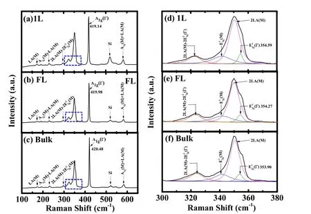
Fig. 3 Raman spectra at 300 K of (a) 1L, (b) FL, and (c) bulk WS2 film under a 514 nm excitation laser. Multi-Lorentzian fitting of 2LA(M) - modes for (d) 1L,(e) FL, and (f) bulk WS2 film, respectively.
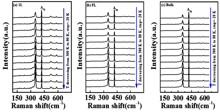
Fig. 4 Temperature-dependent Raman measurements of (a) 1L, (b) FL, and (c) bulk WS2 films at 80-300 K under a 514 nm excitation laser.
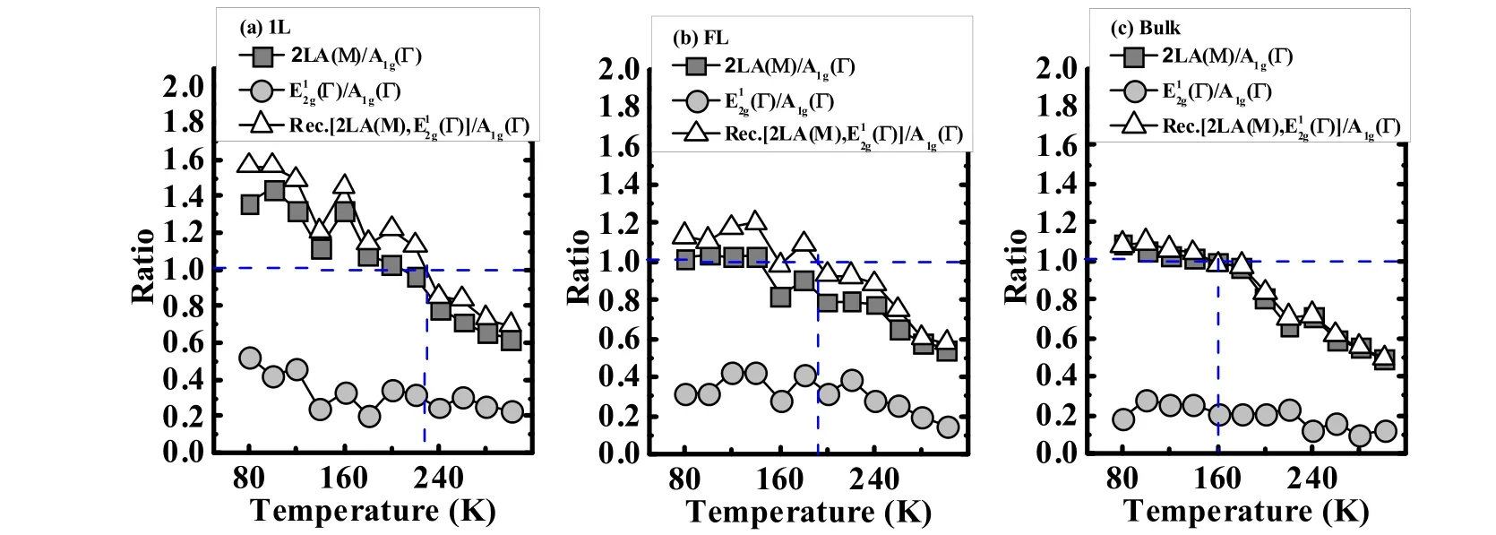
Fig. 5 2LA(M)/A1g(Γ), E12g(Γ)/A1g(Γ), and Rec. [2LA(M), E12g(Γ)]/A1g(Γ) peak intensity ratios as a function of temperature for (a) 1L,(b) FL, and (c) bulk WS2 films.It is noted that the Rec.[2LA(M), E1 2g(Γ)]/A1g(Γ) ratio is creased to more than 1 at 230, 190, and 160 K, respectively, for 1L, FL, and bulk WS2 films.
When the temperature decreasing from 300 to 80 K, all the Raman modes of 2LA(M), E12g(Γ), A1g(Γ), and A1g(M) + LA(M)for 1L, FL, and bulk WS2 films change linearly as a function of temperature, shown in Fig. 6a, b, c, and d. It is well-known that Raman spectroscopy is a photon-phonon process which is dominant over thermal expansion, as well as the phonon process on the Raman mode linearly shifts with change in temperature.A few data point dispersion for the Raman peak position can be expected and is well-understood due to the slight variation in the laser spot on the sample, or the local Raman stage vibration, or low excitation power on the sample followed by the extra attenuation from the cold-hot cell window during the measurement. The observed data of peak position obtained from Lorentzian fitting for 2LA(M), E12g(Γ), A1g(Γ), and A1g(M) +LA(M) modes versus temperature were fitted using the Grüneisen model: ω(T) = ω0 + XT, where ω0 is the Raman mode peak position at zero Kelvin temperature, and X is the first-order temperature coefficient of the same mode. The slope of fitted lines gives the first-order temperature coefficient of the specific Raman mode, and shown as an inset in Fig. 6. X values of 2LA(M), E12g(Γ), and A1g(Γ) modes for the 1L WS2are larger than those of FL and bulk WS2, shown in Fig. 6a, b, and c. However,X (~-0.010 cm-1·K-1) of A1g(M) + LA(M) mode is almost identical for 1L, FL, and bulk WS2. Table 1 summarizes the extracted first-order temperature coefficient of LA(M), 2LA(M)- 2E22g(Γ), E12g(M), 2LA(M), E12g(Γ), A1g(Γ), and A1g(M) + LA(M),for 1L, FL, and bulk WS2. The X values for the 2LA(M), A1g(Γ),and A1g(M) + LA(M) modes of 1L WS2 in this work were observed to be close or nearly same as the reported one by Thripuranthaka et al.34. The X variation of E12g(Γ) between this work and Ref.34could be due to the error caused by multi-Lorentzian fitting. Also, the reported X for E12g(Γ) and A1g(Γ)modes of 1L WS2grown by CVD method is -0.0125 and-0.0149 cm-1·K-1, respectively, which is larger or one order magnitude higher than the ones reported in this work and Ref.34.In addition, the reported X for and E12gand A1gmodes of 1L MoS2by mechanical exfoliation method, is ~-0.017 and ~-0.013 cm-1·K-1, respectively, which is larger or one order magnitude higher than the ones reported in this work and Ref.39-41. This indicates that the thermal stability of WS2 may be better than that of MoS2, based on the first-order temperature coefficient of the Raman modes. As compared to X (~-0.0162 cm-1·K-1) of G peak for 1L graphene by mechanical exfoliation, X of 1L WS2in this work is also about one order magnitude lower. With the combination of lower in-plan electronic mass and higher thermal stability (or lower temperature coefficient)42, WS2 could serve as a better candidate for Si CMOS channel material beyond sub-22 nm, as compared to other TMDs. By now, temperaturedependent Raman studies have not been carried out for FL and bulk WS2films by mechanical exfoliation in the literature. The presence of substrate 300 nm SiO2/Si in this work may not affect the final results of temperature coefficient a lot. The effect of substrate on temperature coefficient of WS2 grown by CVD has been investigated by Peimyoo et al.39, and only gives about 6%variation. It is interesting to note that we did not observe the dependence of FWHM on the temperature in the examined temperature range in the 1L, FL, and bulk WS2samples. This is in contrast with the A1g FWHM temperature dependent for MoS2. Further, the variation in the Raman peak position as a function of temperature for the 1L, FL, and bulk WS2samples is due to the temperature contribution that consequences from anharmonicity and contribution from the thermal expansion or volume contribution.
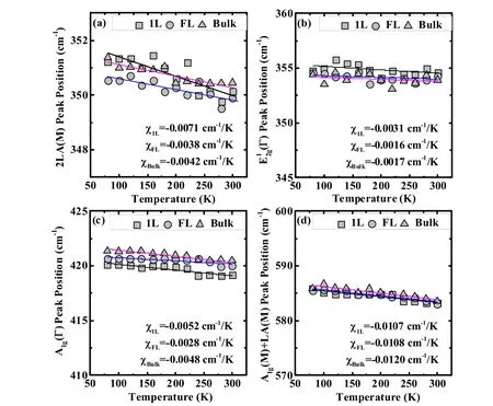
Fig. 6 Effect of temperature variation on the Raman modes of (a) 2LA(M), (b) E12g(Γ), (c) A1g(Γ), and (d) A1g(M) + LA(M) for 1L, FL, and bulk WS2 films.
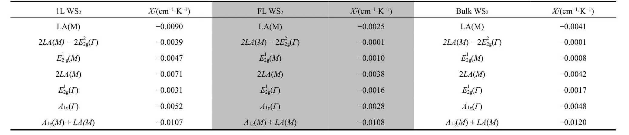
Table 1 Extracted temperature coefficient X for 1L, FL, and bulk WS2 films.
4 Conclusions
We have systematically investigated the thickness- and temperature-dependent Raman studies of the phonon vibration mode for mono-layer (1L), few-layer (FL), and bulk WS2films prepared by mechanical exfoliation. With the film thickness increasing to bulk, A1g(Γ) and E12g(Γ) modes show blue-shift of 1.34 cm-1and red-shift of 0.69 cm-1, respectively, with respect to 1L WS2. With temperature decreasing, all the Raman peak positions shift to a higher energy. The “cross-over” temperature,when the dominant Raman vibration modes swaps between E12g(Γ) and A1g(Γ), was identified to be 230, 190, and 160 K,respectively, for 1L, FL, and bulk WS2films. As compared to MoS2, WS2shows much smaller frequency change (64.55-66.58 cm-1) between E12g(Γ) and A1g(Γ) as the film thickness varying,and one magnitude lower temperature coefficient of Raman peak position or better thermal stability. Through this systematic study, the results shown here provide a physical guidance for WS2-based device engineering.
猜你喜欢
表面工程与再制造(2022年1期)2022-05-25
汽车实用技术(2022年5期)2022-04-02
今日农业(2021年7期)2021-07-28
舰船科学技术(2021年12期)2021-03-29
深圳大学学报(理工版)(2020年6期)2020-11-14
电子竞技(2019年22期)2019-03-07
电子竞技(2019年21期)2019-02-24
电子竞技(2019年20期)2019-02-24
电子竞技(2019年19期)2019-01-16
国外科技新书评介(2016年12期)2017-04-17