
Improved Hole Injection Property of Solution-Processed MoO3 with UV-Ozone Treatment
2018-11-16 02:58:50DONGDanMINZhiyuanLIUJunHEGufeng
物理化学学报 2018年11期
DONG Dan, MIN Zhiyuan, LIU Jun, HE Gufeng
National Engineering Lab for TFT-LCD Materials and Technologies, Shanghai Jiao Tong University, Shanghai 200240, P. R. China.
Abstract: The hole injection layer (HIL) plays a significant role in determining the performances of organic light-emitting diodes(OLEDs), especially when hole transport materials with deep highest occupied molecular orbital levels (HOMOs) are employed.Intensive efforts have been devoted to exploring novel hole injection materials with good solution-processing abilities in recent years. In this study, the solution-processed molybdenum trioxide(s-MoO3) is prepared via an ultra-facile method. Three different s-MoO3 layers prepared by three different methods, viz. layers annealed at 150 °C (s-MoO3 (150)), layers annealed at 150 °C and then processed in UV-ozone for 15 min (s-MoO3 (150, UVO)), and layers processed in UV-ozone for 15 min without annealing (s-MoO3 (UVO)), are obtained to investigate their influences on hole injection. The device with the s-MoO3 (150)layer has the lowest current density and the largest driving voltage, showing poor hole injection ability. In contrast, with the s-MoO3 (150, UVO) layer as HIL, the OLED produces a greatly enhanced current and sharply reduced driving voltage,comparable to the device using vacuum-evaporated MoO3. Similar results are obtained for the device with the s-MoO3(UVO) film, suggesting that high-temperature annealing is not essential for the s-MoO3 film with UV-ozone treatment. Hole injection efficiencies of MoO3 films are quantitatively characterized by analyzing the space-charge-limited current of holeonly devices; the hole injection efficiencies of s-MoO3 (150, UVO) and s-MoO3 (UVO)-based devices are ~0.1, far exceeding that of the s-MoO3 (150)-based device (10-5). XPS analysis is performed to detect the impact of the above treatments on the surface electronic properties of the s-MoO3 films. A typical characteristic of Mo5+ species is obtained for the s-MoO3 (150) film and a high-binding-energy shoulder appears in the O 1s peak of the s-MoO3 (150) film, indicating the existence of oxygen vacancies and oxygen adsorbed at the surface of s-MoO3 (150) film. When UV-ozone treatment is applied to this s-MoO3 (150) film, it produces a decrease of Mo5+ state and elimination of oxygen-rich adsorbates,resulting in MoO3 stoichiometry similar to that of the vacuum-evaporated MoO3 film. Consequently, a maximum current efficiency of 48.3 cd·A-1 is realized with the optimized UV-ozone treated s-MoO3 HIL. It This UV-ozone treated s-MoO3 should have widespread applications in low-cost solution-processed OLEDs as an excellent hole injection layer.
Key Words: Hole injection property; Solution process; Organic light-emitting diode; Stoichiometry; UV-ozone treatment
1 Introduction
Organic light-emitting diode (OLEDs) have attracted significant attention in display and lighting fields, due to their potentials for homogenous large-area emission, light weight and flexibility1–4. With the development of emitting materials and the optimization of the device structures, the current efficiency of OLEDs can reach nearly 200 cd·A-15. Enormous efforts have been devoted to improve the device performances by introducing novel OLED structures and tuning the charge carrier balance. Xu et al.6demonstrated a highly efficient and wide color-range tunable fluorescent OLED using two complementary undoped ultrathin emitters with an interlayer between them. A novel exciplex-forming host is employed in highly simplified device7.Besides, an efficient OLED is realized with substitutionally Boron-doped graphene anode8. However, many of these high efficiency devices are fabricated by thermal evaporation, which need high costs and have limit on large area panels. In contrast,solution processing, such as spin-coating, screen printing and inkjet printing can effectively avoid these drawbacks9–11. In order to facilitate hole injection and reduce the operating voltage, an effective strategy is to obtain a good energetic match at the electrode-organic interface by inserting an interfacial layer12,13. Poly(3,4-ethylenedioxyth-iophene):poly(styrenesulfonate) (PEDOT:PSS) is widely used as a hole injection layer(HIL) in solution-processed OLEDs because of its easily solution-processable ability, the smooth character of the resulting interlayer and suitable work function (4.8–5.2 eV)14.However, there still exists a large hole injection barrier from PEDOT:PSS when some hole transport materials (HTMs) with deep highest occupied molecular orbital (HOMO) levels are employed, such as 4,4’-bis(9-carbazolyl)-biphenyl (CBP) (-6.1 eV)15, resulting in high driving voltage and low current efficiency (CE). Moreover, the acidity and hygroscopicity of PEDOT:PSS will cause the problem of device stability16,17.
As an alternative to PEDOT:PSS, transition metal oxides(TMOs) have been a research focus due to their high work function and marked hole injection property, such as molybdenum oxide (MoO3)18–25, vanadium oxide (V2O5)26–29,and nickel oxide (NiO)30,31. In general, thermally-evaporated MoO3is an n-type semiconductor with very deep lying electronic states, whose work function is about 6.9 eV18.However, air-exposure will contaminate the surface of the metal oxide film and reduce its work function. Irfan et al.25demonstrated a sharp reduction on the work function of MoO3 from 6.8 to 5.6 eV after being exposed in air for one hour.Hancox et al.29found that the atmosphere of spin-coating and annealing could seriously affect the work function and stoichiometry of V2O5. Our group19introduced an ultra-facile synthetic route for solution-processed MoO3anode buffer layer and its work function is only 5.35 eV with air exposure, which is not high enough to improve the hole injection to the HTM with deep HOMO levels. Hence, the work functions of solutionprocessed TMOs are mostly decreased compared to those of their vacuum-evaporated counterparts. Recently, the surface treatment has been proposed to recover the work functions of TMOs, such as annealing in vacuum or nitrogen25,31,32, and oxygen plasma treatment24. Unfortunately, those processes usually require high temperature (200–400 °C) and complicate the fabrication, which is not conductive to reduce cost.
In this paper, we investigated the influences of different treatments on solution-processed MoO3(s-MoO3) HIL. It is found that the UV-ozone treated s-MoO3 film exhibits a decrease of Mo5+state and elimination of oxygen-rich adsorbates,resulting in a similar MoO3stoichiometry and hole injection efficiency to the vacuum evaporated MoO3film. The green phosphorescent OLED (PHOLED) with UV-ozone treated s-MoO3HIL shows a maximum current efficiency of 48.3 cd∙A-1,which is comparable to the device with evaporated MoO3(e-MoO3) (50.6 cd·A-1).
2 Experimental
The MoO3solution was prepared by dissolving 175 mg MoO3powder (Sigma-Aldrich) into 1 mL ammonia-water (Shanghai Lingfeng Chem. Reagent Co., Ltd., AR) in an ultrasonic bath(HangZhou BoKe Ultrasonic Equipment Co., Ltd.) for one minute. And then it was diluted by deionized water to a concentration of 10 mg·mL-119.
The chemicals were purchased from commercial sources and used as received. Hole transporting materials of 4,4’-bis[N-(1-naphthyl)-N-phenylamino] (NPB) and CBP and the electron transporting material of 1,3,5-tri(phenyl-2-benzimidazole)benzene (TPBi) were purchased from Taiwan Nichem Fine Technology Co., Ltd. The phosphorescent emitter of tris(2-phenyl-pyridine)iridium (III) (Ir(ppy)3), the electron injection material of lithium fluoride (LiF) were purchased from Beijing Aglaia Technology Co., Ltd. The Al cathode was purchased from ZhongNuoXinCai Co., Ltd.
OLEDs were fabricated on ITO-coated glass substrates(KINTEC Company) which were cleaned successively using deionized water, acetone (CMOS) and isopropanol (CMOS)under an ultrasonic bath for 15 min each time, then dried with nitrogen. To eliminate the adsorbate and solvent on ITO, the substrates were heated at 150 °C for 15 min, followed by being exposed to UV ozone (Sunmonde Electric Light Source Technology (Shanghai) Co., Ltd.) for 10 min. The basic configuration of the green phosphorescent OLED is ITO/HIL/NPB or CBP (40 nm)/CBP:(Ir(ppy)3) (8%, 20 nm)/TPBi (60 nm)/LiF (1 nm)/Al (100 nm). The s-MoO3layer was spin coated from the previously prepared solution at 9000 r·min-1for 60 s and the films were annealed at 150 °C for 10 min in air. Then,the annealed films were treated with UV ozone for different time.Subsequently, the samples were transferred into a high vacuum deposition system, and the organic layers were thermally deposited at a base pressure of 6.7 × 10⁻⁴Pa. The deposition rate was measured with quartz crystal. The evaporated MoO3was deposited at a rate of 0.01–0.05 nm·s-1and the total thickness is 3 nm, whereas the organic materials, except for the dopants,were evaporated at a rate of 0.1–0.15 nm·s-1. At the end, 100-nm-thick aluminum was deposited as the cathode. The proposed energy level of materials used is shown in Fig. 1.
The current density–voltage–luminance (J–V–L)characteristics of devices were measured using a computer controlled Keithley 2400 and Topcon BM-7A measurement system under ambient atmosphere. The XPS measurement was carried out in a Kratos AXIS Ultra DLD ultrahigh vacuum surface analysis system with a monochromatic aluminum Kαsource (1486.6 eV) under a base pressure of 1.33 × 10⁻⁷Pa. The samples of MoO3film were deposited on ITO-coated glass substrates.
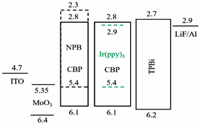
Fig. 1 The proposed energy levels of the materials used in devices.
3 Results and discussion
Firstly, to explore the hole injection property of our prepared s-MoO3, green phosphorescent OLEDs employing the s-MoO3with HTMs (NPB and CBP) which have different HOMO levels are fabricated, and the e-MoO3/HTL one is also fabricated for comparison. The current density-voltage characteristics of the devices are shown in Fig. 2a. Obviously, the device with s-MoO3/NPB has a low onset voltage of 2.2 V, indicating that the hole could inject into NPB from s-MoO3effectively19. When NPB is replaced by CBP with a deeper HOMO level (-6.1 eV)as HTM, the device exhibits a much lower current density and higher onset voltage (5.0 V), showing a poor hole injection property. This is consistent with the larger energy barrier between s-MoO3and CBP. However, the e-MoO3HIL can inject holes to CBP quite well, and significantly larger current and lower onset voltage of 2.6 V is obtained. This significant difference may be attributed to the higher work function of e-MoO3 (6.9 eV) as reported by Kröger18. Accordingly, the maximum current efficiencies of the s-MoO3/NPB, s-MoO3/CBP, and e-MoO3/CBP-based devices are about 35.5, 0.4,and 43.0 cd·A-1, respectively. The above results demonstrate that our s-MoO3does possess an effective hole injection property.Besides, the s-MoO3has poorer hole injection ability to HTMs with deeper HOMO levels than the evaporated MoO3. As a result, to improve the hole injection and the performances of such OLEDs, it is essential to increase the work function of s-MoO3.
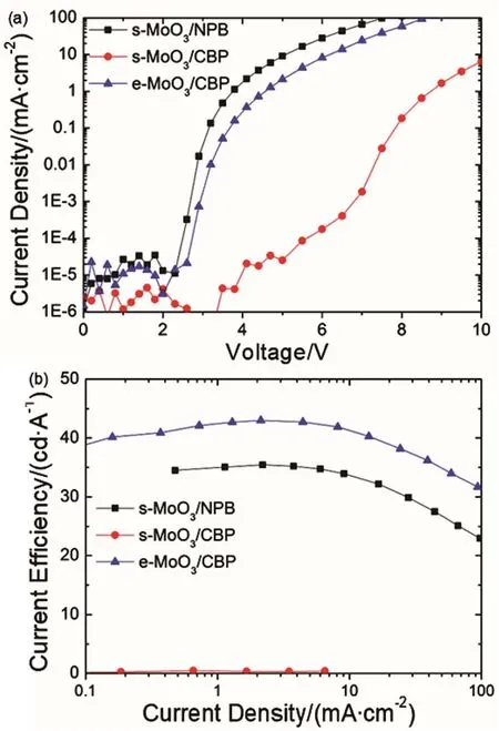
Fig. 2 (a) Current density–voltage and (b) current efficiency characteristics of the OLEDs with s-MoO3/NPB, s-MoO3/CBP,e-MoO3/CBP.
Various treatment processes including annealing in air and exposure in UV-ozone are applied on s-MoO3film to investigate their influences on hole injection. To be concise, the three different methods are abbreviated as following: layers annealed at 150 °C, s-MoO3(150); layers annealed at 150 °C and then processed in UV-ozone for 15 min, s-MoO3(150, UVO); layers processed in UV-ozone for 15 min without annealing, s-MoO3(UVO). Correspondingly, these differently treated s-MoO3films combined with CBP HTM are employed in the green PHOLED.For comparison, a control device with e-MoO3 HIL is fabricated as well.
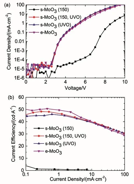
Fig. 3 (a) Current density–voltage and (b) current efficiency–current density characteristics of the OLEDs with s-MoO3 (150), s-MoO3(150, UVO), s-MoO3 (UVO) and e-MoO3 HTL.

Table 1 Summarized performances of the solution-processed OLEDs incorporating e-MoO3 HIL and s-MoO3 HILs with different treatments.
Fig. 3 shows the J–V and CE–J characteristics of these devices with differently treated MoO3films, and Table 1 summarizes the detailed results. The reference device with e-MoO3reveals a high current density, along with a low onset voltage of 2.6 V as mentioned above. In contrast, the device with s-MoO3 directly annealed at 150 °C under ambient shows a much higher onset voltage (5.0 V), suggesting that this treated s-MoO3 film has a relatively low work function and hence a large hole injection barrier exists. However, with UV-ozone treatment for 15 min on the s-MoO3(150) HIL, the current density of device is significantly enhanced and the onset voltage sharply decreases to 2.6 V, showing a great improvement on the hole injection ability. The maximum current efficiency of the device with s-MoO3(150, UVO) markedly increases from 0.7 to 48.3 cd∙A-1,which approaches that of e-MoO3-based device (50.6 cd∙A-1).More surprisingly, if the s-MoO3film is just directly treated with UV-ozone for 15 min without the 150 °C annealing process, the OLED with s-MoO3 (UVO) HIL has a comparable performance(Vonset = 2.6 V, CEmax = 46.1 cd∙A-1) to the device with s-MoO3(150, UVO). This suggests that high temperature annealing process is inessential for the s-MoO3film with UV-ozone treatment. The UV-ozone treatment is of great importance for the s-MoO3film as HIL in solution-processed OLEDs.
To unravel the origin of the significant enhancement on the performances of s-MoO3based devices with UV-ozone treatment, the impact of different treatments on the surface electronic properties of the s-MoO3films was analyzed using XPS measurement. Fig. 4a shows the full scan spectrum of the e-MoO3 and s-MoO3 (150, UVO) films. O 1s and Mo 3d peaks are characteristics of MoO3. Additional sharp peaks of In 3d, Sn 3d, attributed to the ITO, are also detected, indicating that the MoO3 films are very thin (less than 5 nm). In Fig. 4b, the four MoO3films with different treatments have the identical Mo 3d5/2peak at 233.05 eV, and Mo 3d3/2peak at 236.15 eV,corresponding to the Mo6+state, suggesting these MoO3 films are almost stoichiometric MoO3composition33. Differently, a secondary Mo 3d doublet (Mo 3d5/2at 231.2 eV and Mo 3d3/2at 234.3 eV) exists in s-MoO3 (150) film, which is the typical characteristic of Mo5+species. This indicates that oxygen vacancies exist in the s-MoO3(150) film, resulting in the gap states caused by the partial filling of unoccupied Mo 4d levels34,35.In addition, Fig. 4c depicts that a high binding energy shoulder appears in O 1s peak of the s-MoO3(150) film, and a fit of this shoulder yields a peak of 532.9 eV, which is attributed to oxygen adsorbed at the surface of s-MoO3film21. When UV-ozone treatment is applied on this s-MoO3(150) film, the shoulder disappears, suggesting that oxygen-rich adsorbates are effectively removed.
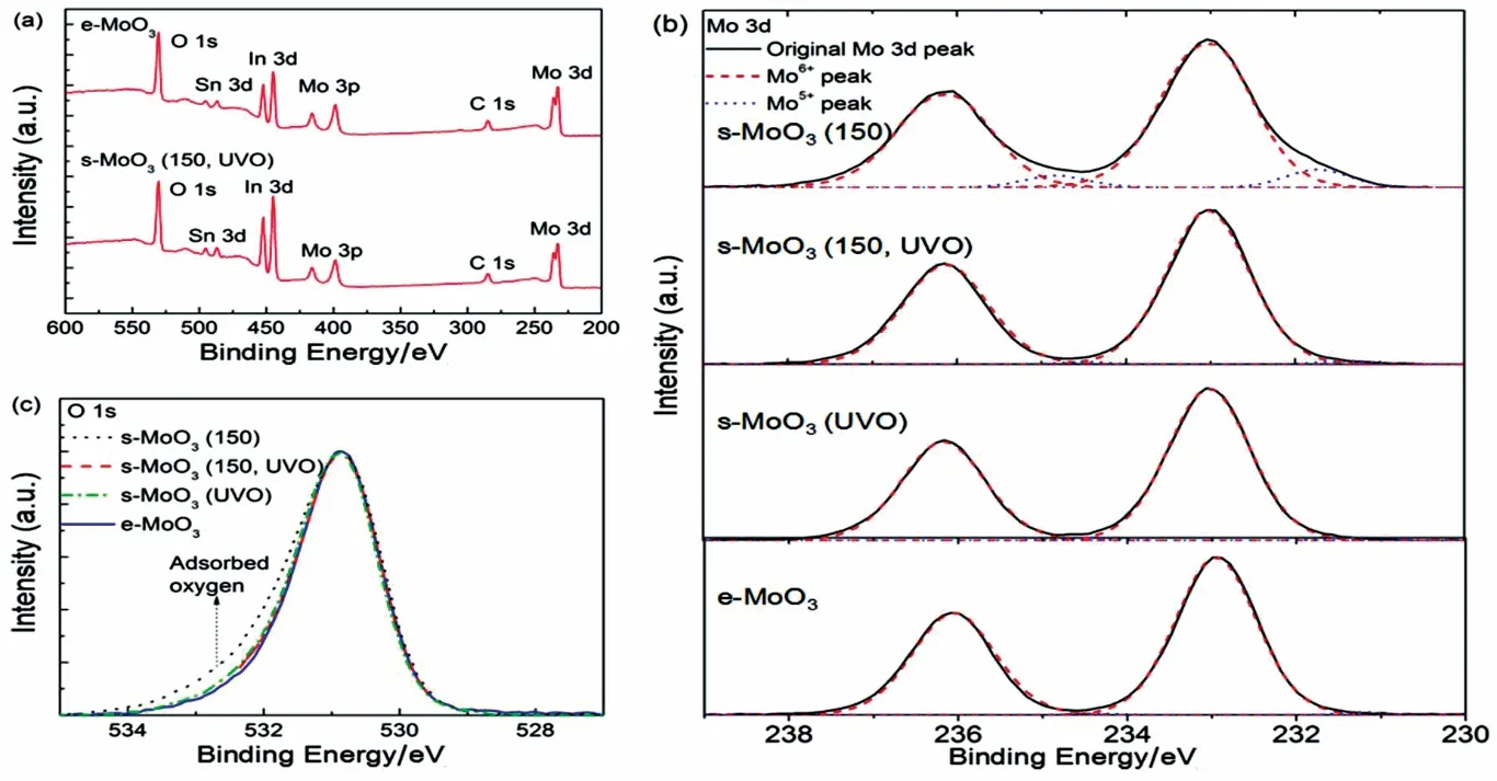
Fig. 4 XPS spectra of e-MoO3 and s-MoO3 films with different treatments.(a) Full scan, (b) O 1s core level, (c) Mo 3d core level.
These results indicate that UV-ozone treatment can effectively tune the surface electronic properties of the s-MoO3films,increasing the Mo5+films to Mo6+and decreasing the oxygenrich adsorbates in the s-MoO3(150), making the almost same stoichiometric s-MoO3composition with the e-MoO3film. As a result, a considerable enhancement is obtained in device performance with the UV-ozone treatment.
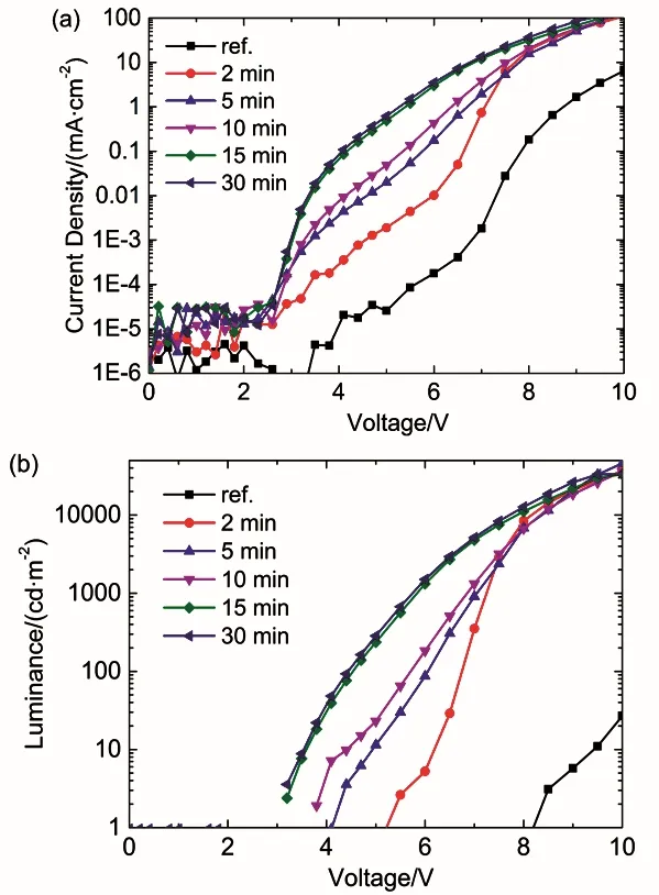
Fig. 5 (a) Current density–voltage, (b) luminance–voltage characteristics of the devices with different UV-ozone treatment time of s-MoO3 and the s-MoO3 (150) as reference.
To investigate the effect of UV-ozone treatment to s-MoO3 thin film in detail, the performances of devices with different UV-ozone treatment time are compared in Fig. 5. The device with s-MoO3(150) HIL is also chosen as a reference. It is clearly seen that the hole injection is remarkedly improved when the s-MoO3is treated by UV-ozone and the onset voltage decreases from 5.0 V to below 3 V. Besides, the current density increases as increasing the treatment time up to 15 min. However, a longer UV-ozone treatment time (30 min) hardly shows any further improvement, meaning that the improvement on work function and hole injection property are saturated when the treatment time increases to 15 min. The luminance characteristic shows a similar trend. The luminance of UV-ozone treated devices are increased to 33000–46000 cd·m-2at 10 V due to the enhancement on the hole injection and more balanced charge carriers, far exceeding that of the s-MoO3(150) one (27 cd·m-2).
The hole injection property of MoO3 films can be quantitatively characterized by analyzing the space charge limited current of hole-only devices. Fig. 6a shows the J–V characteristic of hole-only devices with configuration of ITO/HIL/CBP (345 nm)/e-MoO3 (10 nm)/Al (100 nm). The s-MoO3 films are treated with different methods as mentioned above and the e-MoO3 is also included for comparison. The theoretical space-charge-limited current density (JSCLC) is calculated from equation (1)36.
where µ0 is the zero-field mobility of CBP (set to be 10-3cm2·(V·s)-1)37, ɛ0is the permittivity in free-space (8.85 × 10⁻¹⁴C·(V·cm)-1), ɛr is the dielectric constant (assumed to be 3.0), E is the applied electric field and d is the cavity length. The Poole-Frenkel slope β is the field-dependent mobility coefficient. β can be obtained from independent time-of-flight experiments, and is found to be 1.3 × 10⁻³(cm·V)-1/213.
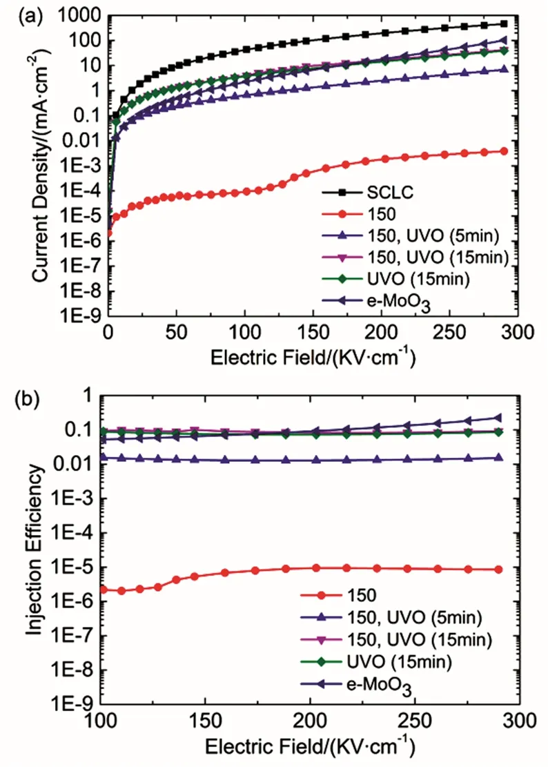
Fig. 6 (a) Current density–electric field and (b) hole injection efficiency–electric field characteristics of the hole-only devices with e-MoO3 and s-MoO3 films of different UV-ozone treatment time.
The current density is enhanced with the time of UV-ozone treatment increased from 0 min to 15 min and close to that of e-MoO3device. Moreover, the device with s-MoO3(UVO) has a comparable hole injection property to the device with s-MoO3(150, UVO). These results coincide with the performances of devices presented in Fig. 3 and Fig. 5. Additionally, the current densities of all devices are much lower compared to the theoretical JSCLC, suggesting that the hole injection contacts in those devices are not ohmic. Hence, the hole injection efficiency(ƞINJ) can be obtained from equation (2).

where JINJis the measured steady-state current density. The e-MoO3shows a hole injection efficiency of ~0.1, consistent with the results previous reported13,19. The injection efficiencies of s-MoO3(150, UVO) and s-MoO3(UVO)-based devices are about 0.1, as shown in Fig. 6b, while the maximum injection efficiency of s-MoO3(150)-based device is at the order of 10-5. It demonstrates that the optimized s-MoO3films with UV-ozone treatment have superior hole injection property, comparable to the e-MoO3.
4 Conclusions
In summary, by introducing different treatments on solutionprocessed MoO3films, the influences on modifying the hole injection ability to HTMs with deep HOMO levels in OLEDs are investigated. The UV-ozone treatment can effectively tune Mo5+to more highly oxidized Mo6+state and remove some oxygenrich adsorbates in the solution-processed MoO3films even without annealing process. Besides, such effects are more pronounced at longer treatment time up to 15 min. As a result,the reduced work function of solution-processed MoO3films can be enhanced and hence improve the hole injection property,making it comparable to the evaporated MoO3film. The work provides a simple and effective way to realize efficient hole injection for solution-processed MoO3in OLEDs whose HTM has a deep HOMO level by UV-ozone treatment.

- 物理化学学报的其它文章
- K+ Concentration-Dependent Conformational Change of Pb2+-Stabilized G-quadruplex
- Wide Bandgap Random Terpolymers for High Efficiency Halogen-Free Solvent Processed Polymer Solar Cells
- Asymmetric Quinoxaline-Based Polymer for High Efficiency Non-Fullerene Solar Cells
- L-3,4-dihydroxyphenylalanine and Dimethyl Sulfoxide Codoped PEDOT:PSS as a Hole Transfer Layer: towards High-Performance Planar p-i-n Perovskite Solar Cells
- Growing Carbon Quantum Dots for Optoelectronic Devices
- Fluorination: An Effective Molecular Design Strategy for Efficient Photovoltaic Materials