金属氧化物与现代微电子学
——过渡金属前体化合物及转化为材料的化学过程
Tabitha M.Cook Adam C.Lamb 薛子陵
金属氧化物与现代微电子学
——过渡金属前体化合物及转化为材料的化学过程
Tabitha M.Cook Adam C.Lamb 薛子陵*
(田纳西大学化学系,诺克斯维尔市,田纳西州 37996,美国)
金属氧化物薄膜如HfO2(被称为高k电介质)是现代微电子器件的关键组件,广泛用于计算机(平板电脑,笔记本电脑和台式机)、智能电话、智能电视、汽车和医疗设备中。具有大介电常数(k)的金属氧化物已经取代了介电常数小的SiO2(k=3.9),从而使得微电子元件进一步小型化。过渡金属化合物在化学气相沉积(CVD)和原子层沉积(ALD)中被广泛用作前体,通过与O2、H2O或O3的反应生成金属氧化物薄膜。微电子金属氧化物膜是纳米材料最广泛应用的一个领域。本文概观该领域的最新进展,包括我们对d0过渡金属配合物与O2反应的研究。
金属氧化物;栅极电介质材料;薄膜;微电子学;化学气相沉积;原子层沉积
0 Introduction
Microelectronic devices are a major part of society today.There has been a continuous drive to make computers,tablets,smartphones and other such devices smaller,faster and more efficient.Over the past few decades,there has been steady progress in this area following Moore′s law,which states that thenumber of transistors to fit onto integrated circuits doubles approximately every two years[1-2].By increasing the number of transistors on the circuits,microelectronic deviceshave become more competent,smaller with a longer battery life.To this end,new designs for the components of microelectronic devices as well as the materials used to make them need to be developed.
Among many designs of the field-effect transistor(FET),one is the complementary metal oxide semiconductor (CMOS)utilizing both p-and n-type metaloxide silicon field-transistors (MOSFET)[3-4].Until recently,MOSFETs in these devices had a planar,2D design (Fig.1).These transistors typically have four main parts:source,gate,drain and substrate.An insulating layer,or gate oxide layer,separates the metal gate from the source and drain.This layer is made of dielectric materials,which is polarized when placed in an electric field[3-5].
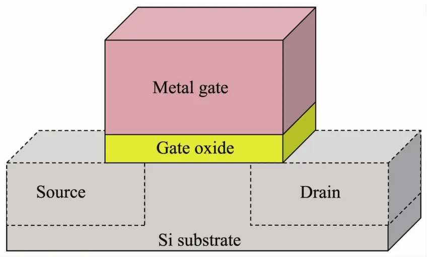
Fig.1 Schematic of a planar transistor in a microelectronic device
To improve the design and decrease current leakage,multigated transistors have been developed in the past few years.One example of such a multigated transistor is a finFET shown in Fig.2[6].FinFETs have a silicon substrate containing a “fin” (a pillar above the substrate).They perform better with less current leakage and higher power output than planar transistors[3,7].Since these structures are more vertical,the surface area increases and more transistors can fit on a chip.Many companies such as Intel,TMSC(Taiwan SemiconductorManufacturing Company),SamsungandIBM haveadopted themultigated transistors such as the tri-gate[3,7-8]. The tri-gate transistor is a finFET where the metal gate layer covers multiple fins.In 2011,Intel announced the 22 nm Ivy Bridge microprocessor,which was the first to use the tri-gate transistor[7-8].Currently,tri-gate and finFET transistors have been used in 14 nm processors by Intel, in their Broadwell-Y processor[9],and Samsung,in their Exynos 7 Octa processor[10].Several companies[11-13],including Samsung[11],Intel[12],TSMC[13],have announced that a 10 nm processor has been fabricated.It has been reported that IBM,working with scientists at SUNY (State Universities of New York)Polytechnic Institute′s Colleges of Nanoscale Science and Engineering,have produced the industry′s first 7 nm node test chips with functional transistors,and TSMC has made progress in 7 nm finFET technology[14-15].IBM announced in June 2017 that it had made the first 5 nm chip in the world through collaboration with Samsung and GlobalFoundries[16].The breakthrough was achieved in part due to the use of both a new gateall-around transistor (GAAFET)with stacks of silicon nanosheets and extreme ultraviolet lithography[17].It should be noted that the cited sources here are either news or reports of the companies in this rapidly changing field.
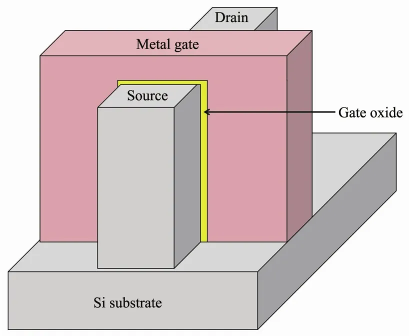
Fig.2 Schematic of a finFET transistor used in a multigate device
Along with the design,new precursor compounds are needed in order to continually improve these transistors.An important constituent in these transistors is the gate oxide layer.Transition metal complexes have been used to fabricate this layer.Ligands in these complexes help tailor characteristics such as shape,reactivity and electronic tunability.Until recently,SiO2was used as the primary gate oxide film.SiO2,however,has a small dielectric constant (k)of 3.9,and is thus not a very good insulating material.As the film gets thinner in the recent transistors,current leakage becomes larger and more significant,generating heat and wasting energy.In addition,the transistors tend to degrade under the heat.Because of the high current leakage,there is a limit to the thickness of the SiO2layer before it becomes too thin and inefficient as an insulating layer[1-2,5,18-23].Due to the decreasing efficiency of SiO2in the new generations of devices,search for new gate oxides started over 25 years ago in order to keep pace with Moore′s law.Gate oxides with high k values are a key to allowing a large number of transistors on each integrated circuit.Table 1 lists common metal oxides and their dielectric constants[19].
In addition to a large k value,the oxide layer needs to meet a few other qualifications before being used in microelectronic devices.One key aspect for a good insulating layer is that the gate oxide has a good interface with the Si substrate beneath it with little to no leaching.Since SiO2contains Si itself,it interfaces well with the Si substrate.Many potentially good oxides,such as Ta2O5,have relatively unstable contacts with Si.Studies of various gate oxides showed that high purity HfO2is one of the few with good thermal stability and interface with the Si substrate.HfO2has shown better electrical performance and film quality as well[24].The introduction of HfO2(k=25)as a gate dielectric material in 2007 by Intel and IBM has allowed the continued shrinking of transistor sizes by making these gate oxide layers thinner and more efficient,as demonstrated in Fig.3[25].
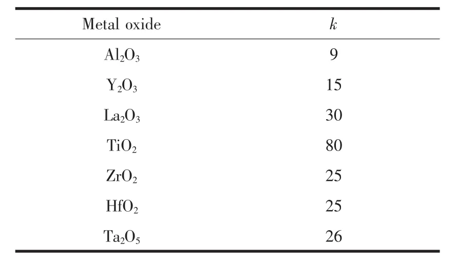
Table 1 List of metal oxides and their dielectric constants[19]
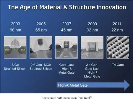
Fig.3 Decrease of transistor size over time;Introduction of high-k metal gate (oxides)in 2007 was considered a milestone event[25]
Reactions of inorganic complexes with oxygen sources such as O2,H2O or O3have been employed to produce metal oxide thin films through methods such as chemical vapor deposition (CVD)and atomic layer deposition (ALD)[26-33].Both processes are well suited for manufacturing gate oxides due to their ability to give uniform and high purity films.An important factor in the manufacturing of thin films is the type of precursors used.Though CVD and ALD have been successfully used to fabricate thin gate oxides,the pathways that the precursors undergo in these processes are not well understood.Understanding the design of these complexes and their reactions in CVD/ALD may enable the design of better precursors and processes to prepare higher quality transistors in microelectronic devices.In this article,we give an overview of CVD and ALD processes,precursors for the formation of metal oxides through CVD and ALD,and our studies of the pathways in the reactions of O2with d0metal amide complexes.It should be pointed out that this paper is not a comprehensive review of CVD and ALD in making microelectronic metal oxides.Such reviews have been published[34-38].Rather,this overview provides a survey for the general readers in inorganic chemistry.
1 Chemical vapor deposition and atomic layer deposition processes
1.1 Chemical vapor deposition
CVD is the process by which thin films are deposited onto a substrate through chemical reactions[29,39-40].The CVD process has been applied to produce coatings,fibers and powders.Coating is the largest application of CVD[30].These coatings have been used in microelectronic,optoelectronic,mechanical and chemical industries for many years.A few examples of coated materials are metal oxides (e.g.,SiO2),metal nitrides (e.g.,TiN),metal carbides (e.g.,W2C)and elemental metals (e.g.,Al)[29-30,39].Reviews such as those written by Powell and Blocher give an extensive coverage on the history of CVD[31].The first practical use of CVD was making metal depositions to strengthen metal filaments in incandescent light bulbs in the 1880′s[30-31].The first reports of Si deposition by hydrogen reduction of SiCl4were in 1909 and 1927[32-33].This material was used widely in many electrical applications after World War II[29,39]. CVD began to grow in the 1960s as technology progressed,and these materials were beginning to be prepared on an industrial scale[30].Variations of the CVD process have been developed to give different kinds of films depending on the applications.
The CVD process starts when volatile precursors are carried by a diluent gas such as H2to a reaction chamber containing a heated substrate[39,41].Gas phase(Fig.4)or surface reactions follow,producing solid products as thin films on the substrate surface.It should be pointed out that gas phase reactions are often avoided because they may lead to non-uniform films[41].However,there are CVD processes of certain films which,e.g.,require gas phase reactions to produce rate-determining intermediates.These reactive intermediates then react with other precursors on the substrate surface[42].In the CVD based on surface reactions,the precursors react on the substrate surface,forming the product films.Once the product deposits onto the surface as a film,the by-products desorb from the substrate and are carried away from the reaction chamber via the carrier gas.CVD is a continuous process as more precursor is introduced into the reaction chamber[5,39,43-44].

Fig.4 Simplified schematic of the CVD process involving gas-phase reactions,In many other CVD processes,precursors react directly on the substrate surface
Film growth depends on several factors including the temperature,pressure and precursors used in the CVD process.At lower temperatures,the rate of film growth is dependent on the reactions of the precursors in the gas phase and on the substrate surface.The growth rate at low temperatures increases exponential-ly when temperature increases.At moderate temperatures,growth rate becomes nearly independent of temperature and becomes more dependent on the mass transport of the precursor to the substrate.At higher temperatures,there is a decrease in film growth due to desorption of precursor molecules from the substrate matrix itself.Gas-phase side reactions also occur,decreasing the amount of precursors deposited onto the substrate[29-30,39].
There are several types of CVD processes,including atmospheric-pressure CVD (APCVD),lowpressureCVD (LPCVD),plasma-enhancedCVD(PECVD)and liquid injection CVD (LI-CVD).The lower pressures in LPCVD aid in the reduction of unwanted side reactions.In PECVD,plasma is used to heat the precursors,making them into free radicals,but the substrate itself is kept at a lower,sometimes ambient temperature.Thus,PECVD allows substrates(such as Al)with a lower melting point to be used in the process[29-30,39].When the precursors are organometallic,the CVD processes are termed metalorganic chemical vapor deposition (MOCVD).Many organometallic precursors are solids,and getting them to the vapor phase is often challenging.In such cases,the precursors may be dissolved in a solvent,injected into an inlet to be volatilized,and carried to the CVD chamber.This process is called liquid injection CVD(LI-CVD).Precursors that are not suitable for other CVD processes may be used to fabricate thin films via LI-CVD[35,39].
In CVD processes,precursors play a very important role and must have certain characteristics.One of the main requirements for a precursor is appropriate volatility for efficient mass transport to the substrate.Gaseous precursors already fulfill this requirement,but many others are liquids or solids.Bulky ligands have been used to control the volatility and stability of the precursors in air.The precursor must also be thermally stable during transport and have a sufficient temperature window between evaporation and decomposition.The precursor needs to be of high purity and have a clean decomposition on the substrate without incorporating impurities in the film or occurrence of side reactions.Good characteristics for precursors are a long shelf life,nontoxic,easy to prepare,inexpensive and stable in air.With these properties,the precursors may be acquired in bulk and stored more easily without decomposition in ambient conditions (i.e.,in air at room temperature)for commercial use.The type of precursors used in CVD depends on the applications of the thin film[30,35,45].
1.2 Atomic layer deposition
Another process to fabricate thin films is ALD via surface exchange reactions[39,46].The first published example,demonstratingtheALD principle (then called “molecular layering”)using surface reactions to coat a substrate,was made by Kol′tsov and Aleskovskii when they coated silica gel with TiO2in the 1960s[47].ALD process was developed further in the 1970s by Suntola et al.to produce ZnS thin films in electroluminescent flat-panel displays[48-49].By the 1980s,this process was used on an industrial scale.One of the primary uses of ALD is to fabricate thin films in microelectronics.As the microelectronics advanced,the interest in ALD increased.The HfO2gate oxide used by Intel® in 2007 was fabricated by ALD[23].
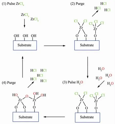
Fig.5 Deposition of ZrO2on a substrate using pulses of ZrCl4 (Step 1)and H2O (Step 3),each followed by inert gas purging (Steps 2 and 4)
ALD occurs in a stepwise process (Fig.5).A pre-cursor is pulsed into the reaction chamber and reacts with the surface OH groups of the substrate forming a monolayer and a by-product.By-products and unreacted precursor are purged from the reaction chamber using an inert gas.A second precursor or co-reagent such as H2O is pulsed into the reaction chamber and reacts with the first monolayer forming a second layer.The chamber then undergoes another purge cycle.Subsequent pulse and purge cycles produce each layer until the desired thickness is achieved[37,39,46,50].
Film growth in an ALD process is self-limiting,i.e.,the amount of material deposited during each cycle is constant.Through this process,the thickness,uniformity and conformity are easily controlled.Besides precise control of the film thickness,ALD has the advantage of having little to no gas-phase reactions as the precursors and co-reagents react directly with surface groups.This aspect allows for more highly reactive precursors to be used for this process[39,46].
ALD process has some disadvantages and limitations.In any process,there may be deviations from the ideal behavior.The film growth is usually less than one monolayer because of steric hindrances in many precursors or limited reactive sites.At higher deposition temperatures,precursors can thermally decompose before being deposited on the substrate.Another major disadvantage is that it has a low effective deposition rate.To be efficient in industry,a process needs to be quick and clean.One method to increase the deposition rate is to shorten the time of each cycle,including,e.g.,the purge or cleaning time such as the ascendant space ALD process.In such cases,there may not be a full coverage of the precursors onto the substrate surface[51].
Precursors are key components in ALD as they are in CVD.The precursors used in ALD have many of the same requirements as precursors used in CVD.The precursors need to be volatile and of high purity.Additionally,they must react quickly and completely with surface groups of the substrate as well as with the co-reagent.The precursors and co-reagents also must be thermally stable so that they will not decompose before or after reacting with the substrate.ALD is usually carried out at 200~300 ℃,which is lower than the thermal decomposition temperature for most precursors.Since there are reactivity requirements between precursors and co-reagents,there are fewer precursors for ALD than for CVD[35-37,44-45,50].
2 Precursors for CVD and ALD processes
Major types of transition metal compounds as precursors in CVD/ALD of metal oxides are discussed here.
2.1 Metal halides and nitrates
Metal halides,such as ZrCl4and TaCl5,were one of the first classes of inorganic precursors in CVD/ALD processes[34,37,45,50].When reacting with H2O,an acid (HX,X=halide)is released as a by-product along with the respective metal oxide,MOn.Metal halides may not be desirable because they have high sublimation temperatures and are corrosive,producing the acid.Also,residual chloride often remains as an impurity in the MOnfilm.It should be noted that metal halides are fairly inexpensive,abundant and easily purified.
Metal nitrates,e.g.,Zr(NO3)4and Hf(NO3)4,have also been used as precursors for the deposition of its respective metal oxide.They are prepared by the reaction of,e.g.,MCl4,with N2O5and purified by sublimation.These inorganic compounds contain no carbon,halogen or hydrogen atoms,thus potentially limiting impurities in the films[52].
To overcome the challenges in using these inorganic compounds,the introduction of organic ligands may give better precursors.This is discussed below.
2.2 Metal alkoxides and amides
Metal alkoxides M(OR)nand amides M(NR2)n(R=alkyl)have also been used in CVD/ALD to fabricate metal oxide films.These halogen-free precursors have been engineered to be better candidates for CVD or ALD processes because the respective halogenated acid is not produced.
When replacing a halide ligand by an alkoxide or amide ligand,the precursor usually becomes more volatile.However,a drawback is the decomposition temperature may be too low,and this could lead to several side reactions resulting in an impure film[34-35,37-38,45,53-55].Cho et al.have deposited HfO2films from Hf(OtBu)4and ozone using ALD (Scheme 1)[56].Hf(NMe2)4is a common precursor for both CVD/ALD processes using O2(Scheme 2)or H2O as the oxygen source[38].It is easily prepared through the reaction of HfCl4with LiNMe2and purified by sublimation.Metal amides react readily with water by the release of amines or with O2by insertion into the M-N bonds[53].Derivatives of metal amides such as Hf(NMeEt)4have been employed in CVD/ALD processes and are commercially available.Gordon et al.have found that the maximum ALD deposition temperature for Hf(NMeEt)4with H2O was 400 ℃.Under these conditions,the amount of carbon and nitrogen was less than 1%and 0.25%,respectively.Another class of amides as precursors are M(NMeNMe2)4(M=Zr,Hf).Hoffman et al.have studied the reactions of M(NMeNMe2)4with O2in which zirconium and hafnium oxide filmswere deposited using low-pressure CVD[54].They have also prepared a hafnium oxide film from the reaction of a bidentate bisamide hafnium complex Hf[tBuNCH2CH2NtBu]2and O2[54].

Scheme 1 Reaction of a hafnium alkoxide with O3[56]

Scheme 2 Reaction of a hafnium amide with O2[38]
Another approach in designing suitable precursors is incorporating oxygen atoms into the starting material.McElwee-White et al.have designed a partially flurorinated oxo-alkoxide tungsten complex[WO(OC(CH3)(CF3)2][57].This volatile complex was used to grow WOxnanorods without an oxygen source.
2.3 Metal amidinates and guanidinates
Conjugated amidinates [RNC(R)NR]-and guanidinates [RNC (NR2)NR]-(R=alkyl)have three bonding modes (Fig.6).A is the most common and the ligand binds to the metal center in a bidentate fashion(Fig.6A).In B,the ligand acts a bridge between two metal atoms.In C,the ligand is monodentate and only a few examples are reported in the literature[58].Amidinates and guanidinates are used as chelating ligands(Fig.6A)to saturate the metal center.This results in more stable monomeric complexes[59].Modification of the alkyl groups on the ligands allows the tuning of their steric requirements[58].However,bulkier R groups often reduce their volatility in comparison to,e.g.,amide ligands (NR2)which may help control the thickness of a metal oxide film.Both volatile metal amides M(NR2)nand less volatile metal amidinates and guanidinates have been used extensively in producing inorganic metal films[34-35]. Devi et al.have studied an amide guanidinate hafnium complex in Scheme 3 with O2[60].They have grown HfO2films (2 and 20 nm thick)on a siliconsubstrateusingLI-CVD (Scheme3)[60].
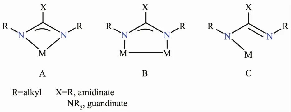
Fig.6 Common coordination modes of amidinate and guanidinate ligands
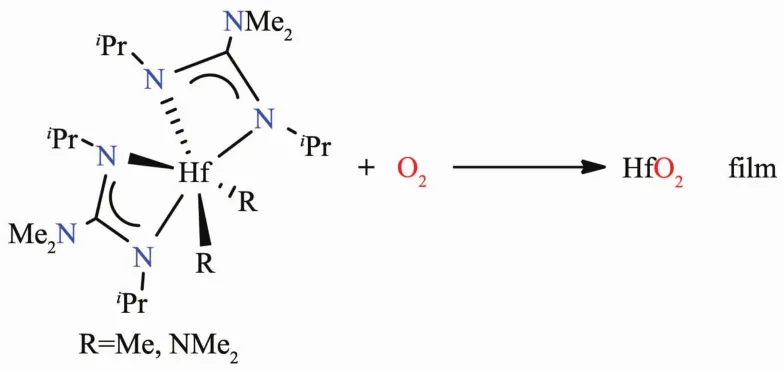
Scheme 3 Reactions of hafnium complexes with O2[60]
Several tantalum amidinate imdo complexes have been synthesized by Winter[61]et al. They have demonstrated the volatility of these tantalum complexes by sublimation and the thermal stability of the complexes by the decomposition temperatures.These compounds were shown to be good candidates for CVD/ALD processes,but they were not subjected to the reactions with an oxygen source.
Tinant et al.have made an amide amidinate chloro hafnium precursor.They have reacted it with isopropyl alcohol and shown that the reaction is selective towards the amide ligand (Scheme 4)[62].The authors have demonstrated that this volatile Hf complex could react selectively towards-OH species,making it an applicable precursor for HfO2films.

Scheme 4 Reaction of an amide amidinate chloro hafnium complex withiPrOH[62]
3 Reactions of d0Groups 4 and 5 complexes with O2
The activation of O2by metal complexes has been actively studied.The focus has been on the reactions of O2with mid-to late transition metal complexes containing valence d electrons (dn).Thus,these reactions often involve metal oxidation.Many precursors, such as Hf(NR2)4(R=alkyl)and the amide guanidinate hafnium in Scheme 3,are d0complexes.They are thus expected to follow different pathways in their reactions with O2since the metals are already at their highest oxidation state.We are primarily interested in the reactions of d0transition metal complexes with O2[63-72]because their pathways to the formation of MOnare not well understood.Since O2is a radical in nature,several pathways may be possible.Our group has focused on the reactions of O2with d0Groups 4 and 5 amides and Group 4 amidinate and guanidinate complexes[63-72].
Wefirststudied thereactionsofGroup 4 homoleptic amides M(NMe2)4(M=Zr,Hf)with O2,yielding oxo aminoxides M3(NMe2)6(μ-NMe2)3(μ3-O)(μ3-ONMe2)and byproduct Me2NNMe2(Scheme 5)[64].The results suggest there are two important steps in the reactions of M(NMe2)4with diradical ∶O2(a)O insertion into M-N bonds,forming aminoxy ligands; (b)Cleavage of the O-N bond in the O-NMe2ligands to yield the oxo ligands in the products.These are rare chances to observe formations of the ligands and the elementary steps in the formation of metal oxides from the reactions of d0metal amides with O2.
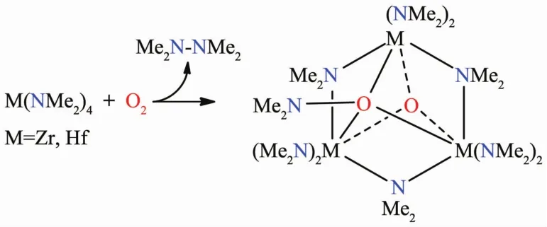
Scheme 5 Reactions of Group 4 amides with O2[64]
Reactions of M(NR2)5(M=Nb,Ta;R=Me,Et)with O2have also been studied and the isolated products are shown in Scheme 6[65-66].DFT studies of the reactions between Ta(NMe2)5and O2indicate that one key step is the insertion of O2into an M-N bond to give the peroxide complex (Me2N)4Ta(η2-O-O-NMe2)[66].The peroxide ligand then either oxidizes an amide to an imine ligand (Me-N=CH2)through the abstraction of a hydride or inserts its atom into another Ta-NMe2bond,forming (Me2N)3Ta(η2-ONMe2)2.Insertion of Me-N=CH into a Ta-NMe2bond yields the unusual-N(Me)CH2NMe2ligand in the products.
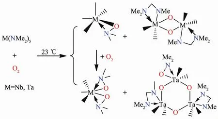
Scheme 6 Reactions of Group 5 amides with O2[65-66]
These homoleptic amides are very reactive.Their reactions occur at room temperature or a lower temperature,which may pose a problem in the CVD/ALD processes because several side reactions may occur.To reduce the reactivity,bidentate,N-containing ligands have been introduced to help control reaction conditions.We have studied the reactions of O2with two different types of Zr bidentate complexes:Zr amide amidinates[70]and Zr amide guanidinates[72].
Reaction of the amide amidinate Zr(NMe2)2[MeC(NiPr)2]2(1)with O2affords three Zr species:peroxo trimer{(μ-η2∶η2-O2)Zr[MeC (NiPr)2]2}3(2),oxo dimer{(μ-O)Zr[MeC(NiPr)2]2}2(3),and an insoluble polymer{(μ-O)Zr[MeC(NiPr)2]2}n(4)(Scheme 7)[71].Peroxo trimer 2 was characterized by single-crystal X-ray diffraction.Peroxo dimer{(μ-η2∶η2-O2)Zr[MeC (NiPr)2]2}2was observed in the gas phase by mass spectroscopy.To our knowledge,this was the first observed peroxo species from the reaction of O2with a d0complex without a redox active ligand.It should be noted that a peroxo species has not been observed in any other reactions of d0metal amides with O2[64-70,72].The peroxo complex 2 is very reactive.In the presence of starting material 1,2 quickly reacts with 1,forming the oxo products 3 and 4.

Scheme 7 Reaction of Zr(NMe2)2[MeC(NiPr)2]2 (1)with O2and crystal structure of the Zr peroxo trimer 2[71]
4 Perspectives
As transistors continue to shrink in size in microelectronic devices,the metal gate oxide layer in the transistors also needs to reduce in size.SiO2alone is no longer adequate for today′s devices.To meet this challenge,new precursors have been prepared for the fabrication of metal oxide thin films by CVD or ALD.Tuning the characteristics of the complexes by using different metal centers and various ligands leads to a diverse pool of precursors.
One important challenge is determining the pathways of the reactions between the metal complexes and O2.Our recent work has contributed to the understanding of the pathways.
The size of the transistors is projected to keep shrinking over the next decade (Fig.6)[25].Si-based microelectronic devices may not be adequate in the near future.As shown in Fig.6,we may soon enter into the post-Si era.The Materials Research Society has published a bulletin containing several articles on new,post-Si materials,including Ge and Group III-V semiconductors such as GaAs[73].Many of these materials contain more than one metal or metalloid (e.g.,GeSnOx)that are expected to improve the performance of the transistors.Integration of these materials onto the transistors is challenging.Binding to the substrate,usually made of Si,without leaching or degrading of the materials over time is a key issue and an active area of current research.
Another direction to develop transistors is incorporating organic semiconductors on plastic substrates or metal oxides to make them flexible[74-76].These new organic-inorganic hybrid materials are made through solution-based film growth processes.By incorporating the inorganic component,the transistors maintain a high k value while the organic component makes the material more flexible.Unlike CVD or ALD,this process does not require high temperatures or expensive vacuum deposition technologies.
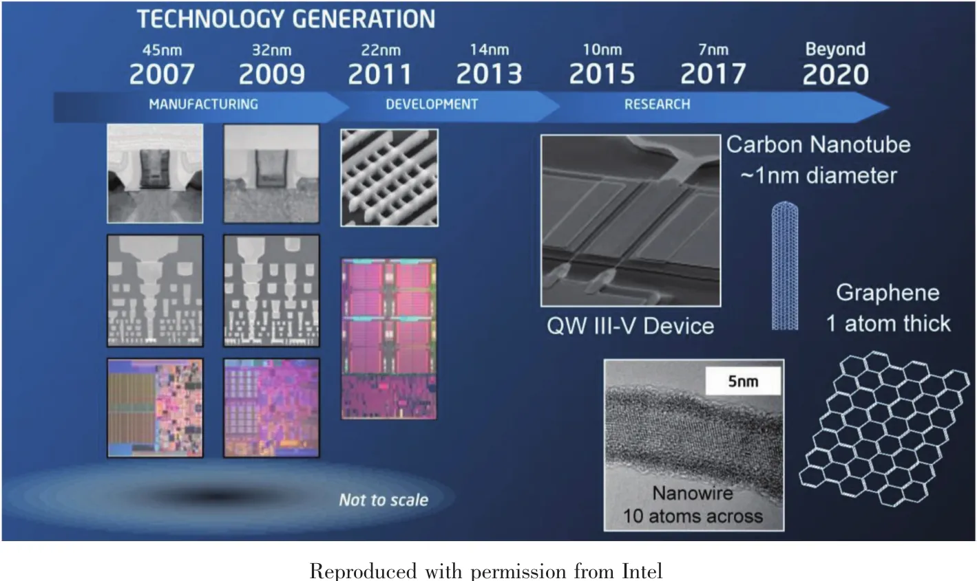
Fig.7 Development and future projection of the transistor size[25]
Graphene,as well as graphene-based derivatives,have been considered for use in dielectric materials because of their interesting electronic properties[25,77-82].Graphene is a flexible polymer of sp2-hybridized carbon atoms arranged in a flat lattice and can be deposited onto surfaces via CVD,making each monolayer 1 atom thick or 0.34 nm[81].Using this material along with a metal oxide film as the gate layer would decrease the size of transistors.Graphene has been shown to enhance the dielectric constant when used as an interlayer between polymer layers to form a flexible dielectric film[79].Graphene oxide and reduced graphene oxide have been used as dielectric materials in graphene oxide-based FET[80].
At present,designing new transistors is complex and costly.Depending on the transistor′s application,one fabrication process may be better than another.Research is being conducted to explore the properties of new organic and/or inorganic materials as the gate oxides.These advances are projected over the next decade[25].
[1]Rockett A.The Materials Science of Semiconductors.New York:Springer,2008.
[2]Robertson J.Rep.Prog.Phys.,2006,69:327-396
[3]Jan C.H.ECS Trans.,2012,44(1):451-470
[4]Ytterdal T,Cheng Y,Fjeldly T A.Device Modeling for Analog and RF CMOS Circuit Design.Chichester:Wiley,2003:1-45
[5]Sah C H.Fundamentals of Solid-State Electronics.Singapore:World Scientific Publishing Co.,1991:521-694
[6]Hisamoto D,Lee W C,Kedzierski J,et al.IEEE Trans.Electron Devices,2000,47(12):2320-2325
[7]https://www.intel.se/content/dam/www/public/us/en/documents/presentation/revolutionary-22nm-transistor-technologypresentation.pdf
[8]https://newsroom.intel.com/news-releases/intel-reinventstransistors-using-new-3-d-structure/
[9]http://www.intel.com/content/www/us/en/silicon-innovations/advancing-moores-law-in-2014-presentation.html
[10]https://news.samsung.com/global/samsung-announces-massproduction-of-2nd-generation-14-nanometer-finfet-logic-process-technology
[11]http://www.samsung.com/semiconductor/about-us/news/25881/samsung-starts-industry-first-mass-production-of-soc-with-10-nan-finfet-technology
[12]http://spectrum.ieee.org/semiconductors/devices/intel-findsmoores-laws-next-step-at-10-nanometers
[13]http://wccftech.com/tsmc-promises-10nm-production-2016-7 nm-2017/
[14]https://www.flickr.com/photos/ibm_research_zurich/18876220 214/in/album-72157655342048792/
[15]http://www.tsmc.com/download/ir/annualReports/2016/english/e_2_2.html
[16]https://www-03.ibm.com/press/us/en/pressrelease/52531.wss
[17]https://arstechnica.com/gadgets/b2017/06/ibm-5nm-chip/?comments=1
[18]Smith R C,Ma T,Hoilien N,et al.Adv.Mater.Opt.Electron.,2000,10(3/4/5):105-114
[19]Wallace R,Wilk G D.Crit.Rev.Solid State Mater.Sci.,2003,28(4):231-285
[20]Wilk G D,Wallace R M,Anthony J M.J.Appl.Phys.,2001,89(10):5243-5275
[21]Arghavani R,Miner G,Agustin M.Semicond.Int.,2007,30(12):32-34,36,38
[22]Jones A C,Aspinall H C,Chalker P R,et al.J.Mater.Chem.,2004,14(21):3101-3112
[23]Walawalkar M G,Kottantharayil A,Rao R.Synth.React.Inorg.Met.-Org.Nano-Met.Chem.,2009,39(6):331-340
[24]Wallace T,Wilk G.MRS Bull.,2002,27(3):192-197
[25]https://nanohub.org/resources/20880
[26]Thin Film Processes Ⅱ.Vossen J L,Kern W,Ed.,San Diego:Academic Press,1991.
[27]Campbell S A.Science and Engineering of Microelectronic Fabrication.2nd Ed.Oxford:Oxford University Press,2001.[28]Panda D,Tseng T Y.Thin Solid Films,2013,531:1-20
[29]Hitchman M L,Jensen K F.Chemical Vapour Deposition:Principles and Applications.London:Academic Press,1993:1-90
[30]Pierson H O.Handbook of Chemical Vapor Deposition:Principles,Technology,and Applications.Park Ridge,New Jersey:Noyes Publications,1992.
[31]Powell C F,Oxley J H,Blocher J M et al.Vapor Deposition.New York:The Electrochemical Society,1966.
[32]Pring J N,Fielding W.J.Chem.Soc.,1909,95:1497-1506
[33]Holbling R.Z.Angew.Chem.,1927,40:655-659
[34]Jones A C,Aspinall H C,Chalker P R.Chemical Vapour Deposition:Precursors,Processes and Applications.Jones A C,Hitchman M C.Ed.,Cambridge,UK:Royal Society of Chemistry,2009:357-412
[35]Devi A.Coord.Chem.Rev.,2013,257:3332-3384
[36]Emslie D J H,Chadha P,Price J S.Coord.Chem.Rev.,2013,257(23/24):3282-3296
[37]Leskela M,Ritala M.Thin Solid Films,2002,409(1):138-146
[38]Choi J H,Mao Y,Chang J P.Mater.Sci.Eng.R,2011,72(6):97-136
[39]Jones A C,Hitchman M C.Chemical Vapour Deposition:Precursors,Processes and Applications.Jones A C,Hitchman M C.Ed.,Cambridge,UK:Royal Society of Chemistry,2009:1-36
[40]http://www.pob.manchester.ac.uk/research.html
[41]Handbook of Nanophase and Nanostructured Materials.Boston:Springer,2003:102-144
[42]Chae Y K,Shimogaki Y,Komiyama H.Electrochem.Soc.,1998,145(12):4226-4233
[43]Allendorf M D,Besmann T M,Kee R J,et al.Chemical Vapour Deposition:Precursors,Processes and Applications.Jones A C,Hitchman M C.Ed.,Cambridge,UK:Royal Society of Chemistry,2009:93-157
[44]Thompson A G.Mater.Lett.,1997,30:255-263
[45]Malik M A,O′Brien P.Chemical Vapour Deposition:Precursors,Processes and Applications.Jones A C,Hitchman M C.Ed.,Cambridge,UK:Royal Society of Chemistry,2009:207-271
[46]Ritala M,Niinisö J.Chemical Vapour Deposition:Precursors,Processes and Applications.Jones A C,Hitchman M C.Ed.,Cambridge,UK:Royal Society of Chemistry,2009:158-205
[47]Kol′tsov S I,Aleskovskii V B.Russ.J.Phys.Chem.,1968,42:630-632
[48]Suntola T,Hyvrinen J.Annu.Rev.Mater.Sci.,1985,15:177-195
[49]Parsons G N,Elam J W,George S M,et al.J.Vac.Sci.Technol.A,2013,31(5):050818(11 pages)
[50]Tauber R N,Dumbri A C,Caffrey R E.J.Electrochem.Soc.,1971,118(5):747-754
[51]Poodt P,Lankhorst A,Roozeboom F,et al.Adv.Mater.,2010,22(32):3564-3567
[52]Smith R C,Ma T,Hoilien N,et al.Adv.Mater.Opt.Electron.,2000,10(3/4/5):105-114
[53]Hausmann D M,Kim E,Becker J,et al.Chem.Mater.,2002,14(10):4350-4358
[54]Lehn J S M,Javed S,Hoffman D M.Chem.Vap.Deposition,2006,12(5):280-284
[55]Hausmann D M,de Rouffignac P,Smith A,et al.Thin Solid Films,2003,443(1/2):1-4
[56]Chang H S,Baek S K,Park H,et al.Electrochem.Solid-State Lett.,2004,7(6):F42-F44
[57]Bonsu R O,Kim H,O′Donohue C,et al.Dalton Trans.,2014,43(24):9226-9233
[58]Edelmann F T.Adv.Organomet.Chem.,2013,61:55-374
[59]Xu K,Milanov A P,Winter M,et al.Eur.J.Inorg.Chem.,2010(11):1679-1688
[60]Thomas R,Rije E,Ehrhart P,et al.J.Electrochem.Soc.,2007,154(3):G77-G84
[61]Wiedmann M K,Heeg M J,Winter C H.Inorg.Chem.,2009,48(12):5382-5391
[62]Eleter M,Hubert-Pfalzgraf L G,Daniele S,et al.Polyhedron,2010,29(12):2522-2526
[63]Chen S J,Zhang X H,Lin Z,et al.Sci.China Chem.,2009,52(11):1723-1733
[64]Wang R,Zhang X H,Chen S J,et al.J.Am.Chem.Soc.,2005,127(14):5204-5211
[65]Chen S J,Zhang J,Yu X,et al.Inorg.Chem.,2010,49(9):4017-4022
[66]Chen S H,Zhang X H,Yu X,et al.J.Am.Chem.Soc.,2007,129(46):14408-14421
[67]Woods J B,Beach D B,Nygren C L,et al.Chem.Vap.Deposition,2005,11(6/7):289-291
[68]Chen T N,Zhang X H,Wang C S,et al.Organometallics,2005,24(6):1214-1224
[69]Chen T N,Wu Z Z,Li L T.J.Am.Chem.Soc.,1998,120(51):13519-13520
[70]Morton L A,Miao M,Callaway T M,et al.Chem.Commun.,2013,49(83):9555-9557
[71]Lamb A C,Lu Z,Xue Z L.Chem.Commun.,2014,50(72):10517-10520
[72]Sharma B,Callaway T M,Lamb A C,et al.Inorg.Chem.,2013,52(19):11409-11421
[73]Liu C W,Östling M,Hannon J B.MRS Bull.,2014,39(8):658-726
[74]Ha Y G,Everaerts K,Hersam M C,et al.Acc.Chem.Res.,2014,47(4):1019-1028
[75]Ting G G,Acton O,Ma H,et al.Langmuir,2009,25(4):2140-2147
[76]Ha Y G,Emery J D,Bedzyk M J,et al.J.Am.Chem.Soc.,2011,133(26):10239-10250
[77]Geim A K.Science,2009,324(5934):1530-1534
[78]Castro Neto A H,Guinea F,Peres N M R,et al.Rev.Mod.Phys.,2009,81(1):109-162
[79]Kim J Y,Lee J,Lee W H,et al.ACS Nano,2014,8(1):269-274
[80]Eda G,Nathan A,Wöbkenberg P,et al.Appl.Phys.Lett.,2013,102(13):133108(4 pages)
[81]Avouris P,Farmer D B,Lin Y M,et al.US Patent,8344358.2013-01-01.
[82]http://www.screen.co.jp/eng/spe/mt-images/5_ASML.pdf
Metal Oxides and Modern Microelectronics:Roles of Transition Metal Compounds and their Conversion to the Materials
Tabitha M.Cook Adam C.Lamb XUE Zi-Ling*
(Department of Chemistry,The University of Tennessee,Knoxville,Tennessee 37996,USA)
Thin films of metal oxides such as HfO2[known as high k dielectrics (or metal gate)]are a key component of modern microelectronic devices in computers (tablet,laptop and desktop),smartphones,smart TVs,automobiles and medical devices.The metal oxides,with large dielectric constants (k),have replaced SiO2that has a small k of 3.9,thus making it possible to further miniaturize microelectronic components.Transition metal complexes have been widely used as precursors to produce thin films through their reactions with O2,H2O or O3in chemical vapor deposition (CVD)and atomic layer deposition (ALD)processes.The microelectronic metal oxide films are one of the most widely used nano materials.Recent progresses,including our studies of the reactions of d0transition metal complexes with O2,are overviewed.
metal oxides;gate dielectrics;thin films;microelectronics;CVD;ALD
O614
A
1001-4861(2017)11-1947-12
10.11862/CJIC.2017.249
2017-07-26。收修改稿日期:2017-09-22。
美国国家科学基金会(No.CHE-1633870)资助项目。
*通信联系人。E-mail:xue@utk.edu

