Efficient Perovskite-organic Bulk Heterojunction Hybrid Integrated Solar Cells
2015-07-21 15:45TANGTongZUOHongwenWANGYalingQINWenjingCAOHuanqiYANGLiyingYAOCongGEZiyiYINShougen
发光学报 2015年9期
TANG Tong,ZUO Hong-wen,WANG Ya-ling,QINWen-jing, CAO Huan-qi,YANG Li-ying*,YAO Cong,GE Zi-yi,YIN Shou-gen*
(1.Key Laboratory ofDisplay Materials and Photoelectric Devices,Education Ministry ofChina, School ofMaterials Science and Engineering,Tianjin University of Technology,Tianjin 300384,China; 2.Tianjin Key Laboratory for Photoelectric Materials and Devices,Tianjin University ofTechnology,Tianjin 300384,China; 3.China Electronics Technology Group Corporation No.18th Research Institute,Tianjin 300384,China; 4.Ningbo Institute ofMaterials Technology&Engineering,Chinese Academy of Sciences,Ningbo 315201,China) *Corresponding Author,E-mail:liyingyang@tjut.edu.cn
Efficient Perovskite-organic Bulk Heterojunction Hybrid Integrated Solar Cells
TANG Tong1,2,ZUO Hong-wen1,2,WANG Ya-ling1,2,QINWen-jing1,2, CAO Huan-qi1,2,YANG Li-ying1,2*,YAO Cong3*,GE Zi-yi4*,YIN Shou-gen1,2*
(1.Key Laboratory ofDisplay Materials and Photoelectric Devices,Education Ministry ofChina, School ofMaterials Science and Engineering,Tianjin University of Technology,Tianjin 300384,China; 2.Tianjin Key Laboratory for Photoelectric Materials and Devices,Tianjin University ofTechnology,Tianjin 300384,China; 3.China Electronics Technology Group Corporation No.18th Research Institute,Tianjin 300384,China; 4.Ningbo Institute ofMaterials Technology&Engineering,Chinese Academy of Sciences,Ningbo 315201,China) *Corresponding Author,E-mail:liyingyang@tjut.edu.cn
An integrated perovskite/organic bulk-heterojunction(BHJ)photovoltaic device was fabricated for efficient lightharvesting and energy conversion.The structure of the solar cells consists of two photovoltaic layers,namely a methylammonium lead iodide(CH3NH3PbI3)and poly(3-hexylthiophene)(P3HT)blended with methanofullerene[6,6]-phenyl C61-butyric acid methyl ester(PCBM)organic BHJactive layer.The power conversion efficiency(PCE)of6.54%was achieved in the integrated devicewith a Jscof19.14 mA/cm2,a Vocof0.76 V,and a FF of 45.0%.Compared to that of CH3NH3PbI3/PCBM planar device,the enhanced performance indicates that the BHJ film absorbs light and contributes to the current density of the device.Our research further demonstrates the compatibility and synergistic potential of the perovskite and organic bulk-heterojunction(BHJ)photovoltaic device.
perovskite;bulk heterojunction;integrated solar cells
1 Introduction
The ever increasing world energy consumption entails the depletion of fossil energy resources.Consequently,people are facing a growing quest for the development of low-cost renewable energy sources. Solar technology is regarded as the one of the most prominent choice to directly convert renewable energy into electricity using photovoltaic cells.Conventional silicon-based solar cells which permit an efficient conversion of solar energy into electrical power have developed and commercialized many years ago. However,the high purity requirements for the raw materialsmake the fabrication processes and the resulting energy payback time too long and too cost-intensive to impair the deployment of such solar cells on a terawatt scale.During the past three decades, several promising alternatives based on cost-effective materials have been proposed[1-3].Amongst them, organic-inorganic hybrid metal halide perovskites, CH3NH3MX3(M=Pb,Sn;X=halogen),have gained notable attention and shown high performance due to direct band gap,large absorption coefficient, long exciton diffusion lengths and high charge carrier mobility[4-9].The potential advantage of the metal halide perovskite photovoltaic technologies is their use of abundant low-costmaterials that can be processed from solution,enabling the application of large-area printing techniques to reduce the fabrication costs and the energy payback time[10-11].Since the pioneer work by Miyasaka and co-workers in 2009,various device structures ranging from mesoscopic structure to the planar heterojunction architecture have been explored[12-16].To date,through optimizing device design,material interfaces and processing techniques,a certified efficiency of 20.1% has been reported.These recent developments demonstrate the enormous potential of perovskite solar cells,with trajectory suggesting that they should soon compete with traditional silicon solar cells.
In this paper,we demonstrate the fabrication of aperovskite-organic bulk heterojunction hybrid integrated solar cells consisting of two photovoltaic layers, namely amethylammonium lead iodide(CH3NH3PbI3) and poly(3-hexylthiophene)(P3HT)blended with methanofullerene[6,6]-phenyl C61-butyric acid methyl ester(PCBM)organic BHJ active layer. UV-Vis and atomic forcemicroscopy(AFM)measurementswere used to characterize the interface between the perovskite and the organic bulk heterojunction.
2 Experiments
2.1 M aterials
Poly(3-hexylthiophene)(P3HT,4002-E)with purity over 99%was purchased from Rieke Met.Inc. Fullerene derivative(PCBM)with purity over 99% was obtained from Solenne B.V.,Netherlands. PbI2(99.999%)was purchased from Aldrich Co.. An aqueous dispersion of PEDOT:PSS(Baytron®P VP Al 4083)was obtained from Heraeus Co..All the materials were used as received.CH3NH3Iwas synthesized using the same method as published in literature[17].ITO-coated glass with a sheet resistance of 10Ω/□was used for device fabrication. The routine cleaning procedure includes ultra-sonication in a solution of detergent,deionized water, and isopropyl alcohol in sequence.
2.2 Device Fabrication and Performance M easurements
The schematic device structures and the energy level diagrams of each layer are shown in Fig.1. The procedure for the solar cell device fabrication is described as follows.PEDOT:PSS layer of about 40 nm was obtained by spin coating at 3 000 r/min for 30 s on ITO coated glass substrates,followed by baking at 120℃for 30 min in air.For depositing the perovskite layer,first a layer of PbI2was spincoated on top of the PEDOT:PSS-coated ITO substrate from a 1 mol/L DMF solution.After the PbI2film was dried at 70℃in air,CH3NH3Iwas spincoated on top of PbI2layer from an isopropanol solution with a concentration of 38 mg/mL with a spin rate of 1 500 r/min to form the perovskite structure and then annealed at 90℃for 2 h.The blend of P3HT:PCBM(1:0.8 by weight)chlorobenzene solution is spin-coated at 800 r/min for 10 s on the perovskite layer to form a 100 nm thick active layer. Finally,100 nm Al are thermally evaporated under a vacuum of a pressure of 1×10⁻⁴Pa.For comparison,80 nm PCBM(20 mg/mL in o-dichlorobenzene)was then sequentially deposited by spin coating at1 500 r/min for12 s on top of CH3NH3PbI3layer to form control perovskite planar device structure.All the fabrication and characterization procedures were performed in an ambient atmosphere at room temperature.The active layer area of the device is 0.09 cm2defined by a shadow mask.
J-V characteristics of the un-encapsulated devicesweremeasured under intensity of100 mW/cm2illuminations by using a 300 W solar simulator with an AM 1.5 G filter.The light intensity was calibrated with an Orielmono-Si reference cell(CROWNTECH PVM 272 certificated by NREL).The surface roughness and morphology of PEDOT:PSS,PbI2, CH3NH3PbI3,CH3NH3PbI3/PCBM and CH3NH3PbI3/ P3HT:PCBM layers were characterized by Bruker INNOVA AFM in tapping mode.The thickness of above layer was measured by a surface profiler (KLA Tencor Alpha Step D-100).More detailed information on device fabrication and device characterization can be found in our previous paper[18].
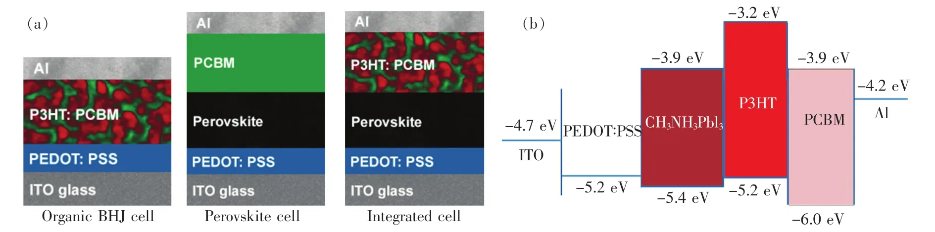
Fig.1 (a)Schematic diagrams of the device structure for organic BHJ cell,perovskite cell and integrated cell.(b)Schematic energy level diagrams of each layer.
3 Results and Discussion
To understand the light absorption property of the integrated solar cells,the absorption spectra for CH3NH3PbI3/PCBM bi-layer film,P3HT:PCBM blend film and CH3NH3PbI3/P3HT:PCBM film weremeasured,as show in Fig.2.The thickness for CH3NH3PbI3film,PCBM film,P3HT:PCBM blend film and CH3NH3PbI3/P3HT:PCBM bi-layer is 260,80,100,360 nm,respectively.The absorption spectrum of the CH3NH3PbI3/P3HT:PCBM film shows a good accumulation of the respective absorption of CH3NH3PbI3film and the P3HT:PCBM BHJ blend film.

Fig.2 Absorption spectra of P3HT:PCBM blend film, CH3 NH3 PbI3/PCBM film and CH3 NH3 PbI3/P3HT: PCBM film,respectively.
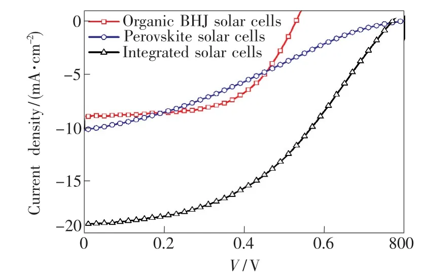
Fig.3 J-V curves for the organic BHJ solar cells,perovskite solar cells,and the integrated solar cells,respectively.
The current density-voltage(J-V)curves of the integrated perovskite/BHJ solar cell,P3HT:PCBM BHJ solar cell as well as the single junction perovskite solar cell are shown in Fig.3.The detailed device performance parameters are summarized in Table 1.As shown in Fig.3 and Table 1,the integrated devices show higher performance than that of the pristine perovskite device due to the increased shortcircuit current(Jsc)and fill factor(FF).The reference perovskite device shows Jsc,open-circuit voltage(Voc),and FF of 10.3 mA/cm2,0.79 V, and 28.3%,respectively,leading to a PCE of 2.27%.The best integrated CH3NH3PbI3/P3HT: PCBM(100 nm)device gives a PCE of 6.54%, with a Jscof19.14mA/cm2,a Vocof0.76 V,and a FF of 45.0%.Accordingly,the improved performancemainly originates from the increased values of Jscand FF at the same time.Jscis higher than that of perovskite cells due to additional photocurrent contribution from the P3HT:PCBM bulk-heterojunction.
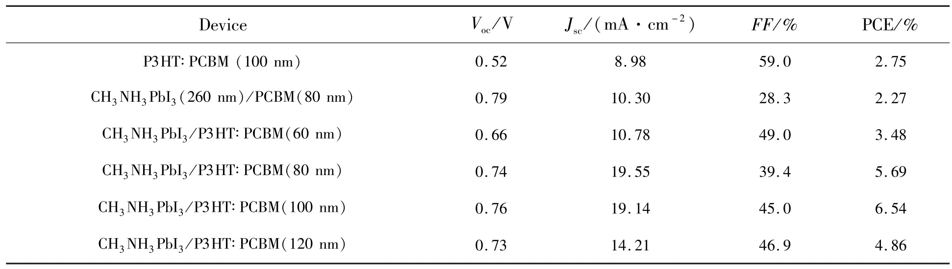
Table 1 Summary of device performances for the organic BHJ solar cells,perovskite solar cells and the integrated solar cells

Fig.4 AFM topographic images of the surfacemorphology of ITO/PEDOT:PSS(a),ITO/PEDOT:PSS/PbI2(b),ITO/PEDOT: PSS/CH3 NH3 PbI3(c),ITO/PEDOT:PSS/CH3 NH3 PbI3/PCBM(d),and ITO/PEDOT:PSS/CH3 NH3 PbI3/P3HT: PCBM(e)films,respectively.
In order to conducta deeper insight into the enhancement in the performance,we investigated the morphology of devices by AFM.Fig.4 shows the AFM images of the surface morphology of PEDOT: PSS,PbI2,CH3NH3PbI3,CH3NH3PbI3/PCBM,and CH3NH3PbI3/P3HT:PCBM films measured over an area of 5μm×5μm.Fig.4(a)shows the topographic images of PEDOT:PSS film spin-coated on the ITO electrode.Raand RMS roughness is 2.47 and 3.11 nm,respectively.The surface of the Pb I2on the PEDOT:PSS film(Fig.4(b))is a rougher morphology with a RMS roughness of 12.5 nm.
Next,we measured the topographic images of the CH3NH3PbI3layer prepared on PEDOT:PSS. RMS roughness is increased to about20.5 nm(Fig. 4(c)),Fig.4(d)and 4(e)display CH3NH3PbI3/ PCBM and CH3NH3PbI3/P3HT:PCBM bi-layer on the surface of ITO/PEDOT:PSS,respectively.The surface of the CH3NH3PbI3/P3HT:PCBM film was smooth than CH3NH3PbI3,with Raand RMS roughness of 13.7 and 17.5 nm,respectively.In contrast, amuch rougher surface with a RMS roughness of 55.4 nm is observed for CH3NH3PbI3/PCBM layer.The surface morphology image indicates that the introduction of P3HT interlayer into a CH3NH3Pb I3/PCBM planar heterojunction device has positive effect on the surface roughness.Consequently,a better charge transport interface is expected to form between CH3NH3PbI3film and P3HT:PCBM organic active layer.As a result, the performance of CH3NH3Pb I3/PCBM planar heterojunction device is improved.Higher photocurrent density and PCE would be expected by further device optimization.Moreover,by applying suitable low band gap high-performance polymers and optimizing perovskite device structure, much higher PCE can bemade.
4 Conclusion
In summary,an integrated solar cell combining a perovskite solar cell and an organic BHJ solar cell is investigated.Compared with the control perovskite planar device structure,the addition of an organic BHJ layer broadens the photoresponse of perovskite solar cell and improves themorphology of the interfacial layer.The best integrated CH3NH3PbI3/P3HT:PCBM device gives a PCE of 6.54%,with a Jscof 19.14 mA/ cm2,a Vocof 0.76 V,and a FF of 45.0%.The improved performance mainly originates from the increased values of Jscand FF at the same time. Therefore,enlarged photoresponse and enhanced photocurrent benefit from bulk heterojunction.By applying suitable low band gap high-performance polymers and optimizing perovskite device structure, much higher PCE can bemade.
[1]Martin A G,Keith E,Yoshihiro H,et al.Solar cell efficiency tables(Version 45)[J].Prog.Photovolt.:Res.Appl., 2015,23(1):1-9.
[2]Wu J,Xie Z Y.Polymer solar cells fabricated with doctor-blade coating technique[J].Chin.J.Lumin.(发光学报), 2012,33(5):540-544(in Chinese).
[3]Yan X M,Wang Q K.Study on application of CdSe/ZnSe/ZnS quantum dots in monocrystalline silicon solar cells[J]. Chin.J.Lumin.(发光学报),2013,34(10):1358-1361(in Chinese).
[4]Kim H S,Lee CR,Im JH,et al.Lead iodide perovskite sensitized all-solid-state submicron thin film mesoscopic solar cell with efficiency exceeding 9%[J].Sci.Rep.,2012,2:591-597.
[5]Lee M M,Teuscher J,Miyasaka T,et al.Efficient hybrid solar cells based on meso-superstructured organometal halide perovskites[J].Science,2012,338:643-647.
[6]Crossland E JW,Noel N,Sivaram V,et al.Mesoporous TiO2single crystals delivering enhanced mobility and optoelectronic device performance[J].Nature,2013,495:215-219.
[7]Heo JH,Im SH,Noh JH,etal.Efficient inorganic-organic hybrid heterojunction solar cells containing perovskite compound and polymeric hole conductors[J].Nat.Photon.,2013,7:486-491.
[8]Burschka J,Pellet N,Moon S J,et al.Sequential deposition as a route to high-performance perovskite-sensitized solar cells[J].Nature,2013,499:316-319.
[9]Xing G H,Mathews N,Sun S Y,et al.Long-range balanced electron and hole-transport lengths in organic-inorganic CH3NH3PbI3[J].Science,2013,342(6156):344-347.
[10]Zhou H P,Chen Q,LiG,et al.Interface engineering of highly efficient perovskite solar cells[J].Science,2014,345 (6196):542-546.
[11]NieW Y,TsaiH,Asadpour R,etal.High-efficiency solution processed perovskite solar cellswithmillimeter scale grains [J].Science,2015,347(6221):522-525.
[12]Shi D,Adinolfi V,Comin R,etal.Low trap-state density and long carrier diffusion in organolead trihalide perovskite single crystals[J].Science,2015,347(6221):519-522.
[13]Dong Q F,Fang Y J,Shao Y C,et al.Electron-hole diffusion lengths>175μm in solution-grown CH3NH3PbI3single crystals[J].Science,2015,347(6225):967-970.
[14]Wu X X,Trinh M T,Niesner D,etal.Trap states in lead iodide perovskites[J].J.Am.Chem.Soc.,2015,137(5):2089-2096.
[15]Kojima A,Teshima K,Shirai Y,et al.Organometal halide perovskites as visible-light sensitizers for photovoltaic cells [J].J.Am.Chem.Soc.,2009,131:6050-6051.
[16]Jeng JY,Chiang Y F,Lee M H,etal.(CH3NH3)PbI3perovskite fullerene planar heterojunction hybrid solar cells[J]. Adv.Mater.,2013,25(27):3727-3732.
[17]Etgar L,Gao P,Xue Z S,et al.Mesoscopic CH3NH3PbI3/TiO2heterojunction solar cells[J].J.Am.Chem.Soc., 2012,134:17396-17399.
[18]Xu X J,Yang L Y,Tian H,et al.Enhanced performance and stability in polymer photovoltaic cells by using ultraviolet treated PEDOT:PSS[J].Chin.Phys.Lett.,2013,30(7):077201-1-5.

唐彤(1990-),男,湖南宁乡人,硕士研究生,2012年于湖南师范大学获得学士学位,主要从事有机光电材料与器件的研究。
E-mail:qingyi5173@163.com

杨利营(1973-),男,河北石家庄人,研究员,2002年于天津大学获得博士学位,主要从事有机光电功能材料与器件的研究。
E-mail:liyingyang@tjut.edu.cn
高效钙钛矿-有机本体异质结杂化串联太阳能电池
唐 彤1,2,左红文1,2,王亚凌1,2,秦文静1,2,曹焕奇1,2,杨利营1,2*,姚 聪3*,葛子义4*,印寿根1,2*
(1.天津理工大学显示材料与光电器件教育部重点实验室,天津 300384; 2.天津理工大学天津市光电显示材料与器件重点实验室,天津 300384; 3.中国电子科技集团第18研究所,天津 300384; 4.中国科学院宁波材料所,浙江宁波 315201)
制备了一种有机铅卤钙钛矿-有机本体异质结杂化串联太阳能电池。采用紫外可见吸收光谱、原子力显微镜对薄膜形貌进行了表征。结果表明:有机本体异质结层可以有效改善钙钛矿的表面形貌,增强了可见光的吸收。优化后的串联结构电池的短路电流可达19.14 mA/cm2,开路电压为0.76 V,光电转换效率达到了6.54%。钙钛矿电池和有机本体异质结电池串联结构可以同时提高短路电流及填充因子,二者具有较好的相容性和协同作用。
钙钛矿;本体异质结;串联电池
1000-7032(2015)09-1047-06
2015-06-05;
2015-07-17
天津市自然科学基金(13JCYBJC18900,13JCZDJC26700);863国家高技术研究发展计划(2013AA014201)资助项目
TM914.4 Document code:A
10.3788/fgxb20153609.1047
猜你喜欢
新世纪智能(英语备考)(2018年11期)2018-12-29
物理学进展(2017年1期)2017-02-23
中国环境监察(2016年7期)2016-10-23
中国现当代社会文化访谈录(2016年0期)2016-09-26
云南师范大学学报(自然科学版)(2015年5期)2015-12-26
云南师范大学学报(自然科学版)(2015年5期)2015-12-26
探测与控制学报(2015年4期)2015-12-15
中央民族大学学报(自然科学版)(2015年2期)2015-06-09
物理实验(2015年10期)2015-02-28
太阳能(2015年4期)2015-02-28