
Reasearch on A/D Conversion with Strong Anti-jamming Ability Using PWM
2013-12-14 08:59:02TANGLuxinLIJieLINJunbin
机床与液压 2013年12期
TANG Luxin ,LI Jie,LIN Junbin
Information Engineering College,Guangdong University of Technology,Guangzhou 510006,China
1. Introduction
The detection of feedback signal is generally to have weak signal amplified,rectified,filtered and thus become a DC signal,which then is converted into digital signals through analog-to-digital (A/D)conversion and is processed by input processor.
In strong interference situations,such as industrial production,flow,pressure and temperature control,field detection signal will suffer serious interference from solenoid valves,contactors,motors and other devices in transmission. To overcome such interference,several treatment methods are as follows:①after feedback signal being converted by the A/D converter,resulting digital signals is carried out photoelectric isolation,but this circuit will increase the hardware overhead and volume. ②using signal isolation feedback A/D converter. In this way,however,it is often more complex to adjust and also reduces the conversion accuracy. ③feedback signal is fullwave rectified,and then through the V/F conversion,it is transformed into a frequency signal which is transmitted. But in the process of transforming it into frequency signal,signal is also badly affected.The designed A/D converter which uses PWM circuit can not only enhance the anti-interference ability of small signal and significantly improve the conversion accuracy in the cases of low frequency feedback signal,such as flow,pressure and temperature control,but also can effectively avoid interferences from some specific frequency signal.
2. Performance of A/D conversion
At present,most methods of detecting voltage use A/D chip. If the measurement system works in wretched conditions,such as strong magnetic field,its conversion precision and switching time are subject to restrictions by using general A/D chip. On the other hand,the reference voltage of A/D chip will fluctuate because of unsteadiness of power supply and outer interference,which will influence the measure result,so the anti-interference performance is poor.
When the A/D convertor converts physical quantities into digital quantities,one may encounter this situation that the measured signal is small but the interference is large. Interference comes from temperature variation,contact resistance,lead inductance,ground,and the preceding stage or power[1]. According to the conduction mode,the interference on A/D convertor can be divided into series mode interference and common mode interference.
The range of the application of several A/D conversion modes including:
①Parallel comparison type. It is suitable for high conversion rate,but its anti-interference ability is rather poor and its cost is very high.
②Successive approximation type. It is suitable for system that has no very high requirement for speed.
③Dual integration type. It is suitable for DC signal,slowly varying signal and some occasions where high anti-interference ability is required. But the conversion speed of this type is not high,which limits the range of application.
④Track comparison type. It requires that the signal is relatively stable,less mutation,that is to say,its conversion rate is low[2].
The performance parameters of A/D conversion are usually conversion bit,conversion precision and conversion response time. By comparison of these two methods using A/D conversion chip and PWM modulation,the advantages of this method presented in the paper are demonstrated.
①The bits and precision of A/D conversion.The conversion precision of A/D converter mainly considers two aspects,the static precision and the dynamic smoothness of data acquisition system. In terms of the static precision,the output error resulting from original input error transmission needs to be considered. When the analog signal is digitized,this error is the main part of the error introduced for digitizing analog signal. The quantization error has a relation to the bit numbers of A/D convertor. In general,less than 8 bit A/D converters are classified as low-resolution A/D convertor. The A/D converters with the bit numbers between 9 and 12 are classified as medium-resolution A/D convertor. More than 13 bit A/D converters are classified as medium-resolution A/D convertor. The error of A/D converter with less than 10 bit chips is large,and if the bit numbers are more than 11,it has no much contribution to reducing error. The quantification precision of 11 bit A/D convertor is 0.05%. If the A/D conversion is realized by PWM,the conversion precision has something to do with the period of the PWM signal and the clock frequency of microprocessor. In addition,when the A/D conversion is realized by PWM,the tiny voltage that comparator can recognize can reach 10 uV. Because the input voltage is always several volts,the error generated during comparison is extremely small[3].
②The response time. The response time of A/D converter is millisecond level or microsecond level.Only the pipelined A/D converter can reach 100 ns.If the A/D converter is realized by PWM,the response time of comparator is in nanosecond level.
③The price advantage of comparator makes A/D converter can never be comparable to comparator.
④The circuit structure of generating and transmitting PWM signal is simple and easy to use. Owing to the pulse width rather than the amplitude standing for the size of signal,the signal always maintains in digital form (only high level and low level forms),so additive interference is not obvious,which largely improves signal's anti-interference ability during transmitting. The PWM modulation signal can be fed directly to the microcontroller,without A/D conversion[4].
⑤The conversion accuracy and rate are a pair of basic contradictions. Improving the conversion accuracy,the corresponding conversion rate will reduce. This problem will not exist in implementing A/D conversion using PWM[5].
⑥Because the PWM A/D conversion circuit is simple and is mainly composed of amplifiers and comparators,this A/D converter has lower power dissipation than the common A/D converter. In the environment where low power dissipation is increasingly advocated,this advantage is of much importance.
Based on A/D converter as opposed to all the advantages of using the A/D converter with PWM,this paper proposes a scheme that completing the A/D conversion using PWM signal modulation. After PWM modulation,the circuit utilizes voltage comparator to measure the voltage and use duty-cycle to determine the analog quantity. Through the comparison of triangle wave and its DC voltage generated by rectifier and filter,it can be obtained that the duty-cycle of square wave linearly varies with the peak to peak value of the input,from which the magnitude of DC voltage can be derived. Using the piecewise curve fitting curve fitting of the least squares method technique,the relationship between DC voltage and peak to peak value can be obtained,and furthermore,the peak to peak value of input voltage can be obtained.
3. Principle of PWM modulation
3.1. Principle of generating PWM signal in A/D conversion
PWM signal is a kind of digital signal that has a fixed period and varying duty-cycle. Through comparing the triangle wave and the processed input signal,the PWM modulation signal can be obtained,and is then differentially outputted. In this way,the complexity of the circuit is reduced and the ability of anti-interference is enhanced. Fig. 1 shows the schematic diagram of obtaining PWM modulation signal through comparing the triangle wave and the rectified input signal. By comparison of the triangle wave and the rising input voltage,the modulation signal with different duty-cycle is obtained.

Fig.1 The modulation principle of PWM signal
3.2. Demodulation output of PWM signal
The resulting PWM signal is inputted to the processor,which is usually a microcomputer,for counting,so the PWM signal can be described by the counting pulse of microcomputer. Its function expression is given by
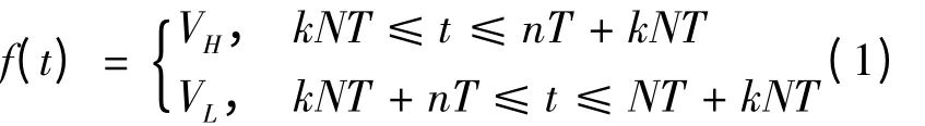
Where,T is the basic period of the counting pulse of microcomputer,that is,the microcomputer counts every T (the counter increases or decreases its value by 1),N is the number of counting pulse during one period of PWM wave,n is the number of high level counting pulse during one period of PWM wave,VHand VLare the voltage values of high and low levels of PWM wave,respectively,k stands for the k-th period,t is the time. Expanding the expression (1)into Fourier series,it can be gotten that:
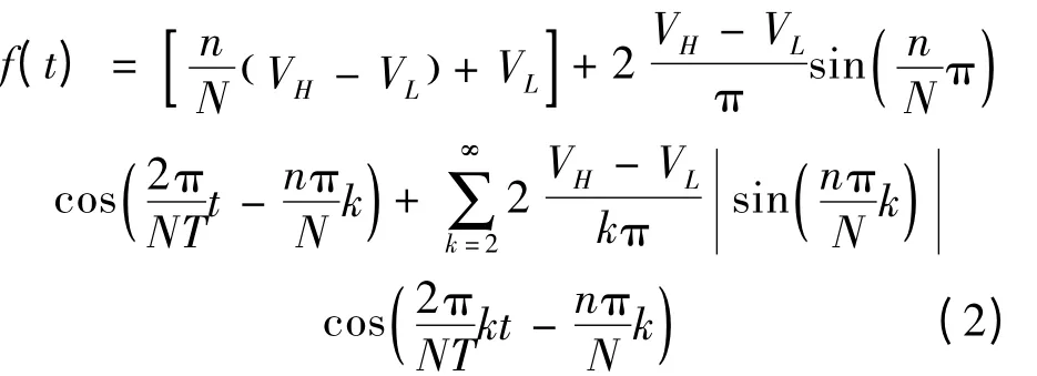
From the expression (2),it is known that the content included in the first brackets is DC component;the 2nd item is the first harmonic component;the 3rd item is the higher harmonic component whose degree is more than 1. The DC component in (2)has a linear relation to n,and as n increases from 0 to N,it changes between VL and VL+VH. This is exactly the output voltage that DAC needs. Therefore,if all harmonic components except DC component are filtered in (2),the transformation relationship between the PWM wave and the output voltage DAC can be obtained,that is,the PWM wave can be demodulated by a low-pass filter. In (2),the magnitude and phase of the 2nd item have something to do with n.The frequency of the 2nd item is 1/NT,and it is the basis for the design of low-pass filter. If the 1st harmonic component can be filtered well,the higher harmonic component should not nearly exist[6].
4. Design of circuit
Based on the demand for detected object,Fig. 2 shows the schematic diagram of A/D conversion using PWM.

Fig.2 Schematic diagram of A/D conversion using PWM
The principle of this circuit is to have weak signal detected by sensors amplified by differential amplification circuit. Then,after being precisely rectified,filtered and amplified,the waveform that accurately reflects original signal is obtained. Through comparing resulting wave and triangle wave,the PWM signal is generated,and is then amplified by the differential amplifier and outputted to processor.
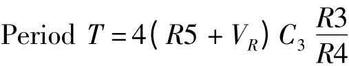
The triangle wave generator circuit is more important,so these circuits should be analyzed in detail. In order to analyze the circuits better as well as identify the key component,in this paper,when calculating the transfer function of each circuit,the zero-regulator resistor and the gain resistor will not be considered for the moment. Fig. 3 shows the schematic diagram of triangle wave generating circuit.The operational amplifier N1 forms the hysteresis comparator,and N2 forms the reverse integrator.They form positive feedback loop together and result in a self-excited oscillation. N1 outputs square wave.N2 outputs triangle wave. The hysteresis comparator has uplink hysteresis characteristics,and its reference voltage is 0 V. The square wave outputted by N1 is divided by potentiometer VR,and then becomes symmetric triangle wave through integrator.
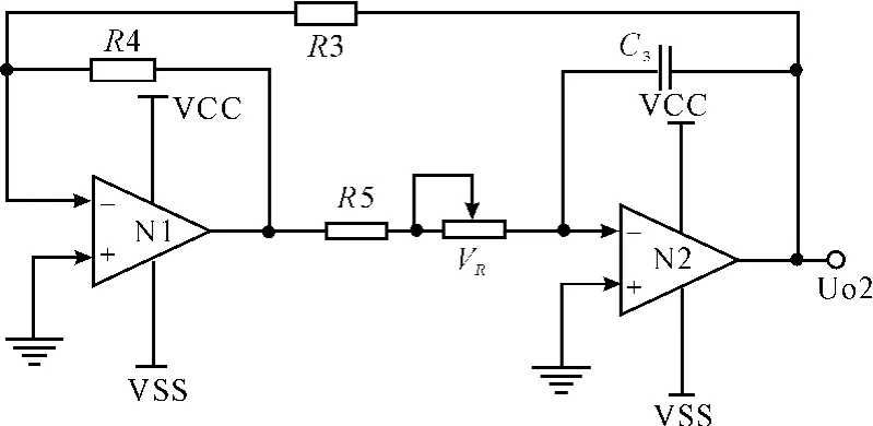
Fig.3 Triangle wave generating circuit
Maximum output voltage value

Umis usually 5 V.
By adjusting the value of VR,the output frequency of the triangle wave can be controlled,and which circumvents the interference frequency and makes PWM reach the required conversion precision.
5. The principle of processor processing PWM signal
During the A/D conversion,the PWM signal needs to be applied to the input port of other microcontrollers or processors. Take AVR microcontroller as the example. The PWM signal is applied to the two external trigger interrupt pins. One of them is set for rising edge triggered and the other is setup for falling edge trigger. Here as to priority,the rising edge interrupt response is posterior to the falling one.The program loop detection start is set for rising edge triggered. Once the rising edge interrupt responds,timer 1 is started,and begins timing TH1. When the falling edge interrupt responds,timer 2 is started up and begins timing TH2. At the time of the next rising edge interrupt,the values of TH1 and TH2 are read and then cleared. TH1 is one period;TH2 is the duration of low level. (TH1 ~TH2)/ TH2 is just the required pulse-width ratio. The flow chart of the microcontroller processing PWM signal is shown in Fig.4.
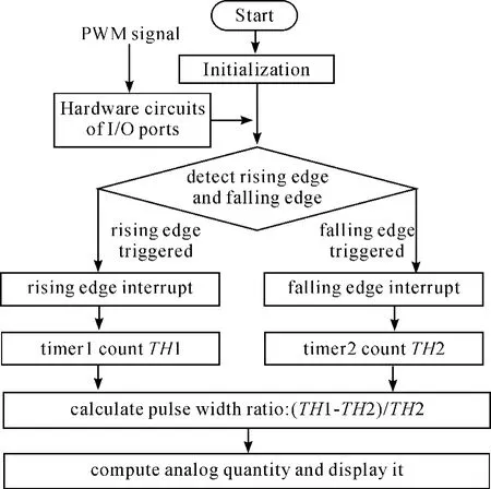
Fig.4 Principle of processor processing PWM signal
6. Signal processing and error analysis
When the signal is inputted into the circuit,a variety of factors may lead to the final output signal error. The most important factors include the zero drift of operational amplifier and error produced by code when the processor is processing the PWM signal.
6.1. Zero drift leads to error
Operational amplified can realize comparator.Because of the zero drift of operational amplifier,error will occur when the triangle wave and the input signal are compared. For example,if LM358 chip is used as comparator,the minimum distinguish voltage of the amplifier takes 100 μV,and the input signal voltage takes 5 V,after calculating it can be found that 0.02% error occurs in the output PWM signal.
6.2. Error produced by processor when processing PWM signal
The AVR microcontroller,which uses interrupt mode to count the time,is considered. When the interrupt occurs,the interrupt response time will result in the timing error. The interrupt response time mainly consists of three parts:the crystal frequency,the priority of interrupt in the program,and the processing speed of singlechip. The major error aspects introduced by the singlechip for the finally sample result are interrupt the response time and the timer timing.The higher the interrupt priority is,the faster the interrupt response time is,and thus the smaller the timing error is. Since the external trigger interrupt has the highest response priority,it is adopted;the higher the crystal frequency is,the faster the processing speed of microcontroller is,so the continuity of the output results is better. It can be seen in Fig.4 that both of the two interrupt responses will produce the delay to the start timing of the two timers. In order to reduce the error caused by this delay,after the rising edge interrupt opens the timer 1,and falling edge interrupt opens the timer 2,until the next rising edge interrupt occurs,the values of the two timers TH1 and TH2 are read and then cleared. During the process of result output,the error generated by the processor in operating the PWM signal is determined by the processor clock cycle and the triangular wave cycle. The conversion accuracy of the PWM A/D converter is the ratio of the triangular wave cycle and the microcontroller clock cycle. If the triangular-wave frequency (ie,the PWM signal frequency)is 4. 8 kHZ and microcontroller clock cycle is 50 ns,the conversion accuracy is 1/4 167. Use this circuit for A/D conversion can achieve 12-bit A/D conversion accuracy. Increase the cycle of triangular wave,the A/D conversion accuracy will decrease,and vice versa.
In addition,if the least square method is used to fit a large number of experimental data and compensate the output signal in the program,the error produced by various factors in the circuit can largely be eliminated. Thus the output results can approach the expected value as close as possible.
6.3. Analysis of experimental results
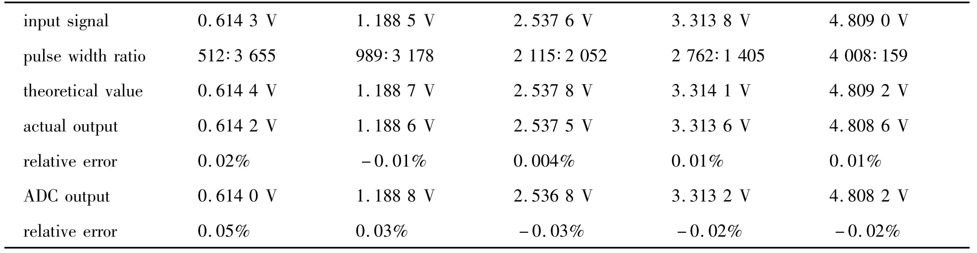
The conversion result of AVR microcontroller is compared with that of the 12-bit ADC. The frequency of PWM signal is 4.8 kHz. Processor clock cycle is 50 ns. The conversion accuracy using PWM is 1/4 167. Different analog signals are input and the PWM conversion circuit and the ADC are used to carry out the A/D conversion respectively. The resultant output analog signals as well as the relative error are listed in Tab. 1. The 2 ~5th lines in the table are all the conversion results gotten by using the PWM conversion circuit to implement A/D conversion,of which parts of the pulse width and the theoretical value are obtained by theoretical calculation;the relative error is obtained by dividing the difference between the actual output and input signals by input signal. The 6 ~7th lines list all the results using the ADC to complement A/D conversion. The relative error is gotten by dividing the difference between the ADC output and input signals by input signal.
The A/D conversion using AVR microcomputer is compared with 12 bits ADC. The frequency of PWM signal is 4.8 kHz. The clock cycle of processor is 50 ns. Using PWM to realize A/D conversion,the conversion precision is 1/4167. Different analog signals are input,and then are converted by using PWM conversion circuit and ADC respectively. The resulting analog signals and the relative error are shown in Tab. 1. The 2 ~5th rows of Tab.1 is the results using PWM conversion circuit and ADC. The parts of the pulse width ratios and the theoretical values are obtained by theoretically calculating. The relative error is obtained by dividing the difference between the actual output and input signals by input signal. The 6 ~7th rows are the results using ADC to realize A/D conversion,and its relative error is obtained by dividing the difference between the output of ADC and input signals by the input signal.
The experimental results in Table 1 are analyzed as follows. The A/D conversion error using PWM is lower than that using ADC. The maximum error of the two methods is both half of the resolution. According to the experimental results,using the PWM conversion circuit can achieve the same effect as using ADC.
The reliability experiment is made to the two A/D conversion modes. The transducer operate is put in low frequency state with larger interference. The result using PWM to implement A/D conversion has no change,but it has a greater error when using ADC to accomplish A/D conversion,which proves that the PWM conversion circuit for A/D conversion has a strong anti-interference ability.
What’s more,the use of the PWM conversion circuit for AD converter can easily adjust the resolution depending on the different input signal,and it will not affect the conversion rate,while the resolution of the AD converter is fixed to several values.Unlike the AD converter,the resolution and the conversion rate of PWM conversion circuit are not a pair of basic contradictions which has been proved in this experiment.
Tab.1 Compare these two means of A/D conversion
7. Conclusions
Through experimental tests of A/D conversion on flow,pressure and temperature control system,it can be seen that using PWM circuit for A/D conversion can outperform the effect of conventional A/D conversion chip in the aspects of anti-interference,conversion accuracy and circuit costs. In addition,as to PWM signal,the representation of the signal size is its pulse width rather than amplitude. The signal is always maintained in the form of digital signal (only the high and low forms of level),so it is not sensitive to the additive interference,which greatly improves the ability of anti-interference in the transmission which has been verified by this experiment. The ADC that adopts PWM circuit has received a novel utility patent,which is applied well in strong interference products,such as flow,pressure and temperature testing,as well as field detecting instruments.
The A/D converter which is based on the PWM principle has some other advantages:fast conversion speed,no need for a special A/D converter,and meeting a lot of high-speed cases;simple system,flexibility in adjusting resolution,lower power dissipation than the traditional AD conversion,and lower cost. This circuit can be applied to various cases which need transmit DC signal to AC and DC signals with strong anti-interference ability. If the rectifying modules are increased before filtering and amplifying the modules,this circuit can also be applied to the situations where AC signal with strong anti-interference ability need be transmitted.
[1] CHEN Zhijie.Noise shaping implementation in two-step/SAR ADC architectures based on delayed quantization error[Z]. Midwest Symposium on Circuits and Systems,2011.
[2] Wang Qiumei.The Research and Design of 16 bit Σ-△ADC Analog Part[D].Changchun :Changchun University of Science and Technology,2008.
[3] GANG Cundifu.Amplifier Design of OP[M].Ranslated by Wang Lin,Xu Yazhen,Li Wuping.
[4] CHEN Ping.The Design of A/D Converter Circuit Based on the Technology of PWM[J]. Control & Automation,2007,29:114.
[5] WANG Shuguang. The Design to Achieve Resolution of ADC[J].Machine Tool & Hydraulics,2007,35(7):201-202.
[6] WANG Lan,WU Haiqiang,Sun Zhuojun.Electronic Circuit Design Based on PWM filter for D/A[J]. Applied Science and Technology,2007,34(10):50-53.

- 机床与液压的其它文章
- Simulation and Optimization Analysis of Circuit Breaker Operating Mechanism
- Synchronous Motion Servo-control of Biaxial Cross Coupling Based on Intelligence Fusion Strategy
- Decoupling Control Algorithm of Online Self-tuning Based on DRNN
- Experimental Study on Mechanical Properties of Low Carbon Steel with Ultrasonic Vibration Tensile
- Wavelet Analysis Fault Information and Realization in Virtual Instrument
- Precision Measurement of Series Motor Housing Based on CMM