Two Quadrant DC/DC ZVS Quasi-Resonant Lou-Converter
WU Jianzhong, ZHANG Chuang,LIU Yingying
(1.Wuxi China Resoures Microelectronics Co. Ltd , Wuxi 214061, China;2. Wuxi Silicon Technology Co. Ltd, Wuxi 214028, China)
1 Introduction
In recent years the DC/DC conversion technique has been greatly developed. The main objective is to reach high power transfer efficiency, high power density and cheap topology in simple structure. However, even though high conversion efficiency has been achieved,switching converter designs possess several undesirable characteristics. Rapid switching of input or output currents can cause severe electromagnetic interference(EMI) problems, and the electromagnetic sensitivity(EMS) and electromagnetic compatibility (EMC) of the switching converter are also unreasonable.
If each switch in a converter changes its status when the voltage across it or the current through it is zero at the switching instant, the aforementioned shortcomings can be minimized. The technique employing the converter topologies and switching strategies, which result in zero-voltage or zero-current switching, is called soft-switching conversion technique. This softswitching conversion technique is used to minimize the aforementioned shortcomings. Since middle 1980’s, it has been very popular to use soft-switching technique for design of modern DC/DC converters[1~6].
Over last ten years, many Soft-Switching DC-DC converter were introduced in the open literature. The objectives of these topologies are to develop switching converters with high power density and efficiency.This was accomplished by additional components to the power stage to either limit the resonant period and/or utilize power device parasitic components.Unfortunately, most of the papers discuss the converters working under a single-quadrant operation only. Many industrial applications, however, desires the multiquadrant operation.
This project introduces a new Two-Quadrant DCDC Zero-Voltage-Switching(ZVS) Quasi-Resonant Luo-Converter (QI, QII). It proposes a new soft switching technique with a two-quadrant operation, which effectively reduces the power losses and largely increases the power transfer efficiency. This new converter also has the advantages of the high power density and simple structure with low cost.
2 Circuit Description
In this section, the concept of Zero-Voltage switching technique will be briefly introduced. It includes theoretical calculations and the circuitry of the two quadrants.
2.1 Zero-Voltage quasi-Resonant Buck Converter
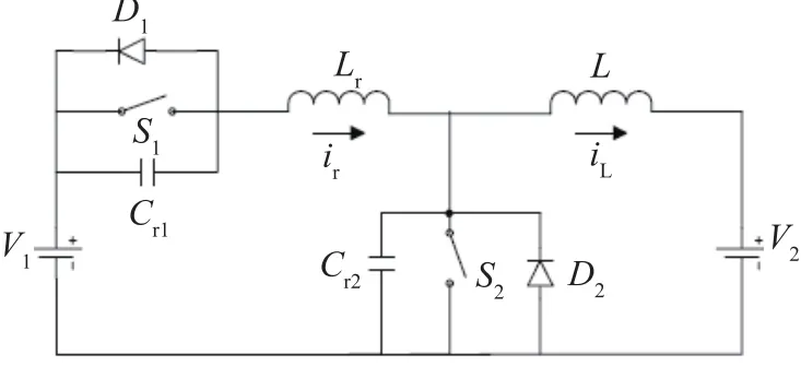
Fig.1 Two-quadrant DC/DC ZVS quasi-resonant luo-converter
Figure 1 shows the circuit configuration for a twoquadrant DC/DC converter. It combines the circuit configuration of each quadrant (Quadrant I and II). The circuit topology is simple as it consist only 2 electronic switches, 2 power diodes, 2 capacitors and 2 inductors.The operation for each quadrant can be fulfilled by applying a PWM control signal to either S1(for quadrant I) or S2(for quadrant II). There are two modes of the operation∶
Mode A (Quadrant I)∶ electrical energy is transferred from V1side to V2side;
Mode B (Quadrant II)∶ electrical energy is transferred from V2side to V1side.
In order to simplify the analysis of DC/DC ZVS QR Luo-Converter, the following assumptions have been made.
(1)The main inductor L is sufficiently large so that ILcan be treated as a constant current source[7].
(2)The power switches and diode are ideal, no forward voltage drops in the on-state, no leakage currents in the off-state, and no parasitics.
(3)The resonant capacitor Cris ideal.
2.2 Circuit Operation of Quadrant One
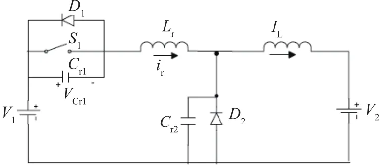
Fig.2 Equivalent circuit of quadrant one (Mode A)
Suppose, before S1is turn off, it carries the input current, Ii. Diode D2is off and no current is flowing into D2. At time t0, S1turns off, input current IIis diverted into capacitor Cr1. The following description summarized the circuit operation during each of the four stages.
(1)Capacitor Cr1Charging Stage [t0, t1]
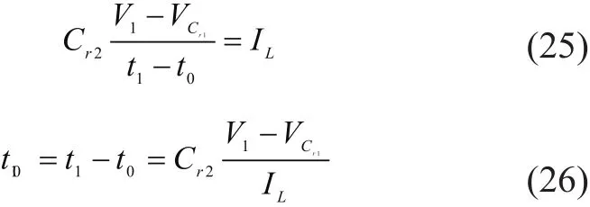
S1turns off at time t0= 0, current irflows through Cr1.The voltage across on Cr1, vCr1rises linearly.

At time t1, vCr1reaches V1-vCr2, diode D2conducts.The duration of this stage, t1-t0, can be determined from the following∶

(2)Resonant Stage [t1,t2]
D2turns on at t1, a portion of ILstarts to flow into D2.Initial condition∶

State equations∶
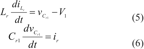
The state equations can be solved by

Where

In the half-wave mode of the operation, when VC1drops to zero at t2, it is clamped at the value by antiparallel diode, D1, which carries the reverse current.
At t2,

Where

The time interval t2-t1is that

(3) Inductor Current Rising Stage [t2, t3]
After t2, current irincreases linearly and reaches ILat time t3.
Initial condition∶

State equation∶

The duration of this stage, t32can be determined from

(4)Turning-on Stage [t3,t4]
At t3, D2turns off, irequals to IL, a portion of irstarts to flow into capacitor Cr2. Lrand Cr2form another resonant during interval [t3, t4].
Initial condition∶

State equations∶
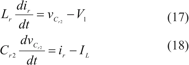
The state equations can be solved by

where the circuit characteristic impedance

Resonant frequency

The waveforms of vcrand irare shown in Figure3.
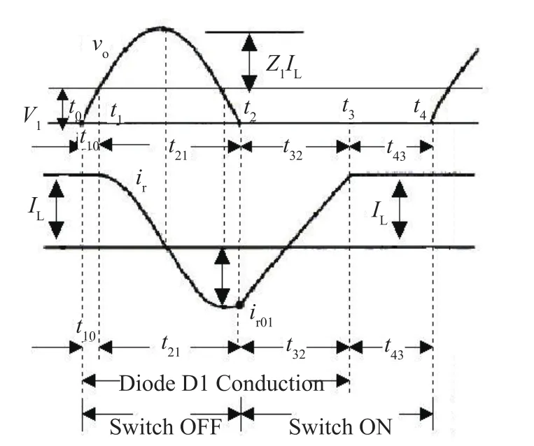
Fig.3 The waveforms of vcr and ir for quadrant one
2.3 Circuit Operation of Quadrant Two
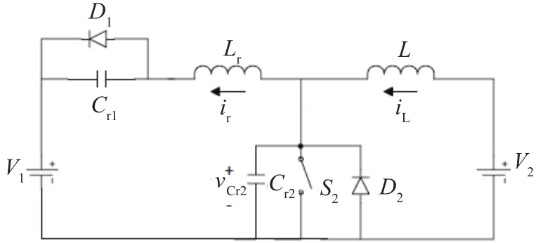
Fig.4 Equivalent circuit of quadrant two (Mode B)
Quadrant II also has four stages, The following description summarized the circuit operation during each of the four stages.
(1) Capacitor Charging Stage [t0, t1]
S2turns off at t0= 0, current flows into Cr2, the voltage on Cr2, vCr2rises linearly.
Initial condition∶

State equation∶

At time t1, vCr2reaches V1, diode D1conducts.
(2) Resonant Stage [t1,t2]
D1turns off at t1, a portion of ILstarts to flow into Lr.Initial condition∶

State equations∶
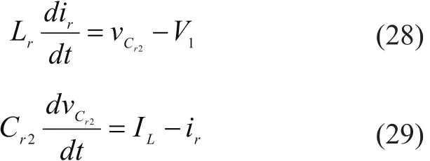
The state equations can be solved by

In the half-wave mode of operation, when vCr2drops to zero at t2, it is clamped at the value by the anti-parallel diode, D2, which carries the reverse current.
At t2,

Where

The time interval t2− t1is that

(3) Inductor Current Rising Stage [t2,t3]
After t2, current irdecreases linearly and reaches 0 at time t3.
Initial condition∶

State equations∶
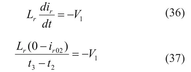
The time interval∶

(4)Turning-on Stage [t3,t4]
At t3, D1turns off, and a portion of ILstarts to flow into the capacitor Cr1. Cr1and Lrform another resonant during time interval [t3,t4].
Initial condition∶

State equations∶
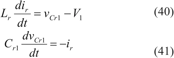
The state equation can be solved by

Duty Cycle∶

Time Period∶

Switching Frncy∶

The duration of this stage,t43, is an independent variable. By controlling the on interval t43of the switch,the average power supplied to the output stage can be controlled.
The waveforms that illustrate the simplified circuit operation are shown in Figure 5∶
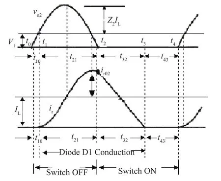
Fig.5 The signal waveforms of simplified quadrant II circuit
3 Design and Implementation
The actual implementation includes designing of electronic switches, control of output current and logic for switching between two quadrants.
3.1 PWM Single Generator, L-Resonator
The Luo-Resonator basically consists of three circuitry using operational amplifiers (OA). They are input comparator, integrator and output comparator.Figure 6 shows the circuit diagram of a Luo-resonator.
3.2 Switch and Control
As shown in Figure 7, R1provides an alternative path for the bootstrap capacitor because input, 36 V, is higher in potential than output, 12 V. Some of charging current always flow through R1 even if Return is at output potential.the bootstrap diode, capacitor CB and zener diode are external components strictly required for the operation in a standard PWM application. Local decoupling capacitors on the Vcc supply are useful in practice to compensate for the inductance of the supply line.
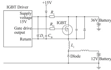
Fig.7 Switch and control
The circuit diagram for the switches and the driver is shown below as Figure 8.
The components used for the final circuit in Figure 8 are∶
IGBT - IRG4PSC71UD
IGBT Driver - IR2110
D3 - BYX15
R1 - 8.2 kΩ
RB - 10 Ω
CB - 10 μF/50 V
4 Data Acquisition and Analysis
The main objective of this project is to analysis the performance of the Two-Quadrant DC/DC converter.
There are two quadrant operations-QI and QII.Software simulation results in each operation are collected. The software simulation of the converter is carried out using MicroSim PSpice.
4.1 Software Simulation of Quadrant I
The Quadrant I of two-quadrant circuit is simulated using MicroSim PSpice simulation program. The simulation result is shown in Figure 9. It is clear that during time interval t3-t4there is a resonance formed by Cr2and Lr. How long the resonance can last dependent on the time interval t3-t4.
4.2 Software Simulation of Quadrant II
The simulation result is shown in Figure 10. It can beobserved that there is the resonance formed by Cr1and Lr.
5 Conclusion
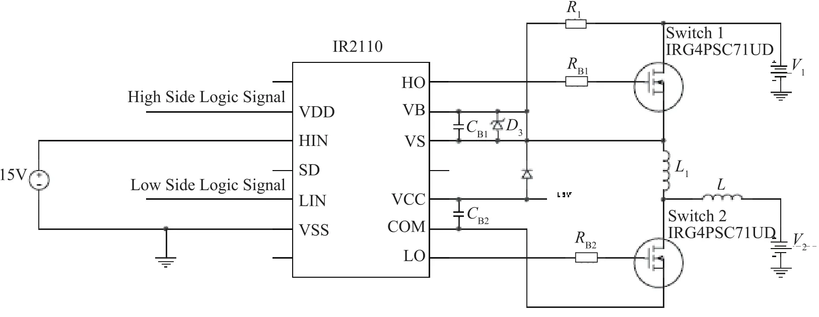
Fig.8 Final Schematic of the Circuit
In this project, a Two-Quadrant Zero-Voltage-Switching Quasi-Resonant Luo-Converter (QI & QII)was developed. The project is successful and fruitful. The software simulation has verified the theoretical analysis and calculations. With only two electronic switches,two power diodes, two capacitors and two inductors, the converter can perform as ZVS buck-converter (QI) and boost-converter (QII). This topology has made the Two-Quadrant converter simple and compact compared to the classical single converter. The overall performance of the converter has been improved by the introduction of Zero-Voltage-Switching technique.
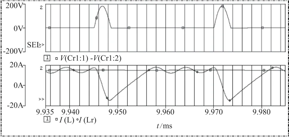
Fig.9 ir and vCr1 waveform of Quadrant I
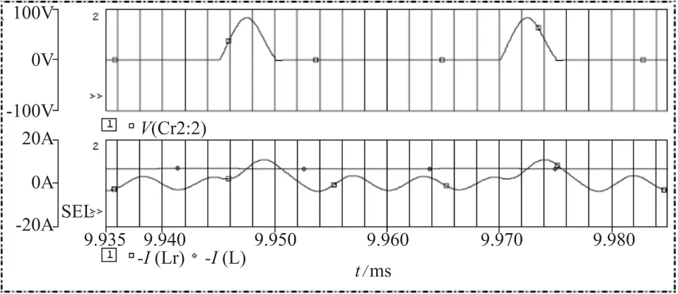
Fig.10 ir and vCr2 waveform of Quadrant II (f = 40 kHz,duty cycle = 80%)
Reference:
[1] C. J. Campbell, J. H. Laherrere. The end of the cheap oil[J]. Scientific America, March 1998.
[2] I. A. Khan. DC to DC converter for electric and hybrid vehicles[J]. Power Electronics in Transportation, 1994,113-122.
[3] G. Hua, C. Leu, F. C. Lee. Novel Zero-Voltage-Transition PWM Converters[J]. IEEE PESC Tec, 1992, 55-61.
[4] K. H. Liu, F. C. Lee. Zero-Voltage Switching Techniques in DC/DC Converter Circuits[M]. Power Electronics Specialist’s Conf. (PESE) Record, Vancouver, Canada,1986. 58-70.
[5] G. Hua, X. Yang, Y. Jiang, F. C. Lee. Novel Zero-Current Transition PWM Converter[J]. IEEE Power Electronics Specialist’s Conf. Rec., 1993. 538-544.
[6] A. K. S. Bhat. A Fixed-Frequency Modified Series-Resonant Converter∶ Analysis Design, and Experimental Results[J]. IEEE, Trans. On Power Electronics, 1995,10(6)∶766-775.
[7] Kassakian. Principles of Power Electronics[M]. Addison Wesley, 1995.

