Fabrication of Si3N4Nanopore and Detection of λ-DNA Molecules*
MA Jian ,LIU Lei,NI Zhonghua
(Jiangsu Key Laboratory for Design and Manufacture of Micro-Nano Biomedical Instruments,School of Mechanical Engineering,Southeast University,Nanjing 210096,China)
SNanopores are increasingly utilized as versatile sensors for detection and analysis of biological molecules[1-5].Such nanopore sensors are employed to analyze the ionic currents signals in which molecules passing through a nanopore will physically block the pore and produce spike like changes.The function has been focused on rapid sequencing of DNA using α-hemolysin and solid-state nanopores.All early work used α-hemolysin,a kind ofbiologicalnanopore which provides a ready made,atomically precise and repeatable pore structure.However,α-hemolysin have a range of limits,such as short lifetime and their sensitivity to extreme environmental conditions(e.g.,temperature,pH and salt concentration),which will likely be required to control DNA conformation.Furthermore,the small size of the α-hemolysin pore(diameter 1.3 nm)also limits biological molecules analysis to this order of size,for example,dsDNA cannot pass through α-hemolysin[3-4].Solidstate nanopores offer advantages over protein-based pores,such as size control,increased chemical,electrical,mechanical, thermal stability, and the potential of device integration[6].In this paper,a direct and simple method of preparation of nanopores will be introduced then the processed nanopores are used to investigate the translocation of λ-DNA molecules.
1 Fabrication of Si3N4Nanopores and Experimental Set up
The past 10 years have seen major development of solid-state single nanopores,aiming to address the limitations of biological pores[7-10].Several fabrication methods have been demonstrate,one of the most direct and simple method is to use FIB sputtering the thin membrane.
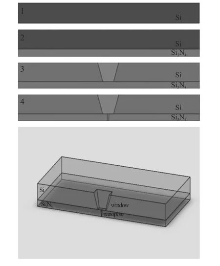
Fig.1 schematically illustrate the procedures of the processes of nanopore based on Si3N4membrane.The main concept of this method is a four-step process.First process is polishing the both side of Si wafer.The Si chip used is a 300 μm thick <100> n-type wafer and cut into 5 mm×5 mm.Second,the Si3N4layer on one side of the Si wafer are deposited using the LPCVD process.The thickness of the Si3N4membrane is about 100 nm.Third step is opening a window on the top of Si wafer using TMHA wet etching[11].At the bottom of the window,it form free standing Si3N4membrane.Fig.2 display the after etching structure for a 50 μm×50 μm window.Finally,the sample was placed in a focused ion beam(FEI STRATA FIB 201)operated at 300 kV.The use of a tightly focused ion beam sputter material of the Si3N4membrane and hence create a nanopore.

Fig.1 Schematic Illustration of the Fabrication Processes(Right)and the Cross-Section View of Our Device(Left)

Fig.2 Optical Image of the Structure for a 50 μm×50 μm Window Coated with PDMS
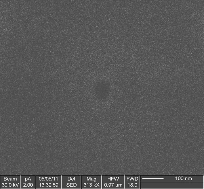
Fig.3 is the ion-beam image of nanopores sculpted in Si3N4membrane immediately after its formation by the intense ion beam.There are two main factors affect the diameter of the nanopore:the energy of the ion beam and the time of sputtering.In order to accurately detect the DNA sequence,the diameter of the nanopore must within 5 nm.The nanopore can shrink gradually to a single-nanometre when it is exposed to a low energy ion beam or a high energy electron beam[8,12-15].Material deposition is another way to reduce the size of the nanopore[16].This will be done in our future work.

Fig.3 Ion-Beam Image of Nanopores Sculpted in Si3N4Membrane by Focused Ion Beam.The diameter is about 60 nm.
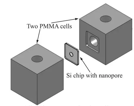
Two PolymethylMethacrylate(PMMA)cells were designed to mount the silicon support chip between two liquid reservoirs filled with buffered electrolytic solution.Fig.4 shows a schematic of the cell assembly.The Si chip was embedded in the groove of one cell,and the two part was linked together with PDMS.The nanopore formed the only connection between the two compartments.Solutions could be exchanged easily within each compartment by flowing liquid through the channels.Ag/AgCl electrodes immersed in the hole of the chamber are connected to a patch clamp amplifier(EPC 10USB,HEKA Instruments,Germany)to measure changes in ionic current with picoamp sensitivity.The device is placed in a double faraday cage enclosure to reduce electrical noise.

Fig.4 Exploded View of the Cell Assembly
Salt solutions were prepared by adding 18 MΩcm deionized water to 99.99%purity potassium chloride.48.5 Kbp double-stranded λ-DNA(TIANDZ,Beijing)was used in the translocation studies.
2 Result and Discussion
The value of the nanopore conductance at five different potassium chloride concentrations was obtained by sweeping the voltage over a range of±1 V at a scan rate of approximately 200 mV as Fig.5 shows.Fits to the data yield the value of the pore conductance.Its value clearly decreases as the potassium chloride concentration is lowered.In all experiments,the I- V curves show rectification,a characteristic property of small nanopore with charged surfaces,and asymmetric geometries or charge distributions[1].

Fig.5 Current voltage characteristics for a single 54-nm-diameter pore at KCl concentrations of 0.001 mol/L,0.01 mol/L,0.1 mol/L,1 mol/L,and pure H2O.The pore shows a concentration dependent rectification of the ionic current due to its negatively charged inner surfaces and tapered morphology of pore’s internal structure.
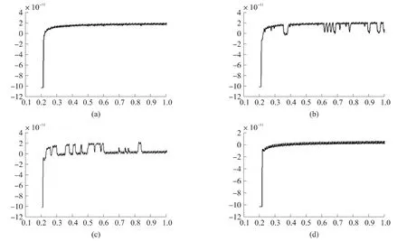
For DNA translocation,a constant voltage of 1 V was applied.When DNA was added into the negative electrode side,spike-like changes were investigated in the current like Fig.6 shows.This current signal was digitized at 200 kHz and low-pass filtered with a cut off frequency of 10 kHz.In order to increase the signal-tonoise ratio,the data was subjected to an additional external filter of 100 Hz.For the same purpose,we even coated silicon chip with PDMS as Fig.3 shows[17].

Fig.6 (a)There is just 0.5 mol/L KCl solution without DNA molecules in the chamber applied with 1 V,the basic current is about 20 pA and there is no block signal;(b)Added 48 Kbp double-stranded λ-DNA(128 ng/mL)in the cis-chamber,spike-like changes are observed.From the trace,we can see the block current is down to zero from the basic current;(c)The block phenomenon become more and more serious as time goes by;(d)Finally,the basic current is completely dropped to zero.
For this phenomenon,we believe that before the DNA molecules added into the chamber,there are just K+(red particle)and Cl-(blue particle)ions in the solution as Fig.7(a)shows.A voltage is applied,the movement of ions form the basic current.When DNA added into the negative side,they will swim to positive electrode for their negative charge.They will cause a decline in the basic current as they pass the nanopore,because their size is much larger than the ions.In our experiment we found the obstruction become more and more serious over time.And the nanopore will be blocked completely like Fig.7(c).Then we applied a reverse electric field,the blocked nanopore will be through again.It seems to reverse the direction of DNA’s movement.

Fig.7 The Process of DNA’s Translocation
3 Conclusion
In this paper,a direct and simple method to fabricate nanopores based on Si3N4membrane is presented.Two PMMA cells were designed to mount the silicon support chip between two liquid reservoirs.When we add λ-DNA molecules into the negative chamber,spike-like changes were observed in the current.Nanopore-based DNA sequencing is a new single-molecule technique.There are still a lot of challenges although it has made some progress.First of all,it is very difficult to fabricate a nanopore within 5nm.Second,the speed of DNA translocation is too fast to capture the information,so we need improve our measurement speed to 1Mhz at least.Finally,the noise is another thorny problem[18-20].
[1]Healy K,Schiedt B,Morrison A P.Solid-State Nanopore Technologies for Nanopore-Based DNA Analysis[J].Nanomedicine-Uk 2,2007(6):875-897.
[2]Branton D,Deamer D W,Marziali A,et al.The Potential and Challenges of Nanopore Sequencing[J].Nat Biotechnol,2008,26(10):1146-1153.
[3]Song L,Hobaugh M R,Shustak C,et al.Structure of Staphylococcal a-Hemolysin,a Heptameric Transmembrane Pore[J].Science,1996,274:1859-1866.
[4]Long Ma,Scott L.Cockroft:Biological Nanopores for Single-Molecule Biophysics[J].ChemBioChem,2010,11:25-34.
[5]Healy K.Nanopore-Based Single-Molecule DNA Analysis[J].Nanomedicine,2007(2):459-481.
[6]Skinner G M,Michiel van den Hout,Broekmans O,et al.Distinguishing Nucleic Acids Using Solid-State Nanopores[J].Nano Lett,2009,9(8):2953-2960.
[7]Dekker C.Solid-State Nanopores[J].Nature Nanotech,2007(2):209-215.
[8]Storm A J,Chen J H,Ling X S,et al.Fabrication of Solid-State Nanopores with Single-Nanometre Precision[J].Nature Materials,2003(2):537-540.
[9]Li Jiali,Stein D,McMullan C,et al.Ion-Beam Sculpting at Nanometre Length Scales[J].Nature,2011,412(6843):166.
[10]Sha Jingjie,Ni Zhonghua,Yunfei Chen,et al.A Novel Method of Fabricating a Nanopore Based on a Glass Tube for Single-Molecule Detection[J].Nanotechnology,2011,22:175304.
[11]Yu Xiezheng,Ye Yinghua,Shen Ruiqi.Investigation of TMAH for Fabricating Micro Nozzle Array[J].Chinese Journal of Sensors and Actuators,2012(2):1004-1699.
[12]Min Jun Kim,Meni Wanunu,David C,et al.Rapid Fabrication of Uniformly Sized Nanopores and Nanopore Arrays for Parallel DNA Analysis[J].Adv Mater,2006,18(23):3149-3153.
[13]Min Jun Kim,Ben McNally,KazuyoshiMurata,etal.Characteristics of Solid-State Nanometre Pores Fabricated Using a Transmission Electron Microscope[J].Nanotechnology,2007,18:205302.
[14]Bola George H,Tang Yuye,Chen Xi,et al.Nanopore Fabrication in Amorphous Si:Viscous Flow Model and Comparison to Experiment[J].Journal of applied physics,2010,108:14310.
[15]Shi Mingfu,Jiao jiwei,Bao xiaoqing,et al.Novel Fabrication Technique for Nanogroove Using Ion Beam Etching[J].Chinese Journal of Sensors and Actuators,2006(5):1462-1465.
[16]Peng Chen,Toshiyuki Mitsui,Damon B Farmer,et al.Atomic Layer Deposition to Fine-Tune the Surface Properties and Diameters of Fabricated Nanopores[J].Nano Lett,2004,4(7):1333-1337.
[17]Tabard-Cossa V,Trivedi D,Wiggin M,et al.Noise Analysis and Reduction in Solid-State Nanopores[J].Nanotechnology,2007,18(30):-.
[18]Golovchenko J A,Garaj S,Hubbard W,et al.Graphene as a Sub-Nanometer Trans-Electrode Membrane[J].Nature,2010,467(7312):190.
[19]Dekker C,SchneiderG F,Kowalczyk SW,etal.DNA Translocation Through Graphene Nanopores[J].Nano Lett,2010,10(8):3163.
[20]Drndic M,Merchant C A,Healy K,et al.DNA Translocation Through Graphene Nanopores[J].Nano Lett,2010,10(8):2915.

