有关MEMS结构运动过程中产生和辐射电磁波的研究*
张晓艳,黄庆安,韩 磊
(东南大学MEMS教育部重点实验室,南京210096)
Microelectromechanical Systems(MEMS)technology is acquiring an increasing number of applications because of its proven better performance compared to currently available state of art solid state devices[1].One of the unique features of MEMS is that it involves movement of micro mechanical structure that gives rise to new ways of sensing and actuating.Although there already have been many successful applications,it is believed that there is still much space left to be discovered in the application of structural movement in MEMS[2].
One such potentiality lies in the electromagnetic(E-M)domain.It is well known that moving charges may produce E-M field and wave[3-5].Movement of MEMS structures is a very effective source of moving charges.At least two principles are possible to produce E-M wave by MEMS.First,movement between two MEMS electrostatic structures,like in parallel capacitance,or comb interdigited capacitance,directly alters the electric field in space and generates E-M wave.Second,movement of MEMS structure carrying net charges also produces E-M wave.These origination and transmitting of E-M wave by moving structures may occur in every type of MEMS device and provide plenty of possibilities of both applications and interferences.
Unfortunately,although there were numerous literatures on designing radio-frequency(RF)and microwave MEMS device[6-7],the dynamic coupling mechanism between MEMS structural movement and E-M wave in space is rarely reported.Previous effort mainly considered E-M characteristics of a static or quasi-static MEMS structure[8-10],instead of the dynamics.This paper presents an early study on the coupling physics between mechanical,electrical and E-M energy domain of typical MEMS structure in dynamic movement.Models in each energy domain are established in turn to find out what kind of E-M wave a moving structure can generate.Parametric study is performed to understand what may influence the E-M wave.Numerical simulations are used for validation.
1 Coupled Fields Modeling
1.1 Representative model and simplification
Since there are so many different shapes of moving structure and types of movement in MEMS,a thorough investigation is not practical at this stage.A most representative model is established instead.As shown in Fig.1,the model consists of a wave guide structure with a gap in the center.The gap is formed by the upper area and bottom area of the wave guide structure.The upper area is movable and the bottom area is fixed.So it is reasonable to think of the gap as a conventional parallel capacitance with movable upper plate and fixed bottom plate.In real cases,the waveguide may be coaxial cable,micro strip,coplanar waveguide(CPW)and so on,and the gap corresponds to structures like switch,phase shifter and reconfigurable capacitance and so on.
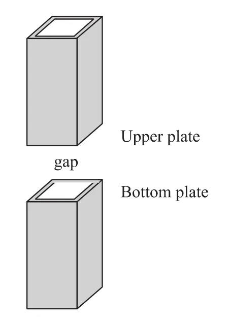
Fig.1 Representative model of MEMS structure that can produce E-M wave
The key point of the model is that most of E-M wave transmitted or radiated into the open space is screened by the ground of the wave guide except the gap region,so that the movable gap becomes the only efficient source of the E-M wave.Any other topology structure of MEMS can be regarded as a superposition of this model and those of other common structures.As for this model,it can further be regarded as a“quasi”basic element antenna subtracted from a full waveguide,as shown in Fig.2.The element antenna is“quasi”because here it cannot be considered as a line with no diameter.Actually there is a diameter value equal to the length of the plates.The focus of our study is on the quasi element antenna model where the length of the element(i.e.the height of the gap)varies with the movement of MEMS structure.It is obvious that the element antenna is just the“reciprocal”model of the gap,so they are so much distinguished in the following analysis.
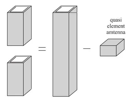
Fig.2 Simplification of the representative model in Fig.1
1.2 Origin of E-M wave
Using dynamic mechanical analysis of any MEMS structure,it is always possible to obtain an analytical expression ofmovementofthe upperplate ofthe gap,u(t).So the variation of the gap height g(t)is given by

The movement of the upper end towards the bottom plate has two results in the electric domain.Both may give rise to E-M wave.
First,as the gap height changes,the capacitance of the gap changes,and charges flows in and out to become electric current that may generate E-M wave.This can well be considered as the charging or discharging problem of the gap capacitance in Fig.1.The charging speed is affected by two factors.The first one is the charging time constant of the system.The other one is the variation period of the capacitance,like the time length required for the gap to move from the maximum height to the minimum one and then back again to the maximum.Usually,with agood conductorin the waveguide and a very small gap capacitance,the time constant of electrical charging(around 10-9s)is much smaller than the mechanical variation period(around 10-5s).So it is reasonable that the charging is only related to the variation of the gap capacitance and the charging time can be neglected.Assume the gap voltage V is a constant,the dynamic charges Q(t)on either plate of the gap can be denoted by

where C(t)is the dynamic capacitance of the gap.Based on the result in section 2.1,it is approximately given by

where S is the area of the gap plates.
Second,the net charges on the upper plate moves,and the movement may generate E-M wave directly.The bottom plate is also charged,but it does not move.The other part of the waveguide conductor is electrically neutral although there are moving charges and currents in them.So the upper plate is the only source of net charges movement,and it produce E-M wave in a unique and different way from the first one.The amount of the moving charges is still Q(t)as above,and the acceleration of their movement a is given by

The last important point is,according to the theory of antenna,most part of the E-M wave generated between the two plates is constrained within the central area and cannot be radiated into the open space.Only the fringe part of the gap is able to generate E-M wave we concern in this paper.As in Fig.3,the electric lines in the switch model diverge into the open space only around the corner of the plate.Thus the effective charges Qe(t)as the source of E-M wave on the corner of the gap is

where η denotes the ratio of the charges on the corner to those on the whole plate[11].
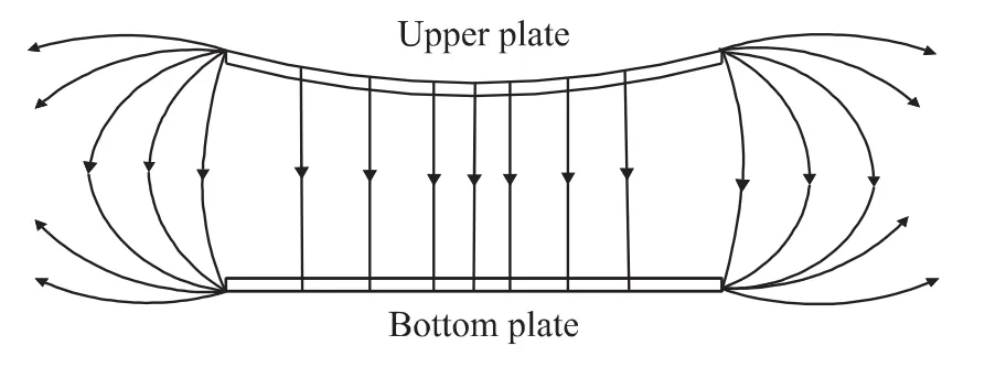
Fig.3 Charges on the corners of the gap capacitance are the effective origin of E-M wave
For both origins mention above,their effective charges are the same,namely the corner charges Qe.Hence the effective currents that generates open space E-M wave is denoted by

As a general case,the gap height changes periodically at an angular frequency of ω,so both charges and current will alter periodically,and the current can be denoted by

where Ieis the magnitude of the altering current.
1.3 E-M wave generation and radiation
For the first origin,the electric current through gap capacitance charging during movement,its generation of E-M wave can well be modeled as that of an element antenna carrying altering current,as shown in Fig.2.As mentioned before,the antenna model is just the reciprocal model of the gap.It generates an EM wave as[7]
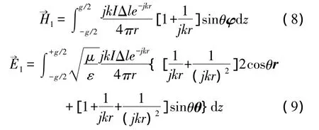
where μ and ε are the magnetic permeability and dielectric constant of the space,k is the magnitude of the E-M wave vector,r is the distance from the center point of the antenna,θ is the angle away from the length direction of the antenna,vector r,θ and φ are the unit vector in the radical,axial and tangential direction of the spherical coordinate system.The center point of the antenna is the origin of the coordinate system.
For the second origin,the net charge movement on the upper plate of the gap,the generated E-M wave is given by[5]
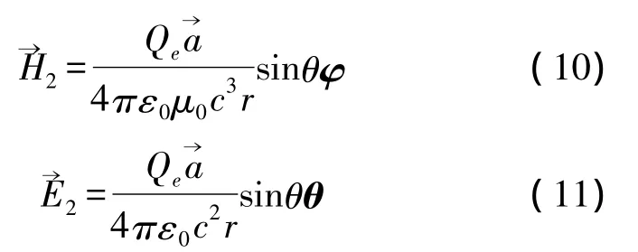
Where a is the acceleration of the charges.The final EM wave is the superposition of both.
2 Case study and discussion
Case study is performed to investigate the real EM wave generated by moving MEMS.A typical capacitance type switch structure is used as the realistic model of the movable gap.The geometric model of the switch is shown in Fig.4.The material and geometrical parameters of the switch is listed in Table 1.The theory of capacitive type switch is the rather mature and not the focus of our study.The known formulas in related textbook[12]are referenced for the electro-mechanical analysis of the switch.The movement of the switch gap is obtained and substituted into Eq.1 and Eq.4 for the consequent calculation.
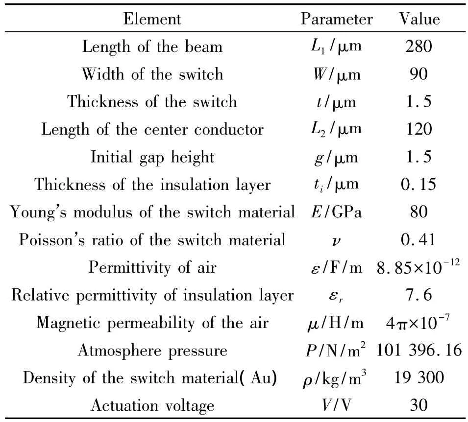
Table 1 Material and geometrical parameters
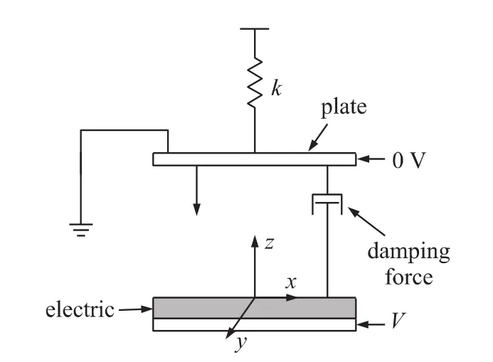
Fig.4 Geometric model of the capacitive type switch
To validate the analytical model,finite element(FE)analysis by the HFSS software is performed.HFSS is unable to perform a real dynamic coupling field analysis of the mechanically movable gap.It is also hard to perform a parametric study in its graphics interface.So it is only used to validate the antenna model.Fig.5(a)shows the vector diagram of the generated electric field around the element antenna in space simulated by HFSS.The size of the simulation volume is 20 mm×20 mm ×20 mm.Fig.5(b)shows the analytical result from section 2 of the electric field intensity component Erat θ=0°,which is located at the red region of Fig.5(a).The values match in orders of magnitude at the boundary and thus validate part of the analytical model.

Fig.5 Simulated electric field intensity of the antenna model from(a)HFSS results,(b)analytical results.They match in order of magnitude at the boundary region
Next,the parametric study is performed to see what factors may influence the electric field intensity and to what extent their influences may be.The first factor is the distance away from gap.Fig.6 shows the intensity of Eθat θ=90°and Erat θ=0°with respect to radius r when the line frequency f=100 kHz.These two components are selected for investigation because when the gap is mounted in plane or out of plane on a MEMS chip,respectively,the maximum values of the generated E-M wave must come from the Ercomponent at θ=0°and the Eθcomponent at θ=90°,respectively.It is seen that both components move very slowly within the microscale range.For a normal size of a MEMS chip,like 1 cm,the magnitude of the radius r with altering frequency of the gap at f=100 kHz generated electric field at the other side the chip is nearly the same as that nearby the origin gap.This may mean a universal influence of the generated E-M wave to all the devices on the same chip.

Fig.6 Erat θ=0°and Eθat θ=90°with respect to
The second factor is the altering frequency of the gap height.It is the most important factor that may enhance the effect of the generated E-M wave.When the frequency increases,the variation period of the gap height is shortened,and the current through the element antenna and the generated E-M field are increased.Fig.7 shows the electric field components at r=1 cm with respect to the altering line frequency f.It is seen that with the increase of the frequency,the intensity of the generated electric field can be increased 0.15 V/m,which is large enough to induce E-M interference in the whole 1 cm×1 cm chip area.Although it is not possible for current MEMS switch to vibrate or actuate at such a frequency,the next generation of submicron and nano structure are very likely to encounter such a problem.

Fig.7 Erat θ=0°and Eθat θ=90°with respect to altering line frequency f of the gap at r=1 cm
The third factor is the gap height itself.It affects both the length of the element antenna and the altering charges.Fig.8 shows the result at f=100 kHz and r=1 cm.The generated E-M field intensity increases with the gap height significantly.Although increasing the gap height may improve the isolation characteristics of most switches,the generated E-M wave and thus the E-M interference to the other MEMS device may be increased.It is observed that the intensity of the electric field is increased linearlywith thegap heightand theErcomponent at θ=0°is increased 5 times when the gap height changes from 1 μm to 5 μm.From the analysis above,the E-M field is influenced by the distance away from the gap most.
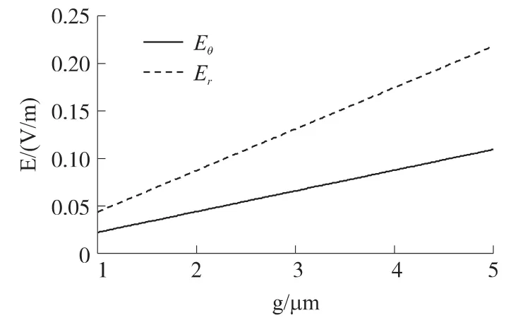
Fig.8 Erat θ=0°and Eθat θ=90°with respect to gap height g with f=100 kHz and r=1 cm
At last,the E-M wave generated by the two origins is compared in Fig.9.It is seen that the intensity of the E field generated by the two origins differ greatly.It is because the velocity of the charges which move with the plates are relative small.Although E2can be ignored compared with E1,this problem may show up in the future high speed MEMS devices.

Fig.9 Comparison of the generated E-M waves of the two origins in section 2.2

Fig.10 Approximate distribution of the generated E-M wave on a real chip with another switch located 1cm away from the movable gap.The gap is mounted(a)out of plane and(b)in plane,both at the edge of the chip.
For simplicity and clarity,the analysis above assumes an infinitely large space as the boundary condition of the E-M wave.The real boundary conditions are much more complex.Fig.10 shows two examples where the movable gap is mounted in plane and out of plane on a chip that contains another switch at a distance of 1cm from the gap.HFSS is used to simulate an approximate distribution of the generated E-M wave on the whole chip.Comparing the results with those obtained before at infinitely large space,it is found that the E field on the real boundary is much bigger than the free space.In the real boundary conditions,the E-M wave is scattered on the interface and induces variable charges which is the secondary source radiating E-M wave.The MEMS switch in the picture has complex boundary conditions.The EM wave is reflected and refracted several times on the interface.As a result,the intensity of E-M wave will increase.And the E-M wave concentrates in the gap of the switch.It is because this semi-enclosed structure is more declined to constraint E-M wave respect to the open structure.
3 Conclusion
Through a couple field analysis of a movable gap in a waveguide,it is proved that the movement of the gap is able to generate considerable E-M wave into the open space at a proper condition.The E-M wave comes from both the electric current charging the dynamic variable gap capacitance and the net charges in movement.Parametric study shows that the generated E-M wave may propagate in centimeters without considerable loss in the open space.The frequency of the gap has the biggest influence on the magnitude of generated E-M wave.It also increases with the height of the gap.Structures on chip may hinder or absorb part of the generated E-M wave,but the complex boundary conditions also result the gather of the E-M wave in the structure.And it may be influence the operation or the reliability of the device.The work indicate that dynamic coupling of the mechanical movement and E-M wave,which is often neglected in previous design,has to be taken into consideration with the continuousminiaturization ofthe MEMS structure and higher operation frequency.
[1]郭兴龙,蔡描,刘蕾.Ku波段硅基MEMS可重构微型天线设计[J].传感技术学报,2006,19(6):2425-2427.
[2]袁晓林,黄庆安,廖小平.电容式RF MEMS开关开关过程产生的电磁波模型和分析[J].传感技术学报,2006,19(5):1945-1950.
[3]Sammie Giles,Jr.(Ret.).Poynting Vector of a Uniformly Moving Point Charge[C]//41st Southeastern Symposium on System Theory,2009.169-170.
[4]Vernon Cooray,Gerald Cooray.The Electromagnetic Fields of an Acceletating Charge:Application in Lightning Return-Stroke Models[J].IEEE Transactions on Electromagnetic Compatibility,2010,52(4):944-955.
[5]Pannofsky W K H,Phillips M.Classical Electricity and Magnetism[M].Reading,MA:Addison-Wesley,1962.
[6]ReenaAl-Dahleh,RaafatR Mansour.High-Capacitance-Ratio Warped-Beam Capacitive MEMS Switch Designs[J].Journal of Microelectromechanical Systems,2010,19(3):538-547.
[7]Oren Aharon,LiorGal,YaelNemirovsky.HybridRF-MEMS Switches Realized in SOI Wafers by Bulk Micromachining[J].Journal of Microelectromechanical Systems,2010,19(5):1162-1174.
[8]Wong C H,Tan M J,Liew K M,et al.Electrical Characterization of RF Capacitive Microswitch[J].Sensors and actuators A,2003,102(3):296-310.
[9]Vitaly Leus,David Elata.On the Dynamic Response of Electrostatic MEMS Switches[J].Journal of Microelectromechanical Systems,2008,17(1):236-243.
[10]Sudipto K De,Aluru N R.Full Lagrangian Schemes for Dynamic A-nalysis of Electrostatic MEMS[J].Journal of Microelectromechanical Systems,2004,13(5):737-758.
[11]Hanno Hammer.Analytical Model for Comb-Capacitance Fringe Fields[J].Journal of Microelectromechanical Systems,2010,19(1):175-182.
[12]Rebeiz G M.RF MEMS Theory,Design,and Technology,chapter,3,John Willey& Sons(2003).

