Z形石墨带的电子输运性质:形状与尺寸效应
徐 宁 孔凡杰 王延宗
(1盐城工学院物理系,江苏盐城224051; 2淮阴工学院物理系,江苏淮阴223003)
1 Introduction
Due to amazing electrical properties,the graphene nanoribbons(GNRs)have attracted much attention in recent years, which can be prepared either by cutting,1mechanically exfoliated graphenes,2or by patterning epitaxially grown graphenes.3,4Based on the simple tight-binding model or Dirac′s equation, the electronic structure5,6and transport properties7,8of GNRs were explored.It is shown that GNRs with zigzag shaped edge (ZGNRs)are metallic,and that GNRs with armchair shaped edge(AGNRs)can be either metallic or semiconducting de-pending on their widths.These pioneering works elucidated that the integrated nanoelectronic circuits can be realized only by continuous graphene.
Recently,some groups have already demonstrated that the graphene can be cut in many different shapes and sizes,opening the door to the fabrication of graphene-based nanodevices such as graphene quantum dots,9-11field effect transistor,12,13quantum rings,11,14,15and antidot arrays.16More recently,the integrated graphene circuits have been proposed with a variety of L-shaped junctions.17It is shown that the L-shaped GNR with 120°turn(included angle θ=60°)is nearly reflectionless,similar to that of straight strip,while the L-shaped GNR with 60° turn(included angle θ=120°)has high reflectance to the electrons.The single junction is found in the integrated graphene circuits,but there also exist many L-shaped junctions.Electron scattering between junctions will play an important role in determining the electric conductivity of circuit.Thus the electron scattering between the junctions upon the conductance of circuit deserves our exploration.
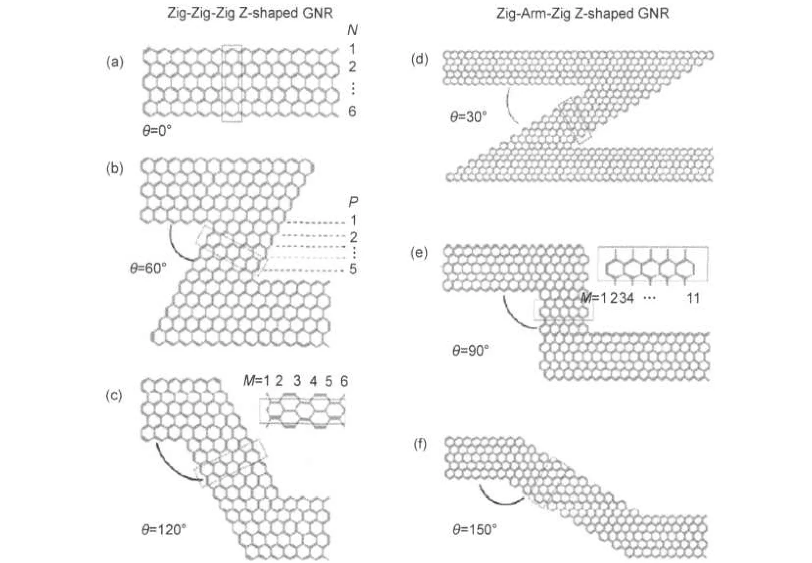
In this work,we focus mainly on the shape and size effects upon the conductance of the Z-shaped graphene nanoribbons (Z-shaped GNRs).For simplicity,we consider only the two simplest types Z-shaped GNRs.The first type of Z-shaped GNRs is Zig-Zig-Zig Z-shaped GNRs,in which the GNR between two corners and the semi-infinite leads consists of ZGNRs.The second type of Z-shaped GNRs is Zig-Arm-Zig Z-shaped GNRs,in which the GNR between two corners consists of AGNRs.The numerical results show that the Z-shaped GNRs have potential application in designing functional nanocircuits.
2 Theoretical methods and models
To explore the electronic properties of the Z-shaped GNR junction,we divide the Z-shaped GNR into three regions(as shown in Fig.1):the left lead,the Z-shaped junction region,and the right lead.The width of the leads and the width of GNR between the two corners are labeled by N and M,respectively.The length between the two corners is labeled by P.θ is the included angle of junctions.The Z-shaped GNR is described by a tightbindingmodelwithoneπelectronperatom,17,18

where εiis the site energy and VPPπis the hopping matrix element between the nearest neighbors.{ci*,cj}are the creation and annihilation operators at site i and j.In the absence of external field,the on-site energy εiis set to be Fermi energy EFand VPPπ=-3 eV.The density of states(DOS)and transmission coefficient of Z-shaped GNR are obtained within the Green′s function formalism.Thus,DOS of the Z-shaped GNR is calculated by19,20

Gr=is the retarded Green′s function,where HCis the Hamilton of the middle junction.andrepresent the self-energy of left and right leads,which can be calculated by iterative procedure.The transmission coefficient between the left and right leads can be calculated in terms of the system Green′function as21-25

Fig.1 Schematic view of Z-shaped GNRsθ:included angle.Each Z-shaped GNR consists of two semi-infinite leads and the Z-shaped junction region.The rectangle represents a unit cell in scattering region.

3 Results and discussion
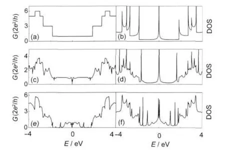
The conductance and the corresponding DOS of the Zig-Zig-Zig Z-shaped GNRs with N=6,M=6,P=5 are shown in Fig.2.For comparison,the conductance of the perfect ZGNR with N=6 is also shown in Fig.2(a).It can be seen from Fig.2 (a)that the ZGNR with N=6 exhibits the perfect steplike features with one unit of quantum conductance at about EFdue to one open channel,consistent with the previous results7,8.The corresponding DOS is shown in Fig.2(b).From Fig.2(b),a prominent DOS peak is observed at EF,because the corresponding electrons are completely localized on the edge sites of ZGNR.8For θ=60°,a small conductance gap is found at EF,a metal-semiconductor transition existing there.The origin of conductance gap is due to low velocity electrons at the EFand can be understood as follows.In a perfect ZGNR,the velocity (dE/dk)of electrons is nearly zero,where E and k represent the energy and wave vector,respectively.The low-velocity incident electrons at EFare reflected by the junctions.As shown in Fig.3(a),the electrons are localized on the lead edges,and no electrons can transmit the Z-shaped junction region at about EF. In addition,the overall conductance is depressed with varying resonance peaks.The conductance fluctuation arises mainly from the local resonance of bound states and/or quasibound states.Specially,one unit of quantum conductance is observed in low-energy region,which illustrates that the low-energy incident electrons around EFcan easily transmit through the Z-shaped junctions.In Fig.3(b),the spatial distribution of local density of states(LDOS)shows that the low-energy incident electrons in low-energy region are extended states between the two corners.These extended states between the two corners connect with the wavefunctions of the leads.Thus,the electrons around EFcan easily transmit through the junctions without reflection.For θ=120°,the conductance plateau at around EFis destroyed.A conductance dip is observed at EFin Fig.2 (e),and a corresponding DOS peak is found.This is because a few electrons are localized near the leads(as can be seen in Fig.3(c)).In addition,resonant tunneling peaks at E=1.06 eV and the corresponding DOS peaks are observed in Figs.2(e) and 2(f),respectively.The resonant peaks are induced by the quasibound states confined between the two corners.It can be seen from Fig.3(d)that with E=1.06 eV,the Z-shape GNR is similar to a double-barrier resonant structure.The junctions of the GNRs are equivalent to a barrier.When the incident electron energy is equal to the bound state energy between the barriers,the incident electron can easily transmit through the Z-shaped GNR.

Fig.2 Conductance and the corresponding DOS of Zig-Zig-Zig Z-shaped GNRs(N=6,M=6,P=5)with an included angle of 0°(a,b),60°(c,d),and 120°(e,f)

Fig.3 LDOS of Z-shaped GNRs with θ=60°(a,b)and 120°(c,d)
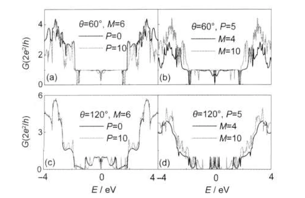
To explore size effect upon the transport properties of Zig-Zig-Zig Z-shaped GNRs,the conductances of the Z-shaped GNRs with various widths M and lengths P are shown in Fig.4. For θ=60°,it can be seen from the Fig.4(a)that with increasing P,the conductance decreases a little in high-energy region, while it changes slightly in low-energy region.In Fig.4(b),we find that the conductance of Z-shaped GNRs is highly dependent on the width M.A critical value of M=6 is obtained. Above or below the value M=6,the overall conductance decreases remarkably.These results illustrate that the conductance is maximum only for the well proportioned width Z-shaped GNRs with θ=60°.For θ=120°,it can be seen from the Fig.4(c)that with increasing P,the conductance changes a little in low-energy region,while it changes slightly in high-energy region.In addition,much more resonance tunneling peaks are observed at around EF,due to the quasibound states existing between the two corners.Similarly,much more quasibound peaks are found in Fig.4(d).Therefore,quantum dot device can be implemented by varying the length and width of GNR between the corners.
The conductance and the corresponding DOS of Zig-Arm-Zig Z-shaped GNR with θ=60°,90°,and 150°are shown in Fig.5.It can be seen that the overall conductance increases with increasing θ.A small conductance gap is observed at EFfor θ=30°and 90°,due to existing localization states between the corners.Thus the corresponding DOS peaks are observed at EF.In addition,more conductance fluctuation is observed owning to local resonance.By comparison,we find that for θ= 150°,the incident electrons can easily transmit the well proportioned Z-shaped GNR without reflection,which is because the extended states connect with each other between junction regions(not shown).No oscillations appear in the conductance at around EF.These results illustrate that the well proportioned Z-shaped GNR with θ=150°is the best conducting wire of nanocircuits.

Fig.4 Conductance of Zig-Zig-Zig Z-shaped GNRs(N=6)with various lengths P and widths M

Fig.5 Conductance and the corresponding DOS of Zig-Arm-Zig Z-shaped GNRs(N=6,M=11,P=5)with an included angle of 30°(a,b),90°(c,d),and 150°(e,f)

Fig.6 Conductance of Zig-Arm-Zig Z-shaped GNRs N=6 with various lengths Pand widths M
To further explore nanometer size effect upon the transport properties of Zig-Arm-Zig Z-shaped GNRs with θ=30°,90°, and 150°,we further calculate the conductance of Z-shaped GNRs with different widths M and lengths P(shown in Fig.6). It can be seen from Fig.6 that the conductance is highly dependent on the length P and width M.The overall conductances of Z-shaped GNRs with θ=30°and 90°decrease with increase of P and decrease of M.The back scattering increasing with P induces electron localization.The number of path between the junctions increases with M,which leads to the conductance increasing.Therefore,the length P and the width M should be considered in experiment.In the case of θ=150°,however,the varying length P almost has no effect on the conductance of Z-shaped GNRs,as shown in Fig.6(e).The conductance step remains perfectly around EF,which is similar to that of perfect ZGNR with N=6(Fig.2(a)).By varying the width M,however, much more conductance peaks are found in Fig.6(f).These peaks originate from the resonant tunneling through the quasibound state of Z-shaped GNR.The Z-shaped GNR with M=5 is similar to a double-barrier resonant structure.These results illustrate that the Z-shaped GNR with θ=150°can be used as energy filter device by modulating the width of M.In general, the well proportioned Z-shaped GNRs with θ=150°is the best conducting wire,which can be used in graphene nanocircuits.
4 Conclusions
In summary,the conductance of the Z-shaped GNRs has been explored,which is highly dependent on the geometry. The numerical results show that the conductance of the Z-shaped GNRs is highly sensitive to included angle and size of junctions.The charge density in the edge state is strongly localized on the zigzag edge sites of leads.By modulating the width of the graphene ribbons between the junctions,much more resonant peaks are observed in conductance due to quasi-bound states.The number of the resonant peaks has little to do with the length of the Z-shaped junction.Additionally,it is shown that in the low-energy region,the electrons remain ballistic transport characteristic in the width uniformity of Z-shaped GNR with included angle θ=60°or 150°.Therefore,the Z-shaped GNRs should be selected for future nanocircuit design.
(1) Hiura,H.Appl.Surf.Sci.2004,222,374.
(2) Zhang,Y.;Tan,Y.W.;Stormer,H.L.;Kim,P.Nature 2005,438, 201.
(3)Berger,C.;Song,Z.M.;Li,X.B.;Wu,X.S.;Brown,N.;Naud, C.;Mayou,D.;Li,T.B.;Hass,J.;Marchenkov,A.N.;Conrad, E.H.;First,P.N.;de Heer,W.A.Science 2006,312,1191.
(4) Berger,C.;Song,Z.M.;Li,T.B.;Li,X.B.;Ogbazghi,A.Y.; Feng,R.;Dai,Z.;Marchenkov,A.N.;Conrad,E.H.;First,P. N.;de Heer,W.A.J.Phys.Chem.B 2004,108,19912.
(5) Nakada,K.;Fujita,M.;Dresselhaus,G.;Dresselhaus,M.S. Phys.Rev.B 1996,54,17954.
(6) Ezawa,M.Phys.Rev.B 2006,73,045432.
(7) Brey,L.;Fertig,H.A.Phys.Rev.B 2006,73,195408.
(8) Li,T.C.;Lu,S.P.Phys.Rev.B 2008,77,085408.
(9) Ponomarenko,L.A.;Schedin,F.;Katsnelson,M.I.;Yang,R.; Hill,E.W.;Novolevov,K.S.;Geim,A.K.Science 2008,320, 356.
(10) Schnez,S.;Molitor,F.;Stampfer,C.;Guttinger,J.;Shorubalko, I.;Ihn,T.;Ensslin,K.Appl.Phys.Lett.2009,94,012107.
(11) Bahamon,D.A.;Pereira,A.L.C.;Schulz,P.A.Phys.Rev.B 2009,79,125414.
(12)Novoselov,K.S.;Geim,A.K.;Morozov,S.V.;Jiang,D.; Zhang,Y.;Dubonos,S.V.;Grigorieva,I.V.;Firsov,A.A. Science 2004,306,666.
(13) Echtermeyer,T.J.;Lemme,M.C.;Bolten,J.;Baus,M.; Ramsteiner,M.;Kurz,H.Eur.Phys.J.Spec.Top.2007,148,19.
(14) Russo,S.;Oostinga,J.B.;Wehenkel,D.;Heersche,H.; Sobhani,S.S.;Vandersypen,L.M.K.;Morpurgo,A.F.Phys. Rev.B 2008,77,085413.
(15) Recher,P.;Trauzettel,B.;Rycerz,A.;Blanter,Y.M.;Beenakker, C.W.J.;Morpurgo,A.F.Phys.Rev.B 2007,76,235404.
(16) Shen,T.;Wu,Y.Q.;Capano,M.A.;Robickinson,L.P.;Engel, L.W.;Ye,P.D.Appl.Phys.Lett.2008,93,122102.
(17) Xu,N.;Wang,B.L.;Sun,H.Q.;Ding,J.W.Chin.Phys.Lett. 2010,27,107303.[徐 宁,王保林,孙厚谦,丁建文.物理快报,2010,27,107303.]
(18) Xu,N.;Wang,B.L.;Sun,H.Q.;Kong,F.J.Physica B 2011, 406,756.
(19)Areshkin,D.A.;White,C.T.Nano Lett.2007,7,3253.
(20) Datta,S.Electronic Transport in Mesoscopic Systems; Cambridge University Press:Cambridge,England,1997.
(21) Xu,N.;Ding,J.W.;Xing,D.Y.J.Appl.Phys.2008,103, 083710.
(22) Xu,N.;Ding,J.W.J.Phys.:Condens.Matter 2008,48,485213.
(23) Xu,N.;Wang,B.L.;Sun,H.Q.;Kong,F.J.Chin.Phys.B 2010,19,117201.[徐 宁,王保林,孙厚谦,孔凡杰.中国物理B,2010,19,117201.]
(24) Rosales,L.;Pacheco,M.;Barticevic,Z.;latgé,A.;Orellana,P. A.Nanotechnology 2008,19,065402.
(25) Areshkin,D.A.;Gunlycke,D.;White,C.T.Nano Lett.2007,7, 204.

