
The Roadmap of 2D Materials and Devices Toward Chips
2024-04-30 08:29:14AnhanLiuXiaoweiZhangZiyuLiuYuningLiXueyangPengXinLiYueQinChenHuYanqingQiuHanJiangYangWangYifanLiJunTangJunLiuHaoGuoTaoDengSongangPengHeTianTianLingRen
Nano-Micro Letters 2024年6期
Anhan Liu, Xiaowei Zhang, Ziyu Liu, Yuning Li, Xueyang Peng, Xin Li, Yue Qin, Chen Hu, Yanqing Qiu, Han Jiang, Yang Wang, Yifan Li, Jun Tang, Jun Liu, Hao Guo✉, Tao Deng✉, Songang Peng, He Tian✉, Tian-Ling Ren✉
ABSTRACT Due to the constraints imposed by physical effects and performance degradation, silicon-based chip technology is facing certain limitations in sustaining the advancement of Moore’s law.Two-dimensional (2D) materials have emerged as highly promising candidates for the post-Moore era, offering significant potential in domains such as integrated circuits and next-generation computing.Here, in this review, the progress of 2D semiconductors in process engineering and various electronic applications are summarized.A careful introduction of material synthesis, transistor engineering focused on device configuration, dielectric engineering, contact engineering, and material integration are given first.Then 2D transistors for certain electronic applications including digital and analog circuits, heterogeneous integration chips, and sensing circuits are discussed.Moreover, several promising applications (artificial intelligence chips and quantum chips) based on specific mechanism devices are introduced.Finally, the challenges for 2D materials encountered in achieving circuit-level or system-level applications are analyzed, and potential development pathways or roadmaps are further speculated and outlooked.
KEYWORDS Two-dimensional materials; Roadmap; Integrated circuits; Post-Moore era
1 Introduction
Since the advent of integrated circuits (ICs) in 1958, their technological advancements have been driven by the relentless progression of Moore’s Law [1].The development of silicon-based complementary metal-oxide-semiconductor (CMOS) technology, from the inception of the first CPU, Intel 4004 to the advent of FinFET-based circuits, has played a pivotal role in driving the advancement of the semiconductor industry and information technology.However, as transistor dimensions have reached the nanoscale, various physical phenomena, such as thickness-fluctuation-induced scattering [2], quantum tunneling, and other short-channel effects (SCEs) [3], have emerged in silicon-based devices, causing severe performance degradation and posing challenges to the continuous advancement of Moore’s law.The conventional CMOS technology, which relies on size reduction for enhanced integration density, is now facing significant obstacles, but the demand for more powerful computing systems remains driven by rapid advances in applications like high-performance computing, Internet of Things (IoT), and artificial intelligence.
Then came the Devil once more, and put a different letter in his pocket, in which it was written that they were to put the Queen and her child to death
To foster further progress in microelectronics, three development directions have been proposed: More Moore, More than Moore, and Beyond Moore [4, 5].The More Moore path seeks to persistently scale down transistor dimensions while mitigating the detrimental effects of short-channel phenomena through innovative approaches such as novel device structures or alternative materials.The More than Moore path emphasizes the optimization of circuit design, system algorithms, and advanced packaging techniques to improve chip performance.Furthermore, it aims to diversify the functionalities of electronic systems, encompassing fields such as sensing [6], RF applications [7], flexible electronics, bioelectronics [8], and the IoT [9].The Beyond Moore direction, meanwhile, explores novel switch devices beyond traditional CMOS technology, including ferroelectric transistors [10], neuromorphic devices [11], and quantum devices [12], to realize advanced information processing capabilities.
To surmount the limitations of silicon materials and advance the development of post-Moore era, there is a need to explore novel semiconductor materials that can sustain stable and exceptional electrical properties even at reduced dimensions.2D materials, characterized by their atomic-scale thickness, have garnered significant attention.Remarkably, 2D materials exhibit noteworthy carrier mobility and gate control performance even at the ultimate limits of miniaturization [13].As a result, they have emerged as promising candidates for serving as channel materials in next-generation semiconductor devices within the More Moore domain.Furthermore, 2D materials demonstrate remarkable heterogeneity and compatibility with silicon and other 2D materials [14], allowing for seamless integration in advanced electronic systems.These materials also offer remarkable surface-to-volume ratios and surface activities, rendering them highly suitable for sensing applications within the More than Moore domain [15].Moreover, their unique quantum properties and phenomena hold considerable potential for breakthroughs in the exploration of quantum devices.In summary, 2D materials hold substantial promise for advancing Moore’s law within the More Moore, More Than Moore, and Beyond Moore directions.They offer exceptional opportunities to overcome the current limitations and push the boundaries of microelectronics technology.
At present, 2D materials encounter numerous opportunities and uncertainties.The development of mature siliconbased technology and another emerging material, carbon nanotubes (CNTs), could serve as valuable guidance and references for the advancement of 2D materials (Fig.1a).However, the progression of 2D technology experiences a certain degree of delay due to factors such as limitations in material growth.It is still a challenge to achieve circuits beyond the processor level.More expectations are being placed on the substitution of silicon in specific domains.According to IMEC’s projection, it is anticipated that by 2032, 2D materials will genuinely find application in backend-of-the-line (BEOL) processes [16].Additionally, the development of 2D materials exhibits variations across diverse application domains.To further search for the most feasible pathway toward the realization of 2D materials’ application, the proposal of a roadmap becomes essential to provide assistance and insight.
In this review, we first present an overview of the characteristics and current development status of 2D materials.Subsequently, we discuss the advancements in 2D transistor fabrication processes including material synthesis, transistor engineering, material transfer and integration, and 2D package.Then, the recent progress and applications of 2D materials in typical fields are summarized, respectively (logic chips and heterogeneous integration chips in the More Moore domain, sensor chips in the More Than Moore domain, artificial intelligence (AI) chips, and quantum chips in the Beyond Moore domain).Finally, we address some of the challenges and issues that persist in the application of 2D materials, along with highlighting the potential directions where early applications of 2D materials are most likely to be realized.
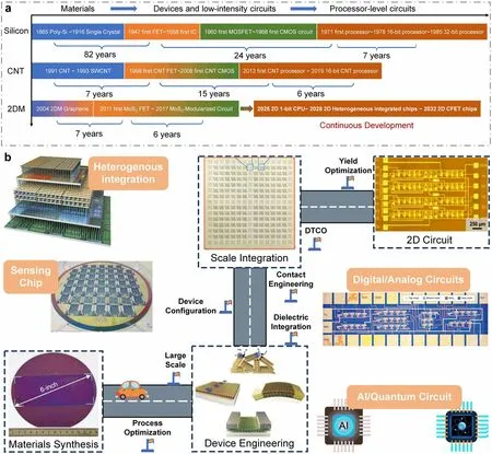
Fig.1 A schematic diagram of the general roadmap for 2D circuits.a Development timeline of silicon-based, carbon nanotube-based, and 2D ICs.b Route for the realization of 2D circuits and possible applications in the future.Reproduced with permission [17-20].Copyright (2017), (2018), (2021), (2022), Springer Nature.Reproduced with permission [21].Copyright (2023), American Chemical Society.Reproduced with permission [22].Copyright (2017), Elsevier
2 Promises of 2D Materials Toward Chips
As the most important electronic device in modern ICs, the continuous advancement of the performance of field effect transistors (FETs) has led to rapid progress in electronic technologies.To accurately assess the digital and analog performance of FETs, a set of key device parameters are defined.The fundamental basis for digital logic applications is the ability to switch transistors on and off (Fig.2a).Minimizing the off-state current (Ioff) is essential to reduce static power consumption.Achieving a large current ratio between the ON and OFF states (Ion/Ioff) exceeding 105is imperative for enhanced control accuracy.The subthreshold swing (SS) determines the switching speed of FETs.When it comes to analog applications, the intrinsic gain (Av) is one of the most important analog parameters that determines the amplification capability of a single device.However, as the technology node goes down, all these device parameters degrade severely due to the second-order effects (e.g., SCEs) in Si-based FETs, limiting its further development [23].The ideal semiconductor for sub-10-nm node should include the following features: (1) proper bandgap and excellent carrier transport properties with decreasing body thickness; (2) low defect density and good long-term stability; (3) producible in large scale, easy to integrate and compatible with Si CMOS technology [24].
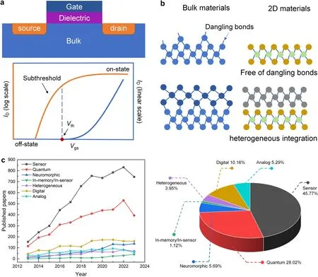
Fig.2 a Schematic of a traditional FET and typical transfer characteristic of FET device.b Partial advantages of 2D materials over bulk materials.c Number of 2D material publications from 2013 to 2023.(Keywords used for searching “two dimensional materials”, “wafer-scale OR circuit OR array” and the corresponding abbreviation for specific applications like “digital”, several typical 2D materials like MoS2 are also listed as keywords.Source: Web of Science Core Collection, accessed on January 3, 2024)
The introduction of 2D materials as the channel is an attractive strategy to address the challenges associated with scaling down.Since the first 2D materials to be discovered, graphene was isolated in 2004 [25], a broad library of 2D materials has been explored broadly including transition metal dichalcogenides (TMDCs), black phosphorus (BP), hexagonal boron nitride (h-BN), MXene and so on [26].Different from conventional bulk silicon materials, 2D materials exhibit lattice periodicity in the plane, resulting in the formation of Brillouin zones.Within this region, electron energy levels and wave functions are subject to stringent quantum constraints, allowing only specific energy levels to exist and giving rise to a quantized energy band structure.This quantum confinement effect gives 2D materials adjustable energy gaps, carrier confinement, and quantum tunneling effects.By controlling the geometry number of layers, heterostructures, etc., of 2D materials, or applying external strains, and electric fields to them, the lattice periodicity is changed, ultimately influencing the band structure and the size of the band gap.Furthermore, electrons are confined within the ultrathin body that allows excellent gate electrostatic control and has the potential of being immune to the SCEs.The mobility of 2D FETs has been enhanced to 350,000 cm2V-1s-1based on graphene prepared by chemical vapor deposition (CVD) which is accessible for wafer-scale production [27].In comparison, when the body thickness of silicon is below 5 nm, the fluctuation in material surface thickness and the pronounced scattering caused by surface dangling bonds significantly disrupt the structural periodicity of silicon [28].The buckled structure of silicene breads the atomic plane’s symmetry, unlike graphene, resulting in particularly strong Zero-Acoustic (ZA) phonon scattering [29], leading to severe mobility degradation.Furthermore, due to the surface sensitivity of silicene derived from its mixedsp2-sp3character [30], its instability in air necessitates specific preparation and usage conditions for its realization [31].
While graphene is not suitable as an active semiconductor material for electronic switching owing to its gapless band structure and graphene FETs show a limitedIon/Ioffratio leading to high power consumption in standby mode [23].Hence, graphene is usually used as metallic contact or gate materials instead of channel materials [32].In addition to graphene, MoS2, WS2, and WSe2from the family of TMDCs are developed to fabricate FETs due to their considerable bandgap (> 0.5 eV) [4].The MoS2FET with a 1-nm-wide gate electrode shows a nearly ideal SS of ~ 65 mV/decade and a largeIon/Ioffratio of ~ 106[33].The h-BN is the most common 2D insulator (Eg≈ 6 eV) and is usually considered to be the most promising gate insulator in 2D-based FETs because of the ideal interface without scattering.Efforts have also been invested in the development of novel 2D dielectric materials, like CaF2[34].The diverse lattice structures and atomic arrangements of 2D materials give rise to distinct electronic band structures, resulting in a wide energy band range, covering semimetals, semiconductors, and insulators.Besides, with the dangling-bond-free surface, the carrier mobility of 2D transistors varies little with body thickness and it is easy for 2D materials to integrate with other kinds of materials without being constrained by lattice constant matching [35].
Furthermore, with the advent of the big data era, several novel computing architectures and mechanisms have been introduced for next-generation computing technologies.Benefiting from the fascinating characteristics of 2D materials, 2D device innovation has become the focus of intense research such as 2D memory devices, neuromorphic devices, and quantum-engineering devices.2D memristor, memtransistor, flash memory, and ionic transistor are widely exploited for in-memory computing or artificial intelligence technology [11].2D materials can not only extend Moore’s Law to sub-5-nm nodes but also boost memory performance.For example, owing to the ultrathin body of 2D materials, 2D memory devices can use a low working voltage and reduce power consumption.Semi-metallic graphene was reported to be suitable as a contact material for electrodes presenting ultralow switching power or a blocking layer to inhibit efficient carrier injection due to its low density of states [36].The h-BN could be applied as the switching layer for memristive memory devices with high endurance and long retention time [37].What’s more, continuous discovery and research on novel physical mechanisms for applications in low-power switches have been proposed and investigated including tunneling transistors [38], ferroelectric transistors [39], and filament-based FET [40].Those emerging FET devices have great potential to lower the SS and subsequently lower the supply voltage and energy consumption.S.Kim et al.reported a natural heterojunction-tunneling FET with a spatially varying layer thickness in BP without interface problems.And the device’s SS has achieved a record-low level (SSave_4dec~ 22.9 mV dec-1) [38].The unique quantum properties of 2D materials also have been developed.They have strong spin-orbit coupling strength leading to enhanced Rashba effect and easier modulation of the electron spin through an externally applied electric field.The atomic-scale thickness of 2D van der Waals (vdW) heterostructure can be utilized to maximize the spin-injection efficiencies [12].And there’s plenty of application room for the computing capability drive after Moore’s law to 2D materials.
The colored lanterns had been extinguished, no more rockets rose in the air, and the cannon47 had ceased firing; but the sea became restless, and a moaning, grumbling48 sound could be heard beneath the waves: still the little mermaid remained by the cabin window, rocking up and down on the water, which enabled her to look in
3 Process Engineering for 2D Chips
Lots of efforts have been devoted to the exploration of 2D materials’ physical characteristics or device optimization.Most of the early demonstrations of 2D FETs are based on mechanically exfoliated flakes.And the research has been confined to individuals or a limited number of devices.However, to achieve circuit-level applications of 2D materials, the scale of devices should be expanded to the waferscale, which poses higher requirements on material synthesis, device processing, and integration technology.In this section, we will introduce and discuss the research progress in the field of process engineering for 2D chips.
3.1 Material Synthesis
Besides, interface modification is considered a viable strategy for mitigating contact resistance, with phase engineering gaining widespread attention due to its strong process compatibility.It has been experimentally observed that some 2D materials like MoS2, MoTe2, MoSe2, and other TMDCs demonstrate varying characteristics in different phases.Utilizing this theory, researchers have proposed phase engineering to reduce FLP and lower the Schottky barrier height (SBH).Various techniques have been proposed and investigated to induce phase transitions, including laser-induced phase patterning [102], electrostatic doping [103], argon (Ar) plasma processing [104], and so on.For instance, laser-induced phase patterning and Ar plasma handling achieve the transition of TMDCs from 2H to 1 T phase through the introduction of chalcogen vacancies.An atomically sharp interface and similar WF between 2H and 1 T phase result in a low contact resistance.Furthermore, these methods are compatible with standard lithography techniques, allowing for the formation of clean homojunctions and mitigating contamination by extraneous chemical components [102, 104].It is noteworthy, however, that some chemical processing steps can introduce defects and impurities in TMDCs [105].Additionally, it is essential to recognize that physical methods may not be readily adaptable to large-scale preparation.Moreover, in the pursuit of establishing more durable and dependable interfaces, research endeavors can be directed toward investigating approaches and mechanisms to stabilize the thermodynamically metastable phases of TMDCs [99, 105].
4.1.1 Logic Function Realization
3.1.1 Chemical Vapor Deposition
The CVD method is currently one of the most promising approaches for the direct synthesis of large-area monolayer 2D materials [41].Its advantages of low cost and scalability have sparked widespread research interest in the field of 2D materials.It has been reported that the uniform MoS2wafer size could be extended to a 12-inch diameter which is crucial for the transition of TMDC materials from laboratory research to integrated components in next-generation semiconductor devices [42] (Fig.3a).Due to the sensitivity of material growth, the substrate imperfection (e.g., grain boundaries) may lead to vacancies, impurities, wrinkles, and thickness fluctuations in the 2D sheet and the growth of polycrystalline 2D materials, which would threaten the yield and stability of devices or even result in circuit failure.
Orientation-controlled growth is considered an effective approach for achieving the preparation of WSSC TMDCs materials.By selecting a suitable substrate that matches the lattice of TMDCs, it is possible to grow TMDC films with high crystallinity, complete lattice structure, and controllable lattice orientation [54].Substrates with specific crystal orientations, such as Au(111) and sapphire (0001), have been successfully employed for the preparation of WSSC TMDCs [43, 55] (Fig.3b).L.Liu et al.reported the uniform nucleation of bilayer MoS2on c-plane sapphire.Without the transfer step, the fabricated short-channel FET devices based on bilayer MoS2exhibit an on-state current of 1.27 mA μm-1[46].
While there is another challenge that must be noted--the thermal budget.The current CVD growth methods cannot avoid the use of high temperature to achieve good crystalline, while allowable thermal budgets for the BEOL technologies are lower than 400 ℃ [56].The low growth temperature would lead to the formation of grain boundaries and stoichiometric defects in MoS2which is detrimental to lateral transport [68].The trade-off between CVD temperature and MoS2mobility determines the potential widespread adoption of CVD-based MoS2applications in the future (Fig.3c).
3.1.2 Metal-Organic Chemical Vapor Deposition
55.Forgot:Cinderella breaks her promise to leave the ball before midnight since she is busy with the prince. While forgetfulness is understandable, she does break her promise and is given a small element of humanity. The forgotten time also provides drama, causing Cinderella to run away and leave behind her shoe, providing the means for her identification later. The imagery of Cinderella s elegant clothes transforming back to rags as she runs home is a favorite scene for illustrators and filmmakers.Return to place in story.

Fig.3 a Schematic of a single 2-inch producing module unit and photograph of uniform MoS2 film with wafer sizes ranging from 2-, 4-, 8- to 12-inch.Reproduced with permission [42].Copyright (2023), Science China Press.b Schematic illustration of the MoS2 growth process on Au (111) substrate and representative μ-LEED pattern and photograph of a 1-inch uniform single-crystal MoS2 monolayer.Reproduced with permission [43].Copyright (2020), American Chemical Society.c The relation between CVD temperature and MoS2 mobility in several reports [19, 44-52].d Schematic illustration of the MOCVD process.Reproduced with permission [44].Copyright (2021), Wiley-VCH.e Optical images of exfoliated MoS2 on SiO2/Si, sapphire, and plastic film.Reproduced with permission [53].Copyright (2020), Springer Nature
Different from the CVD method, MOCVD employs metal-organic compounds as precursors and achieves uniform supply throughout the entire substrate (Fig.3d).And most 2D TMDC materials could be synthesized without the limitation of substrate constraints benefited from the strong driving force generated through pyrolysis.This enables MOCVD to achieve arbitrary combinations of various thin films and substrates [57].Additionally, MOCVD can adjust the reactant concentration by controlling the reactant partial pressures, thereby obtaining thin films with uniform electrical properties.Therefore, compared to the CVD method, the MOCVD method is more suitable for the production of high-quality, large-area 2D thin-film materials.Kang et al.reported the fabrication of 4-inch WSSC TMDC materials with high mobility (up to 30 cm2V-1s-1at room temperature) using the MOCVD method [58].Furthermore, MOCVD exhibits excellent process compatibility, enabling heterogeneous integration growth with LEDs while allowing for direct epitaxial growth at lower temperatures, making it highly compatible with CMOS technology [59].Recently, scientists from MIT have proposed a low-thermal-budget synthesis method that enables the lowtemperature rapid growth (< 300 ℃, growth time < 60 min) of single-layer MoS2with a size of up to 200 mm and a high carrier mobility of 35.9 cm2V-1s-1.This breakthrough was achieved by separating the low-temperature growth zone from the high-temperature sulfur precursor decomposition zone [46].However, the toxicity of commonly used precursors in MOCVD, like Mo(CO)6, H2S, is one of the main limiting factors for their widespread adoption, and further exploration is still required [60].
3.1.3 Mechanical Exfoliation Method
In the daytime she sat down once more beneath the windows of the castle, and began to card with her golden carding-comb; and then all happened as it had happened before
The mechanical exfoliation method is a technique that exploits the layered characteristics of 2D materials to achieve interlayer mechanical separation.The resulting 2D materials can retain a high degree of crystal structure and crystallinity, making them suitable for the preparation of small-area, high-quality single-crystal materials.Additionally, the operation and required equipment for this method are relatively simple, making it an important approach in current research for exploring novel structures or properties of 2D devices.To further increase the size of exfoliated 2D materials, enhancing the adhesion between the crystal source and substrate is a crucial prerequisite.Some noble metals, such as Au and Ni, have been proven to assist in achieving the large-area exfoliation of 2D materials [53, 61].Y.Huang et al.introduced a one-step, and universal Au-assisted mechanical exfoliation method and successfully isolated 40 types of single-crystalline monolayers, most of which are millimeter-size and high-quality [53] (Fig.3e).Although the scale of exfoliated 2D materials is extended to a considerable size, the repeatability and uniformity of the improved exfoliated method are still not guaranteed.On the other hand, the size and crystallinity of the source crystals are also critical factors limiting the scalability of the process.To achieve industrial-scale manufacturing in the future, it will be necessary to develop improved exfoliation processes and techniques for the fabrication of wafer-level single-crystal source materials.
3.1.4 Other Methods
In December 1982, I had a job at a local bank. One afternoon, we were decorating the tree in the bank lobby5 and singing carols, getting ready for the Christmas season. One of my customers approached me with a sample of her handiwork: beautiful handmade dolls. She was taking orders for Christmas. I decided6 to get one for my daughter, Katie, who was almost five years old. Then I had an idea. I asked my customer if she could make me a special doll for my mother - one with gray hair and spectacles7(): a grandmother doll.
Currently, the methodologies employed for the synthesis of WSSC monolayer TMDCs remain in a nascent stage of development.Factors such as production cost and the stability of manufacturing processes pose significant challenges, necessitating further dedicated research and optimization efforts for their prospective industrial-scale production.It is worth emphasizing that the cost-effective fabrication of WSSC 2D materials remains a formidable undertaking.However, it is crucial to acknowledge that not all applications mandate the utilization of high-quality, large-area single-crystal materials.The exceptional flexibility, high surface area, and sensitivity intrinsic to 2D materials render them suitable not only for applications in logic chip manufacturing but also for the development of flexible devices, sensors, wearable technology, and more [62].These applications exhibit relatively lower demands regarding material quality [63].Several cost-effective and scalable methods have been proposed, including liquid-phase exfoliation [64], screen printing [65], and inkjet printing [63], among others.These approaches possess the capability of waferscale fabrication, and some printing techniques facilitate patterned design as well.They offer significant advantages in terms of batch production, exfoliation efficiency, and product dimensions.
42. Red eyes, and cannot see far: Red eyes are an image associated with sorrow and with demonic fury. Eyesight is associated with mental perception, indicating that the witch s poor eyesight means poor reasoning ability, which allows Hansel and Gretel to best her (Olderr 1986). The Grimms are setting up the circumstances for Hansel and Gretel s escape from the witch.Return to place in story.
As the downsizing of transistor’s size, the decrease of gate oxide thickness is also one of the critical technologies.Unfortunately, the relatively low permittivity of SiO2(εr≈ 3.9) limits its application in FETs with gate lengths scaled down to sub-10 nm [83].Thus, novel gate dielectrics with higher dielectric constants should be developed.After decades of search for the appropriate high-k materials, Hf-based oxides, such as HfO2(κ ≈ 19), stand out as the first-generation CMOS products, which are also commonly used materials in 2D technologies [84].Whereas, considering the continuous scaling requirements and possible damage to the channel materials from the deposition process, further efforts have been devoted into the development of 2D dielectrics.2D vdW insulators, in which atomic layers are stacked via vdW interaction, are regarded as the ultimate solution for dielectric miniaturization.h-BN has been widely investigated in 2D transistors as a dielectric layer.The preparation of h-BN has achieved wafer-level and is used for device arrays [85].However, the excessive tunnel currents through ultrathin h-BN limit its further application in nanoscale 2D devices [86].Besides, several emerging 2D insulators, like CaF2, Bi2SeO5, and SrTiO3, are explored and exhibit excellent dielectric performance [34, 87, 88].For example, Zhang et al.created top-gated 2D transistors with sub-0.5-EOT dielectrics, Bi2SeO5(κ = ~ 22), and exhibit leakage current below the low-power limit of 0.015 A cm-2at 1 V gate voltage [89].Furthermore, the proper range should be estimated in conventional Si MOSFET due to the effects of both drain-induced barrier lowering and fringinginduced barrier lowering (FIBL).However, benefiting from the vdW gap between 2D semiconductors and dielectrics, the unfavorable FIBL effect is mitigated [87].
3.2 FET Engineering Approaching the Theoretical Limit
The urgent requirement for the application of 2D materials into chips boosts the research enthusiasm and development of FET engineering.Many studies have endeavored to exploit the unique structure of 2D materials for the development of novel miniaturized transistor devices, aiming to achieve the ultimate scaling of gate length or channel dimensions.Simultaneously, device performance optimization has been pursued through the optimization of dielectric layer integration and electrode integration techniques.In this part, we will elucidate the approaches for the ultimate optimization of 2D materials from three perspectives: device structure, dielectric layer integration, and contact engineering.
There was a large party at the mansion; many guests from theneighbourhood and from the capital had arrived. There were ladies with tasteful and with tasteless dresses; the big hall was quite crowded with people. The clergymen stood humbly46 together in a corner, and looked as if they were preparing for a funeral, but it was a festival-only the amusement had not yet begun. A great concert was to take place, and that is why the baron s young son had brought his willowflute with him; but he could not make it sound, nor could hisfather, and therefore the flute was good for nothing.There was music and songs of the kind which delight most thosethat perform them; otherwise quite charming! Are you an artist? said a cavalier, the son of his father; you play on the flute, you have made it yourself; it is genius thatrules- the place of honour is due to you. Certainly not! I only advance with the time, and that of courseone can t help.
3.2.1 Device Configuration
Currently, the typical structures of 2D FETs are top-gated and bottom-gated 2D FETs, which have been widely used for research on the basic properties of layered materials [13, 68].And bottom-gated 2D FETs can be further divided into global back-gated FETs and buried-gated FETs.Based on these single-gate structures, efforts have been devoted to the size scaling process.In terms of scalingLg(length of the gate electrode), Desai et al.demonstrated MoS2transistors with a 1-nm physical gate length using 1D single-wall carbon nanotube (CNT) as the gate electrode [33].Moreover, a recent report about the application of 2D single-layer graphene has scaled the Lgdown to the physical limit.The 0.34 nm thickness of graphene can be regarded as the shortestLg, which approaches the physical limit among the known materials [69].When it comes to the scaling down ofLch(length of the channel layer), diverse processing methods have been developed to decrease theLchsuch as aluminum selfoxidization technology [70], shadow evaporation method [71], crack formation [72, 73], h-BN spacer [74], and vdW metal electrodes transfer method (Fig.4) [75].R.Wu et al.demonstrated sub-100-nm-Lchbilayer tungsten diselenide (WSe2) transistors using vdW epitaxy and controlled crack formation processes.The 20-nm-long WSe2transistor shows comparable performance to silicon transistors under similar channel lengths and driving voltages [72].L.Liu et al.fabricated the sub-1-nm MoS2vertical transistors through the low-energy vdW metal integration technique.Similar to the above-mentioned graphene-gated transistors utilizing the intrinsic thickness of 2D materials, this report utilized the 0.65-nm-thick MoS2as the vertical channel layer with Ion/offof ~ 26 [75].The poor switching performance can be attributed to the SCEs and strong tunneling effect in the off-state.
To further enhance the gate-control performance of 2D transistor devices, several emerging structures applied in advanced process nodes such as double-gate FET (DGFET) [76], FinFET [77], gate-all-around FET (GAAFET) [78], and complementary FET (CFET) [79] have also been proposed in 2D technology against SCEs.Dorow et al.fabricated DGFETs by optimized atomic-layer-deposition (ALD) process for 2D material surfaces.A steep SS of 75 mV dec-1and a low DIBL of 12 mV V-1were achieved owing to the enhanced electrostatics from double gates and high-quality gate oxide layer [80].In 2022, the first GAA monolayer MoS2nanosheet FET was demonstrated by TSMC.And the performance is remarkable with 410 μA μm-1IDat 1VVDat 40 nm gate length and nearly zero DIBL that opens the path for stacked sheet GAA devices using 2D materials [78].The clean surface of 2D materials makes it an ideal candidate for 3D stacking technology in the future.When it comes to 2D FinFET, the first demonstration was fabricated by the template-growth method, while the device performance was unsatisfactory with SS obtained to be 300 mV dec-1and extracted mobilities to be in the range of 1 ~ 6 cm2V-1s-1[81].Recently, another 2D FinFET based on Bi2O2Se/Bi2SeO5epitaxial heterostructures was reported.This FinFET exhibits exciting performance including high electron mobility up to 270 cm2V-1s-1, ultralowIoffdown to ~ 1 pA μm-1, and highIon/Ioffup to 108[77].The inspiring results open up new avenues for the further extension of Moore’s law.However, it should be noted that most of these emerging structures used electron beam lithography (EBL) to pattern electrodes and channel layers, which are expensive and time-consuming.More consideration should be focused on its compatibility with Si-based processes and the feasibility of large-scale production.Simultaneously, the optimization of individual devices remains insufficient; the considerations of universality, process repeatability, and the potential for significant enhancement of integration density must also be taken into account.
All day long, I had been very busy. Picking up trash, cleaning bathrooms and scrubbing floors were all on my agenda for the day. My grown children were coming home for the weekend. I went grocery shopping and prepared for a barbeque supper, complete with ribs1 and chicken. I wanted everything to be perfect.

Fig.4 Typical strategies for ultra-scale transistors.Channel engineering: a Sub-1-nm MoS2 vertical transistors fabricated by transferred vdW metal electrodes [75].b Ultrashort vertical-channel vdW semiconductor transistors [74].c Channel defined by controlled crack formation (natural) [72].d 10 nm short channel transistor fabricated by self-oxidization of aluminum [70].e Channel defined by controlled crack formation (etching) [73].f Ultrashort MoS2 transistors fabricated by shadow evaporation [71].Gate engineering: g buried CNT gate with a diameter of 1nm [33].h Sidewall graphene edge gate with sub-1-nm thickness [69].i,j 2D FinFET and GAAFET [77, 78].k Complementary FET comprising p-type WSe2 FET and n-type MoS2 FET [79]
To achieve device size miniaturization, simultaneous progress is required in the development of complementary 2D dielectric systems in parallel with channel materials.Moreover, the atomic-level thickness channels are more sensitive to the interface with gate dielectric, which limits further improvement of device performance [82].Therefore, researches about dielectric integration of 2D FETs are focused on two aspects: One is the search for low equivalentoxide-thickness (EOT) dielectric materials, and the other one is the optimization of preparation methods and interface quality.
In summary, the fabrication of WSSC 2D materials remains a significant challenge in the current development of 2D chips.Researchers have been working on improving existing processes from various angles, including material growth mechanisms, source material selection, and process optimization, particularly in the case of CVD methods.Some progress has been made, but further enhancements are needed in terms of stability, scalability, and manufacturing cost.Additionally, unconventional growth strategies, such as geometric confinement [66] and defect engineering [16], have been proposed to address the limitations of material growth.Moreover, for applications that have relatively lower material quality requirements, some unconventional yet economically viable methods for 2D material fabrication, like printing techniques and liquid-phase exfoliation, hold promise for driving the industrialization of 2D materials [67].Therefore, it is essential to continue refining the fabrication techniques for WSSC 2D materials while promoting the development of high-performance, cost-effective, and versatile devices based on 2D materials.
To help improve 2D materials’ actual performance, the optimization of the preparation process and improvement of interface quality are another important issue.ALD is a common method to prepare a dielectric layer which has been applied in industrial production [90], while, due to the dependence of chemical reactions on surface dangling bonds and nucleation sites, corresponding requirements are put forward for the substrate materials.Considering the clean surface of 2D materials and the existence of organic residues during the transfer process, it is necessary to introduce the optimized ALD method to improve the uniformity and quality of dielectric layer growth [91].
Many interfacial activation layers and processes have been developed for the uniform deposition of high-κ oxides on 2D materials including chemical pretreatment of the surface and the introduction of a seeding layer.For example, Li et al.presented a technique to integrate ultrathin high-κ dielectric (EOT = ~ 1nm) on 2D materials using a PTCDA molecular crystal as a seeding layer.The resulting PTCDA/HfO2gate dielectric exhibits low leakage current and high breakdown field, meeting the ITRS requirement for lowpower devices [92].When selecting a seeding layer for depositing high-κ dielectrics on 2D channels, it is crucial to consider its potential impact on the properties of the channel materials.The ideal seeding layer should help form a uniform and conformal interface with the dielectric without sacrificing the performance of the channels.When it comes to the pretreatment method, functional groups and dangling bonds are introduced by using plasmas [93].Although this method avoids the introduction of additional layers, the physical plasma damage would result in the degradation of device performance attributed to bond disruption and alignments [94].In addition to ALD, several gentler integration methods are also developed to minimize the damage to 2D layers like native oxide method and the transfer of waferscale insulators [95].Certainly, the issues that need to be considered are still the scalability of methods, the uniformity of material quality, and compatibility with current Si-based technologies.
3.2.3 Contact Engineering
As a bridge connecting 2D materials with a three-dimensional system, contacts in 2D devices are one of the key aspects to be considered when exploring the electronic properties of 2D materials.The difference in electronic energy levels and lattice structures between the electrode material and 2D material leads to electron transfer and the formation of new interface states, i.e., metal-induced gap states (MIGS).The MIGS results in the Fermi level of 2D materials being pinned to a specific position, known as the Fermi level pinning (FLP).In addition, impurities and interface defects introduced by electrode deposition can also lead to substantial contact resistance.These restrict electron flow and adjustment of contact potential, leading to hysteresis or current saturation in transistor devices, the inability to achieve bipolar transport, an increase in device leakage current, and slower switching speeds [99].Therefore, achieving high-quality contacts in 2D devices is very important, which can help exhibit the expected excellent performance of 2D materials.
Currently, there are three main strategies for improving contacts: adopting novel contact materials, optimizing the interface structures, and developing new contact processes.Figure 5 summarizes some novel technologies for achieving high-quality contacts.And the development of novel contact materials is a highly active research direction for suppressing MIGS and lowering Schottky barriers in FETs.Among the various metals and semimetals, Scandium (Sc) [100], Bismuth (Bi) [97, 100], and Antimony (Sb) [101] have been successfully verified to effectively optimize the contact conditions.Specifically, Shen et al.demonstrated that the orbital resonance between Bi and MoS2, along with the near-zero density of states at Fermi level, enabled the fabrication of Bi-MoS2FETs with reduced contact resistance reduced (123 Ω μm) and improved carrier concentration (1.5 × 1013cm-2) [97].Similarly, Li et al.reported that the band structure of Sb (0112) overlaps well with MoS2, which can be further enhanced by strong vdW forces.As a result, the use of Sb as a contact material in 2D FETs led to a significant reduction in contact resistance (42 Ω μm) and a highIon/Ioffover 108.Notably, these performances outperformed equivalent silicon CMOS technologies and met the 2028 roadmap target [101].We could find that by selecting appropriate electrode materials, excellent electrical properties such as low contact resistance can be achieved.However, it is important to evaluate the stability and consider its applicability to other 2D materials.And it is crucial to take into account issues like cost and process compatibility, particularly for large-scale manufacturing.

Fig.5 Typical optimized contact strategies for 2D transistors.a Introduction of a seeding layer for contact integration or improving contact quality [92].b Doping of contact region or pretreatment of the interface [93].c VdW integration process [96].d Development of novel materials such as semi-metal contact [87, 97].e, f Novel contact modes, filament contact, and edge contact [40, 98]
Device performance consistency is a crucial foundation for achieving 2D circuits, and device performance fluctuations need to be confined within a certain range [41].In terms of material quality, the realization of chip-level 2D circuits requires the synthesis of wafer-scale single-crystal (WSSC) materials that are uniform and have low defect densities.Due to constraints related to material size, controllability, and repeatability in the fabrication process, traditional mechanical exfoliation methods are unsuitable for waferscale preparation and industrialization.In this section, we will introduce the preparation methods for wafer-scale 2D materials from various perspectives, including CVD, metal-organic chemical vapor deposition (MOCVD), mechanical exfoliation, and liquid-phase exfoliation, with a particular focus on the wafer-scale preparation of TMDCs materials.
Apart from utilizing the inherent properties of the materials, altering the mode of contact represents a methodology for optimizing contact resistance.VdW integration is thought to be a promising strategy for addressing the FLP phenomenon, which is attributed to the presence of surface dangling bonds and surface reconstructions.This integration mechanism facilitates the establishment of a physical connection between materials without direct chemical bonding.To date, several methods have been employed to realize vdW contacts, including the growth of buffer layers [106] and physical transfer techniques.For instance, Liu et al.demonstrated a method in which metal electrodes were fabricated on sacrificial substrates.Through a pretreatment procedure, the metal layers were detached from the sacrificial substrate using PMMA and then physically bonded to 2D semiconductors.This approach enabled the attainment of high carrier mobility levels that are compatible with vdW graphene hybrid contacts and strong contact doping [107].Nevertheless, it is important to highlight that as devices continue to shrink in size, achieving precise alignment between materials becomes increasingly challenging.Additionally, the weak bonding of vdW contact may lead to the deviation of metal electrodes, consequently introducing variations in device performance [108].
Except for strategies mentioned above, novel techniques have been put forward to lower the contact resistance.Notably, in 2013, Wang et al.first introduced a novel methodology that used O2and CHF3plasma etching on a BN-graphene-BN stack, followed by the deposition of metal leads at the stack’s edge, establishing direct electrode contact with the edge of graphene.This strategic configuration facilitated more efficient carrier injection in comparison with conventional top contacts, thereby yielding reduced resistance [109].Nevertheless, it is imperative to acknowledge that the stability and fabrication complexity of edge contacts present ongoing challenges [110], prompting extensive research efforts aimed at enhancing their performance, such as the combination of reactive ion etching, in situ Ar+sputtering and annealing [111] and heterostructure growth [112].Furthermore, an innovative filament contact approach has emerged as a promising avenue for achieving sub-10 mV dec-1subthreshold swing (SS) and high on-current, thus offering a novel strategy for addressing the contact resistance issue [40].
In summary, as the prerequisite for harnessing the full potential of 2D materials, realizing good electrical contacts remains the focus field of 2D technology.Numerous strategies aimed at enhancing contacts have been proposed and have yielded significant results.Nevertheless, there are still several factors that demand consideration: (1) The scalability of contact methods, assessing whether the chosen materials or techniques possess broad applicability across different types of 2D materials while remaining cost-effective; (2) Uniformity and compatibility, ensuring that the selected methods compatible with other processes, maintain device uniformity during large-scale production and support circuitlevel applications; (3) The scalability of these methods, as most research directions mentioned earlier still operate at the micrometer scale for electrode sizes.Given the ongoing trend of device size reduction, contact-related challenges will become increasingly prominent.Therefore, the development of devices with nanoscale footprints holds equal importance.
3.3 Material Transfer and Integration
A plethora of studies have reported the fabrication of 2D material-based electronic devices with excellent performance, such as low contact resistance, low leakage current, high on-state current, and shortLg[69, 72, 76].However, it remains uncertain whether such superior device performance can be replicated when scaling up to wafer-scale ICs produced through CVD.Due to the atomic layer thickness and delicate lattice of 2D materials, achieving large-scale integration of 2D devices should fully consider device yield, device-to-device variability, stability, and reliability.Such considerations must account for defects inherent to the 2D materials themselves, including vacancies, impurities, wrinkles, and thickness fluctuations, as well as external environmental factors such as changing trap states or residual organic materials.These fluctuations can result in deviations in device performance, ultimately leading to logic function errors, device failure, and decreased device yield [41].
So far, several strategies have been reported to form atomically flat interfaces and reduce the surface states from defects, residues, and strains on the 2D semiconductors.For example, to overcome the interface damage and FLP induced by high-energy metal deposition and lithography processes.Wafer-scale vdW integration method has attracted widespread attention.Liu et al.achieved vdW contact between metal and 2D semiconductor by spin-coating a decomposable poly (propylene carbonate) (PPC) as a buffer layer (Fig.6a).And this method can be readily applicable to different metals and semiconductors [113].Qi et al.demonstrated an approach of graphene-enhanced vdWs integration, which was realized by the physical transfer of 2D monolayer graphene/3D metal heterojunctions onto 2D semiconductors.The method exhibits a maximum resolution capability at the nanometer scale while yielding a device array with a near-perfect success rate of ~ 100% (Fig.6b) [96].The vdW integration method is characterized by its facile integration process, universal applicability, and capacity for enhancing device design flexibility.Nevertheless, the challenge of achieving higher alignment accuracy for small-sized electrodes and higher-density integration needs to be addressed.Moreover, the weak vdW forces demand careful consideration of potential structural deviation or performance degradation caused by subsequent processes, especially those involving high temperature.Additionally, the multiple steps of contact and release during the integration process may introduce unwanted defects or oxidation which necessitates further investigation and exploration of these issues.

Fig.6 a Wafer-scale vdW integration processes with four steps and optical images of large-scale vdW contacts.Reproduced with permission [113].Copyright (2023), Springer Nature.b Schematic illustration of graphene-enhanced vdWs integration.Reproduced with permission [96].Copyright (2023), Wiley-VCH.c Illustration of the ice-cleaning process.Reproduced with permission [114].Copyright (2023), Wiley-VCH.d Illustration of techniques and mechanism of the crack-free transfer techniques.Reproduced with permission [115].Copyright (2022), Springer Nature.e Variability analysis of multiple parameters of hundreds of MoS2 FETs.Reproduced with permission [116].Copyright (2017), American Chemical Society
In addition to the metal deposition, the presence of organic residue from polymer-assisted transfer process represents another source of defects.So far, the types of CVD growth substrates for 2D materials are still limited and the transfer process is indispensable.The most commonly used approach currently is to utilize PMMA as a supporting layer for protecting the 2D materials from tension and perturbation.And the insufficient removal of supporting polymer films will degrade the material quality [117].Better cleaning methods should be developed.Zhao et al.incorporated oxhydryl groups-contained volatile molecules into PMMA, which can be deformed under heat.The optimized supporting films could achieve a controllable conformal contact without cracks, contamination, and wrinkles (Fig.6d) [115].In addition to improvements to traditional organic-assisted transfer methods, Liu et al.proposed novel ice-aided transfer and ice-stamp transfer methods, which utilize the controllable adhesion between ice and various 2D materials.And the new transfer methods can yield ultrahigh quality and exceptional cleanliness (Fig.6c) [114].Furthermore, dielectric integration is another critical factor that affects device yield.Several researchers have attempted to adjust process steps to improve the interface quality.The gate-first process, which fabricates all the critical components before the MoS2transfer step, is believed to reduce variability effectively compared with gate-last process [118].
The integration process of 2D materials is exceedingly complex and currently immature, involving numerous process steps and parameters.On the one hand, it is necessary to establish an appropriate evaluation system to assess the impact of various parameters on device variability.Smithe et al.fabricated and measured hundreds of back-gate MoS2FETs and gave a statistical evaluation of the key parameters (Fig.6e) [116].This can aid in designing appropriate redundancy in critical parameters and structures to mitigate the effects of variability.On the other hand, it is worth considering the incorporation of machine learning techniques to assist in analyzing and optimizing the preparation process of 2D materials, assisting in the selection of optimal preparation conditions, and accelerating the iteration speed of device processes.
3.4 2D Package
Electronic packaging is one of the essential steps in chipscale integration, serving multiple functions such as signal interconnection and chip protection.However, due to the predominant focus of 2D materials research on the device level and small-scale circuits, there is still relatively limited research dedicated to the packaging of 2D chips.Considering the air sensitivity of 2D materials and their relatively limited voltage tolerance, research and development of 2D packaging technologies remain crucial.In this section, we provide a summary of the current research related to the packaging of 2D devices.
3.4.1 Signal Interconnection
Wire bonding was always used to achieve the electrical interconnection between 2D device and printed circuit board (PCB) since it was usually applied in small I/O numbers at low cost.Smith et al.[119] reported that the graphene pressure sensor and humidity sensors were wire bonded to the substrate in the ceramic dual inline package (DIP).Similar work has been reported in Susan’s work [120].They used 25-μm-thick AlSi wires to connect the optoelectronic devices based on graphene with Ti/Ag contacts to PCB.
With the I/O of devices based on 2D materials increasing, flip chip technologies can be used in the packaging of 2D devices, which needs further study on the adhesion of 2D materials on the substrate.With more I/O and high performance needed, Chiplets [121], 2.5-dimensional integration [122], and three-dimensional integration [123] can also be adopted to achieve the large-scale integration and improve the integration density.
3.4.2 Chip Protection
Protecting layer before packaging: Compared to the traditional semiconductors, most 2D materials exhibit heightened sensitivity to water and oxygen when they are exposed to the ambient air owing to their elevated surface-to-volume ratio [124].For example, it has been demonstrated that BP is highly reactive to oxygen and water exposed to ambient air, leading to degradation in the electronic and optical properties [125].Consequently, the encapsulation strategies for 2D materials discussed in the work involve the creation of a protective layer that isolates 2D material from oxygen and water in the air to prevent the reaction.
The protecting layer encapsulated on 2D materials is primarily divided into organic and inorganic protective layers.Polymethyl methacrylate (PMMA) [126], polyvinyl pyrrolidone (PVP) [127], fluoropolymer CYTOP [128], and parylene C [129] were commonly used as the organic protective layers to protect 2D materials.For example, Jia et al.[130] and Li et al.[131] reported that the PMMA-encapsulated BP FETs exhibit high stability over several weeks and achieve a high field-effect mobility up to 1150 cm2V-1s-1.Besides PMMA, the other organic materials also process the same function to protect 2D materials in ambient air.
Besides organic protective layer, the inorganic protective layer was commonly used to protect 2D materials.Oxide (Al2O3) [132], zirconium oxide (ZrO2) [133], and hafnium dioxide (HfO2) [134] were the most widely materials with the deposition process of atomic layer deposition (ALD).For example, Li et al.[135] directly encapsulated MoS2FETs with Al2O3by ALD, and then, the MoS2-based FETs had a high Ion/Ioffratio exceeding 108and the mobility around 70 cm2V-1s-1at room temperature.ZrO2and HfO2are also used to protect h-BN and MoS2to improve the device’s performance.
Other protections in the packaging and its perspective:When 2D devices are used in the high-performance memory, molding compound as the package must be used in the future.However, there is still a relatively limited amount of research.Effects of the warpage and stress during the molding process on the 2D devices are worthy of deep studying.
Electrostatic discharge (ESD) protection is another concern for the packaging of 2D devices.The nano-electronicsbased 2D materials process highIon/Ioffratios in FETs [13] and band gap tunability [136]; thus, it has been widely used in low-power transistors [137], sensors [138], and photodetectors [139].Meanwhile, the 2D materials also can withstand high breakdown voltage.For example, the breakdown voltage of MoS2semiconducting gate (SG) FET is 408 V [140].Thus, 2D devices provide a large design window for ESD protection.
However, there is a lack of strategies for ESD protection of 2D devices.Thus, we make prospects of ESD protection way based on Si devices: firstly, designing a switch around the device that can be precisely controlled such as a nanophase-switch [141] and gNEMS ESD switch [142] and secondly designing a protection structure in the PCB to discharge any ESD transients such as setting a mixed-mode ESD protection circuit [143] and dual-polarity nano-crossbar array ESD protection structure [144] of the device based on 2D materials.It is worth noting that 2D materials can withstand high breakdown voltage; thus, their ESD protection can be installed on PCB.
With the development of devices based on 2D materials, their package become more important for application.Therefore, we need more research on package of devices based on 2D materials to achieve the holistic development of 2D materials application.
4 2D Materials for Digital and Analog Chips
Integrated circuit (IC) technology breaks the separation of devices and wires in traditional electronic technology, leading the trend of electronic components and lines and even the whole system toward integration [1].Among all kinds of circuits, digital and analog circuits are the two main streams.Compared to bulk silicon, the ability to achieve extremely thin
- Nano-Micro Letters的其它文章
- Publisher Correction to: Strongly Coupled 2D Transition Metal Chalcogenide-MXene-Carbonaceous Nanoribbon Heterostructures with Ultrafast Ion Transport for Boosting Sodium/Potassium Ions Storage
- Dual-Atom Nanozyme Eye Drops Attenuate Inflammation and Break the Vicious Cycle in Dry Eye Disease
- Highly Aligned Graphene Aerogels for Multifunctional Composites
- All-Covalent Organic Framework Nanofilms Assembled Lithium-Ion Capacitor to Solve the Imbalanced Charge Storage Kinetics
- Thioacetamide Additive Homogenizing Zn Deposition Revealed by In Situ Digital Holography for Advanced Zn Ion Batteries
- Janus Quasi-Solid Electrolyte Membranes with Asymmetric Porous Structure for High-Performance Lithium-Metal Batteries