Superconducting joints using reacted multifilament MgB2 wires: A technology toward cryogen-free MRI magnets
Dipk Ptel ,Akiyoshi Mtsumoto ,Hiroki Kumkur ,Yuk Hr ,Toru Hr ,Minoru Med ,Ho Ling,Yusuke Ymuhi,Seyong Choi,Jung Ho Kim,Md Shhrir A.Hossin
aSchool of Mechanical and Mining Engineering, The University of Queensland, St Lucia, Queensland 4072, Australia
b National Institute for Materials Science (NIMS), 1-2-1 Sengen, Tsukuba, Ibaraki 305-0047, Japan
c Department of Electrical Engineering and Kangwon High Magnetic Field Center, Institute of Quantum Convergence Technology, Kangwon National University, Gangwon 24341, Republic of Korea
d Australian Institute for Bioengineering and Nanotechnology (AIBN), The University of Queensland, St Lucia, Queensland 4072, Australia
e Department of Materials Process Engineering, Graduate School of Engineering, Nagoya University, Nagoya, Aichi 464-8603, Japan
fInstitute for Superconducting and Electronic Materials, Australian Institute for Innovative Materials, University of Wollongong, North Wollongong, New South Wales 2500, Australia
Abstract The development of superconducting joining technology for reacted magnesium diboride (MgB2) conductors remains a critical challenge for the advancement of cryogen-free MgB2-based magnets for magnetic resonance imaging (MRI).Herein,the fabrication of superconducting joints using reacted carbon-doped multifilament MgB2 wires for MRI magnets is reported.To achieve successful superconducting joints,the powder-in-mold method was employed,which involved tuning the filament protection mechanism,the powder compaction pressure,and the heat treatment condition.The fabricated joints demonstrated clear superconducting-to-normal transitions in self-field,with effective magnetic field screening up to 0.5 T at 20 K.To evaluate the interface between one of the MgB2 filaments and the MgB2 bulk within the joint,serial sectioning was conducted for the first time in this type of superconducting joint.The serial sectioning revealed space formation at the interface,potentially caused by the volume shrinkage associated with the MgB2 formation or the combined effect of the volume shrinkage and the different thermal expansion coefficients of the MgB2 bulk,the filament,the mold,and the sealing material.These findings are expected to be pivotal in developing MgB2 superconducting joining technology for MRI magnet applications through interface engineering.
Keywords: MgB2 superconducting joint;MgB2 conductor;MRI applications;Cryogen-free magnet;Persistent-mode operation.
1.Introduction
Magnetic resonance imaging (MRI) is a medical diagnostic device that helps doctors to examine body organs noninvasively.High-resolution scans of body parts in an MRI are formed using a strong and uniform magnetic field,and radio waves.The powerful and uniform magnetic field needed for forming an MRI scan in an MRI bore is usually generated using several niobium-titanium (Nb-Ti) superconducting coils cooled in expensive liquid-helium (LHe) as schematically shown in Fig.1(a) [1].Over the years,helium price has been continuously increasing and supply issues are common[1–5].High device and installation costs of well over a million dollars and a high maintenance cost restrict smaller diagnostic centers from having an MRI scanner in metropolitan or rural areas [3,6].Therefore,the development of a cryogen-free cost-effective MRI scanner is crucial for making this critical diagnostic tool widely available to serve communities around the globe.

Fig.1.(a) Artist’s 3D model of an MRI scanner.(b) Schematic illustration of a superconducting MRI magnet assembled using multiple superconducting coils,joints,and a PCS.
Philips has made significant progress in this direction by developing a fully sealed magnet known as the BlueSeal magnet which only requires 7 liters (L) of LHe to cool an Nb-Ti MRI magnet at 4.2 K [7].GE is also developing a similar technology known as Freelium Technology,which is expected to use 20 L of LHe to cool their fully sealed Nb-Ti MRI magnet at 4.2 K [8].However,to eliminate the requirement to use LHe altogether to cool an MRI magnet,the magnesium diboride (MgB2) superconductor,which has a critical temperature (Tc) of 39 K is known to be the frontrunner [9–20].In fact,ASG Superconductor’s Paramed MRI unit has developed an MRI scanner using a cryogen-free 0.5 T MgB2MRI magnet cooled at 20 K by cryocoolers [21].Despite the numerous benefits of using an MgB2magnet in an MRI [22],the commercial acceptance of the Paramed’s MROpen system is still limited [23].Among several reasons for poor acceptance in the medical industry,one of the reasons could be the mode of operation of its magnet system.
Usually,an Nb-Ti MRI magnet is assembled using multiple coils and each coil is connected with another coil using two‘superconducting joints’ [24],and the ends of the magnet are connected using a persistent-current switch (PCS,a superconducting coil wound in a noninductive fashion) and two superconducting joints to form a closed loop as shown in Fig.1(b).The PCS allows charging the magnet by inducing a finite resistance across the magnet via an inbuilt heater.Once the magnet is charged and the heater is turned off,the current flows in the closed loop producing the necessary ultra-stable magnetic field (<0.1 ppm h-1decay rate) [1].This mode of magnet operation is called the persistent-mode operation.The MgB2magnet of the Paramed’s MROpen MRI scanner is not operated in persistent mode,since the MgB2superconducting joining technology has not been fully developed yet.Therefore,the development of superconducting joining technology is crucial for the advancement of MgB2-based cryogen-free MRI magnets [25].
Since the first report of superconducting joining between an unreacted monofilament MgB2wire and an Nb-Ti wire in 2005 [26],many superconducting joints have been fabricated using both monofilament [11,15,27-43]and multifilament MgB2conductors [27,29,44-51].Most of these joints were fabricated using unreacted MgB2conductors with few exceptions,in which reacted MgB2conductors were used[27,38,45,52].MgB2coils for MRI magnets are expected to be manufactured using a reacted multifilament MgB2conductor to minimize modification in the existing manufacturing processes used for Nb-Ti-based MRI magnets [9,53].This means a superconducting joining technique must be developed that can be used to fabricate joints between reacted multifilament MgB2conductors.Moreover,carbon (C)-doped boron(B) powder is often used as a precursor for manufacturing MgB2conductors,since C impurity in MgB2material helps to improve the performance of MgB2conductors in high magnetic fields [14,54-58].However,a joint fabrication using Cdoped MgB2conductors is found to be much more difficult compared with un-doped conductors due to unknown reasons[29,33].Furthermore,the MgB2-based MRI magnet is expected to be operated at around 20 K to take full advantage of the high cooling capacity of cryocoolers around 20 K.For example,the Cryomech-made single-stage Gifford-McMahon AL630 cryocooler model has a cooling capacity of 100 W at 20 K,whereas their two-stage pulse tube PT450 cryocooler model has a cooling capacity of 5 W at 4.2 K on its 2ndstage and 65 W at 45 K on its 1ststage [59].No superconducting joint results have been reported to date using reacted C-doped multifilament MgB2conductors at 20 K despite the fact that this is the type of MgB2conductor that is considered to be nearly fulfilling the requirements for a cryogen-free MRI magnet [9].
To overcome this challenge,for the first time,we report superconducting joints fabricated using reacted C-doped multifilament MgB2wires for MRI magnet applications.To realize a low-temperature reaction between Mg and C-doped B to form an MgB2bulk and simultaneous MgB2to MgB2interface,the powder-in-mold method was employed by concurrently tuning filaments protection mechanism in and out of the mold,the powder compaction pressure,and the heat treatment condition.The fabricated superconducting joints were evaluated in detail for their transport,compositional,and microstructural properties.To further evaluate the interface between one of the MgB2filaments and the MgB2bulk within the joint,the serial sectioning was carried out for the first time in this type of superconducting joint.
2.Experimental procedures
A multifilament MgB2wire (C-doped andin situ) for this work was produced using the continuous tube forming and filling (CTFF) process [60].Table 1 shows the specifications of the MgB2wire.A variable temperature insert (VTI) in a superconducting magnet was used to evaluate the critical currents (Ic(s)) of the wire and the joints in different magnetic fields and temperatures.To estimate theIc(s) of the wire and the joints in a four-probe measurement setup,the criterion of 1 μVcm-1was utilized.Fig.2(a) shows theIcmeasurement probe for the joints.TheTcof the joint was evaluated by employing the four-probe method in a gas exchange type cryostat.Fig.2(b) shows theTcmeasurement probe.

Table 1 Specifications of the multifilament MgB2 wire.The multifilament MgB2 wire used in the study was first heat-treated at 650°C for 1 h before the fabrication of the joints.The joints were then heat-treated for 3 h at 640°C.To compare the performance of the joints with the wire,the wire was heat-treated for a total of 650°C/1h+640°C/3h before measuring the Ic data.
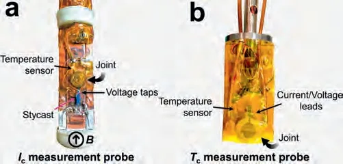
Fig.2.(a) Photograph of the Ic measurement probe for the joints.(b) Photograph of the Tc measurement probe.The probe was used to measure the resistance of the joint at different temperatures by applying a constant direct current (DC) of 10 mA.The top portion of the joint was cut to fit it within the cryostat’s bore.
An X-ray diffraction (XRD) machine,Rigaku Miniflex II was employed to obtain an XRD pattern for the joint’s structural analysis;to determine the mole fraction from the XRD data,the Rietveld refinement tool,RIETAN-FP was used[11,61];for taking scanning electron microscope (SEM) images and energy dispersive X-ray spectroscopy (EDS) maps,a Hitachi SU-70 SEM was used;for focused ion beam (FIB)sample preparation,EDS mapping,the serial sectioning,and SEM images,an FIB-SEM (SMF-1000,Hitachi Hi-Tech Corporation) was used [62].
3.Results and discussion
For fabricating the superconducting joints,the procured MgB2wire was first heat-treated at 650°C for 1 h in an inert argon (Ar) atmosphere to form MgB2in it.Then,the joints were fabricated using this reacted C-doped multifilament MgB2wire.Since the joint fabrication process required the joints to be heat-treated at 640°C for 3 h,the wire was heat-treated for a total time of 650°C/1h+640°C/3h for measuring theIc(s).TheIc(s) of the wire at 20 K in various magnetic fields are shown in Fig.3(a).A cross-section of the MgB2wire is shown in the inset.Fig.3(b) shows the current-dependent electric fields at 20 K in various magnetic fields.
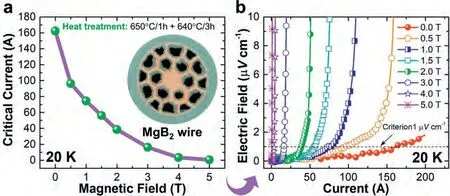
Fig.3.(a) Critical current of the wire at 20 K in various magnetic fields.Inset: A cross-section of the MgB2 wire.(b) Current-dependent electric fields at 20 K in various magnetic fields.
Fig.4(a) schematically shows our superconducting joining process to connect two reacted C-doped multifilament MgB2wires.Copper (Cu) and Monel react with Mg in the course of the heat treatment.Hence,to remove Cu and Monel,nitric acid (HNO3,60% w/w,0.5 h) was utilized to etch the ends of the wires first followed by an angle (10°) cutting [49].Angle cutting increased the exposed area of the MgB2filaments for joining.For wire cutting,an automated cutting machine without any cutting fluid was used (Cutting: 0.64 mm thick diamond disk,Speed: 1 mm min-1,Rotation: 4000 rpm).A stainless steel (SS) mold with two holes on one side was used for the joint fabrication.Table 2 shows the specifications of the mold.In the following step,a base(thickness:∼0.71 mm)was prepared using a mixture of Mg and C-encapsulated B as per the stochiometric ratio of MgB2in an Ar glovebox(compaction pressure: 199 MPa) [49].In the next step,previously prepared two reacted MgB2wires were placed on the base in such a way that only the etched portion of the wires remained inside the mold cavity.
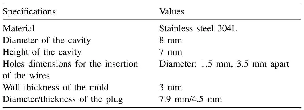
Table 2 Specifications of the mold and the plug.
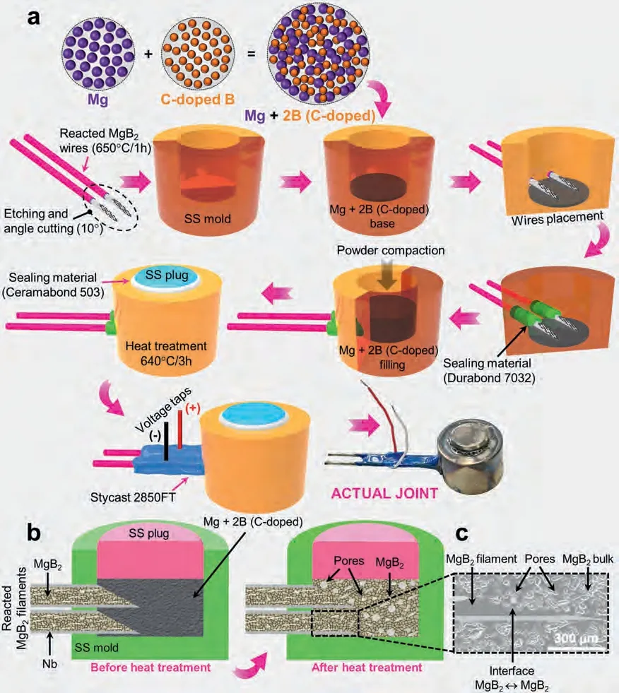
Fig.4.(a) Joint fabrication steps for reacted C-doped multifilament MgB2 wires.(b) Joint cross-section illustration before and after the heat treatment.(c)Cross-sectional SEM image of the interface between one of the MgB2 filaments and the MgB2 bulk in joint 2.Powder specifications: Mg (Alfa Aesar,99.8%,-325 mesh) and B (Pavezyum,4.1 at% C-encapsulated)
Next,in the open air,Durabond 7032 (a high-temperature sealing material with a maximum operating temperature of 1093°C) [63]was applied inside,in the holes,and outside of the mold to secure the wires.Note that the application of the sealing material inside the mold is crucial to protect the reacted wires from damage due to vertical pressure.The sealant was allowed to cure for 24 h in the open air.After the curing process,the joint was moved to the Ar glovebox,filled using the same Mg+2B mixture used for the base,and compacted using the specific pressure listed in Table 3.An SS plug was set on the bulk and sealed using Ceramabond 503(a high-temperature sealing material with a maximum operating temperature of 1650°C) [64].Following 24 h curing of the sealing material,the joint was heat-treated at 640°C for 3 h in an Ar atmosphere.In all the heat treatment processes,5°C min-1ramp-up and the cool-down rate were used.Following the heat treatment of the joint,voltage taps were soldered on the wires.To protect the wires from damage during handling and measurement,Stycast 2850FT prepared using Catalyst 9 was applied and cured for 24 h.Using this method and by applying two different compaction pressures as mentioned in Table 3,two joints (Joint 1: 39.8 MPa,Joint 2: 59.7 MPa)were fabricated.Fig.4(b) shows the joint cross-section illustration before and after the heat treatment.Fig.4(c) shows a cross-sectional SEM image of the interface between one of the MgB2filaments and the MgB2bulk in joint 2.Pores formation was observed in the MgB2bulk as a result of diffusion of Mg to B sites.

Table 3 Specifications of the joints.
Fig.5(a) shows the photograph of the fabricated superconducting joint using the reacted C-doped multifilament MgB2wires.Firstly,as shown in Fig.5(b),theIc(s) of both joints were measured at various temperatures in self-field.Joint 2 made using 59.7 MPa pressure showed better performance in comparison to joint 1.Joints 1 and 2 reachedIcvalues of 20.9 A and 17.9 A,respectively at 20 K in self-field.Current-dependent electric fields in self-field at various temperatures of both joints are shown in Figs.5(c) and 5(d).Clear superconducting-to-normal transitions were observed in both joints at different temperatures.
Once theIc(s) of the joints were evaluated in self-field,in the next step,theIc(s) of the joints were evaluated at 20 K in various magnetic fields.Since this type of joint architecture can show the effect of a magnetic field screening as previously reported by us [49],theIc(s) of the joints were first measured from a low to a high field at 20 K as shown in Fig.6(a).Corresponding current-dependent electric fields are shown in Figs.7(a) and (b).As can be seen in Fig.6(a),both the joints showed a magnetic field screening effect up to 0.5 T,because the reduction in theIc(s) values were only about 7%and 6% for joints 1 and 2,respectively from self-field to 0.5 T field at 20 K.Beyond 0.5 T,theIc(s) of the joints were rapidly decreased.The current retention ratio of joint 2 in 0.5 T at 20 K is about 20% compared with the bare wire,which needs improvement for practical applications.Since this is preliminary work,further optimization would be possible to improve the performance of the joints.

Fig.6.Magnetic field dependent critical currents of the joints at 20 K.(a) For this Ic(s) measurement,the magnetic field was increased from a low to a high field by keeping a constant temperature of 20 K.(b) For this Ic(s) measurement,the magnetic field was increased from a low to a high field.Before each in-field Ic measurement,the temperature of the joint was raised more than the Tc before cooling down to 20 K.
To confirm that both joints demonstrated a magnetic field screening effect during the process of measuring theIc(s)from low to high fields,a different approach was taken in the next step as illustrated in Fig.6(b).TheIc(s) of the joints were measured by increasing the magnetic field from a low to a high value.However,before each in-fieldIcmeasurement,the joint’s temperature was raised above theTcvalue and then cooled down to 20 K.As a consequence,some amount of magnetic field was trapped in the joints [49].Therefore,when theIc(s) of the joints were re-measured,the reduction in theIc(s) values was about 44.5% and 46.7%for joints 1 and 2,respectively from self-field to 0.5 T field at 20 K.These findings indicate that both joints exhibited a magnetic field screening effect during theIc(s) measurements conducted at a constant temperature while increasing the magnetic field from low to high.Current-dependent electric fields for these measurements are shown in Figs.7(c)and (d).
Due to its better performance in comparison to joint 1,joint 2 was selected for further analysis of itsTcin selffield,as illustrated in Fig.8(a).The measuredTcof joint 2 was ∼32.8 K.Reduction inTcvalue is usually observed in C-doped MgB2material [50].To further carry out the XRD and microscopy,the joint was cut from a specific location as shown in Fig.8(b).A half side was used to extract a powder sample for XRD analysis and the other part was used for conducting microscopy.As depicted in Fig.8(c),an XRD pattern was obtained for a powder sample extracted from joint 2.Despite the presence of the sealing material within the cavity (as shown in Fig.4(a)),the primary phase identified in the XRD pattern was MgB2(95.5 mol%),with a second minor phase of magnesium oxide (MgO,4.5 mol%).A small amount of MgO formation is common in MgB2material due to contamination of Mg during handling [49,53].
After conductingTcand XRD evaluations,further analysis was performed on the microstructural characteristics of joint 2.SEM images of one of the MgB2filaments present within joint 2′s cross-section at varying magnifications are illustrated in Figs.8(d) to (g).As can be seen in Fig.8(d),the base height (see Fig.4(a)) of the MgB2bulk was ∼0.71 mm.A slightly high magnified SEM image was taken around the MgB2filament core and bulk interface as shown in Fig.8(e).The selected location in Fig.8(e) was further observed as shown in Fig.8(f) to see the area around the interface more closely.As can be seen in the figure,many voids were formed in the MgB2bulk near the interface.Fig.8(g) demonstrates that the interface between the filament and bulk of joint 2 appeared to be well-formed,without any noticeable cracks or defects.Corresponding EDS maps of the location shown in Fig.8(g)are shown in Fig.9.The defect-free interface implies that the performance of the joint should be much better than what has been measured.To investigate this point further,an FIB was employed to study the cross-section of the interface in the thickness direction.

Fig.9.(a) SEM image of the selected area of interface between one of the MgB2 filaments and the bulk within joint 2’s cross-section (as shown in Fig.8(g)).EDS maps of (b) Mg,(c) B,(d) O,and (e) Nb acquired from the location shown in Fig.9(a).
Figs.10(a) and (b) illustrate the FIB cutting location to pick up a sample for further analysis.A tilted (55.5°) SEM image of the interface is depicted in Fig.10(c) after removing the material from one side,while Fig.10(d)displays the SEM image of the interface between the MgB2bulk and the filament from the indicated location with an orange arrow.The yellow arrows in Fig.10(d) indicate a visible space at the interface,which is thought to be responsible for the joints’inferior performance.To gain a deeper understanding of the interface,material from the other side was removed using the FIB,as shown in Fig.10(e).Moreover,SEM,EDS,and the serial sectioning were conducted on the side shown in Fig.10(e).
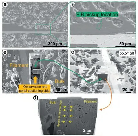
Fig.10.(a) SEM image of the interface between one of the MgB2 filaments within joint 2’s cross-section and the bulk.(b) SEM image of the selected area is shown in Fig.10(a) and the FIB pickup location.(c) Tilted (55.5°) SEM image of the interface after removing the material from one side.(d) SEM image of the interface between the MgB2 bulk and the filament from the location shown via an orange arrow.Space at the interface is marked by several yellow arrows.(e) SEM image of the location from where the interface observation and the serial sectioning were conducted.
Fig.11(a) shows an SEM image of the sample extracted using the FIB from the interface shown in Fig.10(e).Fig.11(b) shows a higher magnification image of the selected area in Fig.11(a).The left side of the interface represents the MgB2filament,while the right side is the MgB2bulk.The filament contains a large number of pores compared to the bulk,as shown by black arrows.A visible spacing of up to ∼0.98 μm wide can also be observed at the interface.The filament appears to be weakly connected to the bulk at some locations,but clear space is visible in most areas.This spacing could be responsible for the joint’s inferior performance.

Fig.11.(a) SEM image of the sample picked up using the FIB from the location shown in Fig.10(e).(b) SEM image of the area shown in Fig.11(a).(c)Reference SE image for EDS mapping.EDS maps of (d) B,(e) O,and (f) Mg taken from the area shown in Fig.11(c).(g) Selected SEM images while performing the serial sectioning using the FIB.Each slide was taken at an average 15.0 ± 0.1 nm depth.(h) 3D reconstructed model from the images taken during the serial sectioning.
This space could have potentially formed due to the volume shrinkage(up to 25%)caused by the Mg+2B →MgB2reaction [65]or the combined effect of the volume shrinkage and the different thermal expansion coefficients (α) of the MgB2bulk (41.4×10⁻⁶K-1at 20°C and 68.0×10⁻⁶K-1at 640°C) [66],the constituent materials of the filament such as Nb (7.0×10⁻⁶K-1at 20°C and 8.2×10⁻⁶K-1at 640°C) [67]and MgB2,the stainless steel mold (15.3×10⁻⁶K-1at 20°C and 20.6×10⁻⁶K-1at 640°C,these properties are of SS304) [68],and the high-temperature sealing material Durabond 7032 (16.2×10⁻⁶K-1at room temperature (RT))[63].This spacing was likely formed during the reaction process because if it had formed during the cryogenic cooling process,the morphology of the space would be more like a crack.This observation implies that the space was unlikely formed due to the cryogenic epoxy Stycast 2850FT (αof 35.0×10⁻⁶K-1at RT) [69]or the high-temperature sealing material Ceramabond 503 (αof 7.2×10⁻⁶K-1at RT)[64]pasted on the top of the mold.To improve the joint’s performance,this spacing needs to be eliminated.
The interface shown in Fig.11(c) was further analyzed using EDS mapping as shown in Figs.11(d) to (f).EDS map of the O shows that O content in the filament was notably high compared with the bulk.This means the filament could have been contaminated during etching using HNO3.Similar contamination was observed in our previous work [49].Thus,the etching process must be optimized to minimize contamination to improve the performance of the joint.Furthermore,to observe microstructure in the z-direction,the serial sectioning was conducted.Fig.11(g) shows selected slides collected during the serial sectioning.A total of 992 slides were collected from a 14.9 μm thickness volume,which resulted in an average slide thickness of 15.0 ± 0.1 nm.As can be seen in the supplemental movie 1 produced using the slides,there is a varying amount of spacing throughout the depth of the specimen.Fig.11(h)shows the three-dimensional(3D)reconstructed model using the slides.The reconstructed model also shows the spacing throughout.Our findings are expected to play a pivotal role in carrying out interface engineering toward the development of MgB2superconducting joining technology for MRI magnet applications.
4.Conclusions
We have successfully fabricated superconducting joints for MRI magnet applications using reacted C-doped multifilament MgB2wires for the first time.Our power-in-mold method involves a low-temperature reaction between Mg and C-doped B to form an MgB2bulk and simultaneous MgB2to MgB2interface with the filaments protection mechanism in and out of the mold,the low powder compaction pressure,and 640°C for 3 h heat treatment condition.Joint 2 exhibited anIcvalue of 17.9 A at 20 K in 0.5 T,aTcof ∼32.8 K in self-field,and a strong magnetic field screening effect up to 0.5 T at 20 K.The XRD pattern of joint 2 revealed a predominant phase of MgB2(95.5 mol%) with a minor MgO (4.5 mol%) phase,despite the presence of sealing material inside the mold cavity.The initial cross-sectional SEM imaging of joint 2 showed a wellformed interface between the filament and the bulk without any visible defects.However,a sample picked up from the interface location using the FIB showed spacing,which was expected to be formed due to the volume shrinkage caused by the Mg+2B →MgB2reaction or the combined effect of the volume shrinkage and the different thermal expansion coefficients of the MgB2bulk,the filament,the mold,and the sealing material.To improve joint performance,this spacing needs to be eliminated.
Declaration of competing interest
The authors declare that they have no known competing financial interests or personal relationships that could have appeared to influence the work reported in this paper.
CRediT authorship contribution statement
Dipak Patel:Conceptualization,Data curation,Formal analysis,Funding acquisition,Investigation,Methodology,Validation,Visualization,Writing– original draft,Writing– review &editing.Akiyoshi Matsumoto:Formal analysis,Funding acquisition,Project administration,Resources,Supervision,Validation,Writing– review &editing.Hiroaki Kumakura:Validation,Writing– review &editing.Yuka Hara:Investigation,Validation,Writing– review &editing.Toru Hara:Investigation,Validation,Visualization,Writing– review &editing.Minoru Maeda:Formal analysis,Validation,Visualization,Writing– review &editing.Hao Liang:Validation,Writing– review &editing.Yusuke Yamauchi:Validation,Writing– review &editing.Seyong Choi:Validation,Writing– review &editing.Jung Ho Kim:Validation,Writing– review &editing.Md Shahriar A.Hossain:Funding acquisition,Validation,Writing– review &editing.
Acknowledgement
This work was supported by the Japan Society for the Promotion of Science (JSPS) KAKENHI Grant Number JP18F18714,and Cryogenic Station,Research Network and Facility Services Division,National Institute for Materials Science (NIMS),Japan.This work was also supported by the ARC Linkage Project(LP200200689).The experimental work presented in this manuscript was carried out by Dipak Patel while working at NIMS,Japan,and analyzed at UQ,Australia.The manuscript was organized by Dipak Patel while working at UQ/CSIRO,Australia.
Supplementary materials
Supplementary material associated with this article can be found,in the online version,at doi:10.1016/j.jma.2023.11.014.
 Journal of Magnesium and Alloys2024年1期
- Journal of Magnesium and Alloys的其它文章
- Graphene–calcium carbonate coating to improve the degradation resistance and mechanical integrity of a biodegradable implant
- Degradable magnesium alloy suture promotes fibrocartilaginous interface regeneration in a rat rotator cuff transosseous repair model
- Stress-corrosion coupled damage localization induced by secondary phases in bio-degradable Mg alloys: phase-field modeling
- HVOF-sprayed HAp/S53P4 BG composite coatings on an AZ31 alloy for potential applications in temporary implants
- Greatly enhanced corrosion/wear resistances of epoxy coating for Mg alloy through a synergistic effect between functionalized graphene and insulated blocking layer
- Superplasticity of fine-grained Mg-10Li alloy prepared by severe plastic deformation and understanding its deformation mechanisms
