
Moderate Fields, Maximum Potential: Achieving High Records with Temperature-Stable Energy Storage in Lead-Free BNT-Based Ceramics
2024-03-22 08:46WenjingShiLeiyangZhangRuiyiJingYunyaoHuangFukangChenVladimirShurXiaoyongWeiGangLiuHongliangDuLiJin
Nano-Micro Letters 2024年5期
Wenjing Shi, Leiyang Zhang, Ruiyi Jing, Yunyao Huang, Fukang Chen, Vladimir Shur, Xiaoyong Wei, Gang Liu✉, Hongliang Du, Li Jin✉
ABSTRACT T h e increasing awareness of environmental concerns has prompted a surge in the exploration of leadfree, high-power ceramic capacitors.Ongoing efforts to develop leadfree dielectric ceramics with exceptional energystorage performance (ESP) have predominantly relied on multicomponent composite strategies, often accomplished under ultrahigh electric fields.However, this approach poses challenges in insulation and system downsizing due to the necessary working voltage under such conditions.Despite extensive study, bulk ceramics of (Bi0.5Na0.5)TiO3 (BNT), a prominent lead-free dielectric ceramic family, have seldom achieved a recoverable energy-storage (ES) density (Wrec) exceeding 7 J cm-3.This study introduces a novel approach to attain ceramic capacitors with high ESP under moderate electric fields by regulating permittivity based on a linear dielectric model, enhancing insulation quality, and engineering domain structures through chemical formula optimization.The incorporation of SrTiO3 (ST) into the BNT matrix is revealed to reduce the dielectric constant, while the addition of Bi(Mg2/3Nb1/3)O3 (BMN) aids in maintaining polarization.Additionally, the study elucidates the methodology to achieve high ESP at moderate electric fields ranging from 300 to 500 kV cm-1.In our optimized composition, 0.5(Bi0.5Na0.4K0.1)TiO3—0.5(2/3ST-1/3BMN) (B-0.5SB) ceramics, we achieved a Wrec of 7.19 J cm-3 with an efficiency of 93.8% at 460 kV cm-1.Impressively, the B-0.5SB ceramics exhibit remarkable thermal stability between 30 and 140 °C under 365 kV cm-1, maintaining a Wrec exceeding 5 J cm-3.This study not only establishes the B-0.5SB ceramics as promising candidates for ES materials but also demonstrates the feasibility of optimizing ESP by modifying the dielectric constant under specific electric field conditions.Simultaneously, it provides valuable insights for the future design of ceramic capacitors with high ESP under constraints of limited electric field.
KEYWORDS BNT; Energy storage; Lead-free; Relaxor ferroelectrics; Capacitors
1 Introduction
In contrast with supercapacitors, lithium—ion batteries, and fuel cells, dielectric ceramic capacitors have emerged as a focal point in pulse electrical devices owing to their remarkable power density, rapid charge—discharge response, and broad operating temperature range [1—3].However, their current bottleneck resides in a relatively lower energy-storage (ES) density, impeding widespread integration into pulse electrical devices [4—6].Consequently, there is a pressing need to engineer dielectric materials with heightened energy-storage performance (ESP).The assessment of a dielectric material’s ESP typically involves parameters such asW(total ES density),Wrec(recoverable ES density),Wloss(dissipated ES density), andη(ES efficiency).These parameters are determined through the measurement of polarization versus electric field (P—E) curves and are calculated using the following equations [7]:
HerePmax,Pr, andEdenote the maximum polarization, remnant polarization, and applied electric field (E-field), respectively.According to Eqs.(1—3), it is suggested that a dielectric material with a large ΔP(=Pmax—Pr), high breakdown strength (BDS), and lowP—Ecurve hysteresis would achieve highWrecandη[8].Dielectric materials are categorized into four types based on the characteristics of theirP—Ecurves: linear dielectrics (LDs), normal ferroelectrics (FEs), antiferroelectrics (AFEs), and relaxor ferroelectrics (RFEs) [9].LDs exhibit a linear relationship betweenE-field and induced polarization [10].Despite this, their lowPmaxresults in poor ESP.While FEs can achieve highPmax, the elevatedPrand substantialP—Ehysteresis lead to poorPrandη.Lead-containing AFEs, although possessing higherPr, undergo anE-field-driven AFE-FE phase transition during electrical loading, resulting in lowerηand a strain mutation at the criticalE-field [11].Consequently, RFEs outperform the other three types of dielectrics in terms of integrated ESP [12, 13].
The ESP of (Bi0.5Na0.5)TiO3(BNT)-based bulk RFE ceramics has been extensively investigated in recent years [5, 6].Figure 1a presents theWrecof BNT-based ceramics plotted against the appliedE-field, and Table S1 (refer to Supporting Information) summarizes the composition, maximum appliedE-field (Emax),Wrec, andηfor compared BNT-based bulk ceramics.In Fig.1a, it is evident thatWrecgenerally increases with the appliedE-field.Consequently, reducing permittivity (εr) and enhancing BDS emerge as effective strategies for enhancing the ESP of BNT-based ceramics.While efforts to reduce permittivity and improve BDS are relatively comparable, two critical challenges have been overlooked for an extended period.(1) Although increasing BDS enhances material ES capacity, working with strongE-fields poses challenges for miniaturization and integration.Operation at high fields (> 500 kV cm-1) not only requires connecting the transformer system to the dielectric ES ceramic but also compromises the overall insulation performance of the system [14, 15].This increases the system’s cost while reducing its safety.Finding ceramic capacitors with highWrecandηunder lowE-fields (300 kV cm-1) can also be challenging.Therefore, it is imperative to explore innovative dielectric ceramics with highWrecandηunder moderateE-fields, as depicted in Fig.1a.(2) Many studies have opted to delay saturation polarization to reduceεrand improve BDS [16, 17].However, arbitrarily reducingεrcan be detrimental.According to Eq.(4):

Fig.1 a ES density and characteristics under varying E-fields.b The theoretical correlation between Wrec and E-field.c Enhanced insulation performance and domain structure of BNKT through ST-BMN doping
whereε0is the vacuum permittivity.Extremely lowεrdiminishes macroscopic polarization, negatively impactingWrecaccording to Eq.(2).Conversely, extremely highεrcan lead to rapid polarization saturation and dielectric breakdown at lowE-fields, reducingη.Therefore, understanding how to scientifically tailorεris crucial.In Fig.1b, we employed Eq.(5) to calculate the ESP of LD materials:
whereWcalis the theoretical calculated value ofWrec.As per Eq.(5), ES density is positively correlated with permittivity.However, RFEs are not linear dielectrics and exhibit substantial hysteresis, resulting in theirWrectypically being lower thanWcal.BDS, on the other hand, is associated with permittivity, with higher permittivity making breakdown easier under lowE-fields, leading to lower ESP.To achieve ultrahigh ESP under a moderateE-field of 500 kV cm-1, permittivity should be adjusted to around 1200, as shown in Fig.1b.
Prior investigations suggest that lead-free bulk ES ceramics, comprising BaTiO3(BT)-based [18, 19], (K0.5Na0.5)NbO3(KNN)-based [20, 21], and BNT-based materials, exhibit highPmaxvalues [5, 22—24].Particularly within BNT-based materials,Pmaxcan surpass 40 μC cm-2[18, 25, 26].However, the strong hybridization between the 6sorbital of Bi3+ion and the 2porbital of O2—ion not only yields highPmaxbut also highPr[27].In our previous study, we introduced SrTiO3(ST) into BNT-based ceramics, where Sr2+entered the A-site, inducing A-site disorder [28].Although this reducesPmax, it significantly decreasesεr.In this investigation, we counterbalance the negative impact on polarization by incorporating Bi(Mg2/3Nb1/3)O3(BMN).On the one hand, this is conducive to enhancingPmaxby introducing Nb5+ions at the B-site and increasing the content of Bi3+ions at the A-site.Calculations indicate that the activation energy (Ea) of grain boundaries rises with the increase in ST-BMN content.On the other hand, elevatedEaimproves the material’s insulating capabilities, as depicted in Fig.1c.Additionally, the introduction of different ions into the A-site and B-site effectively disrupts long-range order through localE-field fluctuations [29, 30].Based on the findings of T.Karthik et al.and Jing et al., it can be shown that (Bi0.5Na0.4K0.1)TiO3(referred to as BNKT) is situated in close proximity to the morphotropic phase boundary (MPB) [31, 32].This particular positioning results in the manifestation of lower coercive field (Ec) and bigger polarization when compared to BNT.BNKT ceramics located near the MPB can transform macroscopic ferroelectric domains into polar nanoregions (PNRs), fostering increasedη, and enhancing the materials’ ESP.Consequently, under a moderateE-field, the (1—x)BNKT-x(2/3ST-1/3BMN) ceramics are anticipated to demonstrate superior ESP.Following the outlined strategy in Fig.1, ST-BMN has been employed to modulate the domain, heighten theEaof grain boundaries, and adjust theεrto approximately 1200.This approach aims to produce ceramic capacitors showcasing exceptional ESP within the range of moderateE-fields (300—500 kV cm-1).Ultimately, a breakthrough in the performance of BNTbased materials has been achieved, attaining aWrecof 7.19 J cm-3and an ultrahighηof 93.9% under a moderateE-field of 460 kV cm-1, along with outstanding thermal stability spanning a temperature range of 30—140 °C.
2 Experimental Section
2.1 Sample Preparation
The conventional solid-state reaction technique, combined with the viscous polymer process, was employed for the fabrication of (1—x)BNKT-x(2/3ST-1/3BMN) ceramics, abbreviated as B-xSB, withxvalues of 0.35, 0.40, 0.45, and 0.50.The reactions and sintering were carried out at 880 and 1150 °C, respectively, for a duration of 2 h.Further details on the experimental procedures, encompassing sample preparation, structural characterization, and assessments of dielectric, ferroelectric, and ES properties, are provided in the Supplementary Information.
2.2 Structural Characterization
The phase structure was thoroughly examined using X-ray diffraction (XRD, Panalytical, Cambridge, UK) in the range of 10°—120°, with a sweeping rate of 2° min-1, a working voltage of 45 kV, and a working current of 40 mA (operating conditions: Cu-Kα,λ= 1.5418 Å).Prior to testing, the sintered ceramic samples were ground into powders and annealed at 500 °C for 4 h to alleviate internal stress.The refinement of the phase structure was conducted using the FULLPROF software package (version 2000).The microstructure of the sintered samples was visualized using a scanning electron microscope (SEM, Quanta, FEG 250, FEI, Hillsboro, USA).Dark-field images, selected area electron diffraction (SAED) patterns, and nanoscale high-resolution images were acquired using a specialized aberration-corrected transmission electron microscope (AC-TEM, Talos F200X, FEI, USA).
2.3 Dielectric, Ferroelectric, and ES Properties Measurement
The temperature-dependent dielectric properties, encompassingεrand dielectric loss tangent (tanδ) of the investigated samples, were assessed using a multi-frequency LCR meter (E4980A, Agilent, Palo Alto, USA).The test parameters included a temperature range of 30—400 °C, a heating rate of 2 °C min-1, and test frequencies spanning 0.3—1000 kHz, respectively.P—Ehysteresis loops andJ—Ecurves for all samples were acquired using the Sawyer—Tower circuit (TF analyzer 2000, Aachen, Germany).Prior to the first-order reversal curve (FORC) and charge—discharge testing, a 2-mm diameter electrode was affixed to the surface of the samples, each with a thickness of approximately 100 μm.The direct ESP of the ceramic samples was evaluated using a charge—discharge testing system (CFD-003, TG Technology, Shanghai, China).Wdisand power density (PD) were computed employing the formulasWdis=R∫i2(t)dt∕VandPD=EImax∕2S, wherei(t),V,Imax,R, andSrepresent the time-dependent discharge current, effective volume, maximum discharge current, load resistance, and electrode area, respectively.FORC measurements were conducted using modulated triangle waveforms with a standard ferroelectric testing device (TF Analyzer 2000, aixACCT, Aachen, Germany).The Preisach density representing the distribution of FORC data was calculated from the descending segment of the primary hysteresis loop using a differential approach, as described by the following equation [33]:
3 Results and Discussion
3.1 XRD Structural Characterization
The XRD patterns of B-xSB ceramic powders, with scanning angles 2θranging from 20° to 70°, are presented in Fig.2a.All component diffraction peaks align with the BNT PDF #46-0001.Additionally, traces of a second phase were detected, with diffraction peaks potentially coinciding with the PDF #32-0118 of Bi2Ti2O7, consistent with the previous findings [34, 35].In Fig.2b, the diffraction peaks at 39°—40.5° and 45.5°—47° are magnified.Forx> 0.45, the (111) and (200) peaks shift toward lower angles, while others remain unchanged.To gain a deeper understanding, Rietveld refinement was employed to identify crystal symmetry and lattice characteristics.Table S2 and Fig.S1 summarize the fitting parameters.All B-xSB ceramic samples exhibit a coexistence of tetragonal (T) phase withP4bmspace group and rhombohedral (R) phase withR3cspace group, as demonstrated by the Rietveld refinement of B-0.5SB in Fig.2c.Figure 2d shows that whenx≥ 0.45, lattice parameters increase slightly, corresponding to the shift of (111) and (200) peaks.
ST and BMN form a solid solution with BNKT, allowing Sr2+and Bi5+to enter the A-site, according to our composition design.At a coordination number (CN) of 12, the ion radii of Sr2+and Bi5+are 144 and 130 pm, respectively [36].Their radii in BNKT are between those of Bi5+(130 pm), Na+(139 pm), and K+(164 pm).Therefore, A-site substitution does not result in an apparent lattice expansion.Both Mg2+and Nb5+ions enter the B-site simultaneously.With CN = 6, the radius of Ti4+is 60.5 pm, while Nb5+and Mg2+are 64 and 72 pm, respectively.The radii of Nb5+and Mg2+ions are slightly larger than Ti4+.When the doping level approaches 45% and 50%, Mg2+replaces less than 10% of Ti4+[36].Therefore, when the doping amount increases to 45%, the crystal lattice slightly expands.However, when the doping quantity is too low, it does not generate an apparent lattice expansion, consistent with the previous results by Wang et al.[37] and Sun et al.[38].Asxincreases from 0.35 to 0.50, the content ofRphase increases somewhat and then declines, as shown in Fig.2e.TheTphase toRphase ratio remains nearly constant.The preservation of a strong polar phase is beneficial for maintaining macroscopic polarization.Figure 2f depicts the evolution of (111) and (200) diffraction peaks as the temperature rises from 30 to 100 °C.Due to the thermal expansion of the crystal lattice, these two peaks shift only toward lower angles with increasing temperature.The shape of these two peaks remains unchanged across the temperature range, indicating the coexistence ofRandTphases from room temperature (RT) to 100 °C.
3.2 Dielectric Properties

Fig.2 a XRD pattern of ceramics with varying x (0.35, 0.40, 0.45, and 0.50) in the 20°—70° range.b Enlarged views of the diffraction peaks at 39°—40.5° and 45.5°—47°.c Fitted XRD pattern for x = 0.50 ceramic powders.d Variation of lattice parameters with x for B-xSB ceramics.e Proportion variation of the R and T phases for different compositions.f Temperature evolution of XRD patterns for x = 0.50 ceramic from 30 to 100 °C at selected angles of 39.5°—40° and 46°—46.5°.g Temperature-dependent εr and tanδ for x = 0.35, 0.40, 0.45, and 0.50 at measurement frequencies of 0.3, 1, 10, 100, and 1000 kHz, ranging from 30 to 400 °C.The long arrow indicates the direction of increasing measurement frequency.h εr/ε50 as a function of temperature measured at 1 kHz, where ε50 was measured at 50 °C, and εr was measured from 30 to 400 °C.i AGS and density variations with x for B-xSB ceramics
The phase evolutions of the B-xSB ceramics were further assessed through their dielectric properties.The temperature-dependentεrof B-xSB ceramic samples, measured at various frequencies, is illustrated in Fig.2g.In this temperature range, each composition exhibits two dielectric anomalies, a common occurrence in BNT-based systems [12, 28, 32, 39].The dielectric anomaly with high dielectric dispersion on the left is attributed to a normal dielectric relaxation, while the broad dielectric peak with low dielectric dispersion on the right is associated with a diffuse phase transition caused by the coexistence ofRandTphases [40, 41] or a transformation from low-temperature PNRs to high-temperature PNRs [28, 42—44].The dielectric anomaly peak on the left shifts toward higher temperatures with increasing frequency, indicative of a typical RFE characteristic [45, 46].The temperature (Tm) at which the maximum permittivity (εm) occurs demonstrates a clear shift toward lower values as x increases from 0.35 to 0.5.This behavior can be attributed to the disruption of the long-range ferroelectric order and the simultaneous increase in PNRs content.Notably,εrdecreases with increasing BMN concentration, reaching the lowest value for thex= 0.50 composition.The curves ofεr/ε50(whereε50is theεrmeasured at 1 kHz and 50 °C) with increasing temperature are depicted in Fig.2h.Thex= 0.50 composition exhibits the lowest and most stableεr/ε50, signifying superior temperature stability.Due to its lowεrand excellent temperature stability, this composition holds great appeal for dielectric capacitor applications.
3.3 Surface Microstructures
SEM was employed to unveil the microstructures of B-xSB ceramics.In Fig.2i, the average grain size (AGS) and density of B-xSB ceramics are depicted.The AGS and density exhibit slight variations with increasing BMN concentration, measuring between 1.60 and 1.68 μm and between 5.62 and 5.68 g cm-3, respectively.The surface morphologies of B-xSB ceramic samples, shown in Fig.3a1—d1, reveal dense structures with minimal porosity.While no obvious second phase is observed in Fig.3a1—b1, a small amount of second phase is apparent in Fig.3c1—d1.As suggested by the XRD data, these second-phase materials are highly correlated to an oxide formed by the precipitation of Bi and Ti.This phenomenon of Bi precipitation is a recurring observation in BNT-based materials.Despite our concerted efforts to mitigate Bi precipitation during the sintering process through various methods, a minor amount of precipitation remains.It is important to note that similar observations of Bi precipitation have been documented in prior studies focusing on BNT-based materials [34, 35].This phenomenon seems to be a common characteristic within this class of materials.The statistical diagrams of grain size distribution, presented in Fig.3a2—d2, indicate that all grain size distributions follow a normal distribution.
Combining surface morphology and permittivity, we simulated the appliedE-field to investigate potential distribution and localE-field distribution.SEM was utilized to individually portray grains and grain boundaries, and theεrintensity map is provided in Fig.3a3—d3.Figure 3a4—d4 illustrates the potential distribution after simulating an externalE-field of 150 kV cm-1downward.It is evident that asxincreases, the potential difference between grains decreases significantly.As shown in Fig.3a5—d5 (localE-field distribution), the regions represented by white circles exhibit the greatest potential difference and are more likely to experience breakdown, particularly at grain boundaries, elucidating the ceramics’ susceptibility to grain boundary breakdown.Whenx= 0.50, the breakdown resistance performance improves.Moreover, the impedance of B-xSB ceramics was measured between 430 and 530 °C, as depicted in Fig.3a6—d6.The grain boundary resistance was calculated using the (CR)(CR) model fitting, andEawas determined using the Arrhenius formula [47]:
whereσis conductivity,Ais a constant,kBis the Boltzmann constant, andTis temperature.Taking the derivative on both sides of the formula yieldsEa.The results indicate that as ST-BMN concentrations increase,Earises from 0.90 eV (x= 0.35) to 1.21 eV (x= 0.50).The largerEainhibits carriers from crossing grain boundaries, effectively enhancing material insulation.These findings lay the groundwork for improving BDS.
3.4 Nanoscale Microstructures
The nanoscale microstructures of thex= 0.50 composition were meticulously examined using an AC-TEM.The brightfield image of a sample prepared through focused ion beam (FIB) is presented in Fig.4a.High-resolution (HR)-TEM images of thex= 0.50 composition are detailed in Fig.4b, where the distribution of cations is reflected by the imaging brightness.At the A-site, the brightness of Na+, Bi3+, K+, and Sr2+cations is comparatively high, while at the B-site, the brightness of Nb5+, Mg2+, and Ti4+cations is low.The brightness distribution is further illustrated in Fig.4c insert, with high brightness in red and low brightness in blue.Figure 4c distinctly reveals the distribution of cations on the B-site (in yellow and green).The coordinates of the A-site atoms are extracted using the red region’s coordinates, and the theoretical coordinates of B-site atoms are calculated.Subsequently, the actual coordinates of B-site atoms are extracted based on the coordinates of the yellow and green regions, facilitating the simulation of the spontaneous polarization vector in each cell, as depicted in Fig.4d.The background in Fig.4d is an intensity map of polarization, showcasing the random orientation of spontaneous polarization vectors in each cell.Different colors represent polarization vectors in different directions, a characteristic of RFE, forming the basis for unique properties and the chemical foundation for the existence of PNRs.The strong polar and weak polar regions, depicted in dark blue and light blue backgrounds, respectively, are randomly distributed, and the dipoles within the white circle exhibit the same orientation, indicating PNRs.All PNRs have a diameter of less than 5 nm, indicating effective refinement by localE-field fluctuations, which enhances the ESP of the material [48—50].
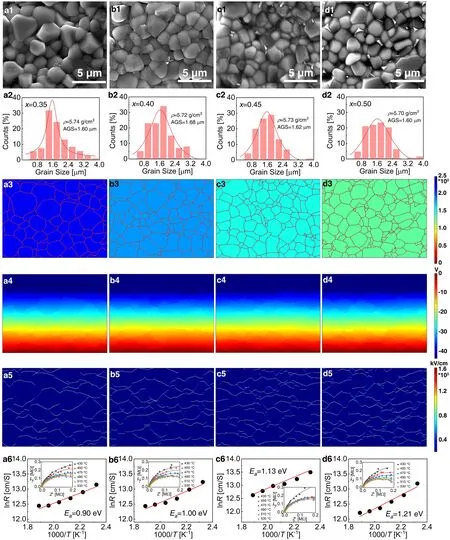
Fig.3 SEM images of surface morphologies for compositions a1 x = 0.35, a2 x = 0.40, a3 x = 0.45, and a4 x = 0.50 ceramics.a2—d2 Grain size distribution.a3—d3 Intensity mapping of εr.a4—d4 Distribution of electric potentials.a5—d5 Local E-field distribution.a6—d6 Relationship between temperature (T) and grain boundary resistance, with resistance spectra shown in the insets
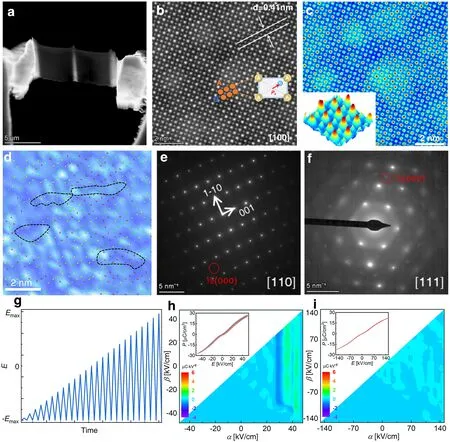
Fig.4 a Bright-field and b high-resolution TEM image of BSB-0.5 ceramic.c Redistribution of brightness based on the RGB values of b.d The polarization vector, calculated from cation displacement on the B-site, superimposed on the polarization intensity distribution, with relative polarization intensity expressed through the brightness and saturation of the background color.SAED patterns along e [110]pc and f [111]pc.g FORC test method.Evolution of FORC distributions for h x = 0.35 and i x = 0.50
Figure 4e and f shows selected area electron diffraction (SAED) patterns along [110]pcand [111]pc, where pc denotes pseudo-cubic.The presence of 1/2(ooo) superlattice points in [110] indicates the R phase, while the presence of 1/2(ooe) superlattice points in [111] indicates the T phase [51].These patterns confirm that the composition withx= 0.50 possesses a phase structure consisting of coexisting R and T phases, consistent with the Rietveld fitting result of XRD.While TEM can reveal domain morphologies at the nanometer scale, it typically provides static results.In contrast, piezoresponse force microscopy (PFM) elucidates polarization switching behavior at the micrometer scale but faces challenges in capturing dynamic details, especially in relaxor ferroelectrics [52].In these materials, PNRs rather than macroscopic domains respond to external driving fields.The switching behavior of individual PNR may vary due to local electric field variations, and historical responses can influence polarization switching behavior.FORC analysis is a valuable technique that can detect a range of residual states dependent on field history.It effectively represents the reaction of local structures in the presence of a uniform electric field and provides a statistical outcome of polarization switches inP-Eloops.This approach incorporates spatial and historical polarization dynamics, offering direct insights into microstructures [53, 54].FORCs ofx= 0.35 and 0.50 ceramics were examined to illustrate macroscopically that in a sample withx= 0.50, all domains are converted into microscopic PNRs.Figure 4g and h—i depicts the principle and FORCs of ceramics withx= 0.35 and 0.50, respectively.In simpler terms, FORC is employed to quantify the number of polarization reversals: A higher value indicates more reversals, while a lower value signifies fewer reversals.The motion of domain barriers is recorded by tracking changes in domains through polarization reversals.In lowE-fields, the low number of ferroelectric phases and the strong nonlinear polarization behavior ofx= 0.35 ceramics at 30 kV cm-1indicate the inversion of ferroelectric domains and the movement of domain walls.This significant hysteresis is a consequence of weak ESP.Even when the sample withx= 0.50 is loaded to 150 kV cm-1, there is no high-intensity distribution, indicating that ferroelectricity is diluted, RFE features are enhanced, and hysteresis is diminished.This is consistent with the exclusive discovery of tiny PNRs by TEM.
3.5 Ferroelectric and ES Performance
Subsequently, the ferroelectric and ES properties of B-xSB ceramic samples were thoroughly assessed.Figure 5a illustrates the unipolarP—Ehysteresis loops of B-xSB samples withx= 0.35, 0.40, 0.45, and 0.50.Owing to the decrease inεr, theEmaxthat can be applied to the sample before electrical breakdown increases with the rising values ofx.For B-xSB samples withxranging from 0.35 to 0.50, the respectiveEmaxvalues are 310, 330, 430, and 460 kV cm-1at a test frequency of 10 Hz.All B-xSB samples exhibited slim hysteresis loops, characteristic of RFE ceramics [9].Asxincreases, theP—Eloops become slimmer.CorrespondingJ—Ecurves are presented in Fig.5b, revealing two distinct current peaks at 50 kV cm-1.The RFE nature of B-xSB samples disrupts long-range ferroelectric order, resulting in the appearance of PNRs.When an appliedE-field is present, PNRs become oriented but are unable to grow into macrodomains and return to random orientation when theE-field drops fromEmaxto zero.Consequently, theJ—Ecurves exhibit twin peaks at lowE-fields.Given the ruled-out AFE nature of BNT-based solid solutions [55, 56], the very slimP—Eloops combined with double current peaks inJ—Ecurves should be described as an AFE-like RFE (AL-RFE) characteristic [8, 57], rather than a relaxor AFE characteristic [58—60].Furthermore, Fig.5b indicates that these two current maxima are roughly symmetric and remain fairly constant asxincreases.It is noteworthy that thePmaxdetermined at the sameEmaxgradually decreases asxincreases from 0.35 to 0.50, owing to the decoupling of A-O and B—O bonds [61].However, the Pmax of B-xSB ceramic samples evaluated at their respectiveEmaxexhibits negligible variation versusx.This suggests that the loss ofPmaxdue to the decoupling effect can be compensated for by increasingEmax.Figure 5a also reveals that thePrhas decreased from 2.64 (x= 0.35) to 0.015 (x= 0.50) μC cm-2, allowing the ΔPandWrecto grow.Wrecandηare determined using the unipolarP—Eloops shown in Fig.5a.When theEmaxincreases by 48% from 310 kV cm-1(x= 0.35) to 460 kV cm-1(x= 0.50), theWrecincreases by 67% from 4.30 J cm-3(x= 0.35) to 7.19 J cm-3(x= 0.50), while theηof B-xSB ceramic samples remains around 90%.This result indicates that thex= 0.50 composition has superior ESP than the other three compositions.Consequently, Fig.5d depicts the comprehensiveP—Eloops and correspondingJ—Ecurves of thex= 0.50 composition measured from 50 to 460 kV cm-1.Under a smallE-field, theJ—Ecurves exhibit a rectangular form.Due to theE-field-induced RFE-to-polar phase transition [27, 56], double current maxima are observed in theJ—Ecurves when theE-field exceeds 150 kV cm-1.The field corresponding to these two maximum values of current scarcely fluctuates, demonstrating that even if theE-field is increased toEmax, the criticalE-field for RFE-to-polar phase transition will remain unchanged.More crucially, as theE-field grows, theP—Eloops remain slim and do not broaden, indicating that no conductive process has been activated, and a highηcan be achieved.Figure 5e depicts theWrecandηof thex= 0.50 composition under variousE-fields.TheWrecgrows monotonously and reaches an impressive value of 7.19 J cm-3at 460 kV cm-1, whereas theηshows very little reduction and still maintains a very high value of 94% at the sameE-field.
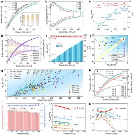
Fig.5 a P—E loops and b the corresponding current density—electric field (J—E) curves for x = 0.35, 0.40, 0.45, and 0.50, measured at RT, 10 Hz, and various E-fields.c Wrec and η of x = 0.35, 0.40, 0.45, and 0.50 ceramics.BDS is indicated next to the data.d P—E loops and corresponding J—E curves for x = 0.50 composition measured at RT and 10 Hz.e Wrec and η of x = 0.50 composition.f Comparison of Wrec and η for BSB-0.50 and other BNT-based bulk ceramics.g Comparison of Wrec for B-0.5SB ceramic with other bulk ceramics.h P—E loops and J—E curves of B-0.5SB ceramic measured at 10 Hz and 366 kV cm-1.Temperature increases from 30 to 140 °C in steps of 10 °C.i Wloss, Wrec, and η calculated from the corresponding P—E loops of B-0.5SB.Temperature-dependent Wrec j and η (k) of B-0.5SB compared with other BNT-based bulk ceramics
Figure 5f compares the ESP of thex= 0.50 ceramic with that of other BNT-based bulk ceramics [25, 62—78].Details regarding the composition,Emax,Wrec, andηof the compared BNT-based bulk ceramics are summarized in Table S3.Clearly, the ESP of thex= 0.50 composition surpasses that of existing BNT-based ceramics.Generally, increasing theE-field improvesWrec.However, in the highE-field region, it appears that augmenting the electric field does not directly enhanceWrec.Although theEmaxvalues of 0.8BNT-0.2Sr(Nb0.5Al0.5)O3[74] and 0.85[0.7BNT—0.3(Bi0.1Sr0.85)TiO3]—0.15KNbO3[72] ceramics are 520 and 569 kV cm-1, respectively, theirWrecvalues are 6.64 and 5.63 J cm-3, which are inferior to theWrecof our ceramic.Conversely, even with highWrecvalues of 7.02 and 6.3 J cm-3at 390 and 420 kV cm-1, theηvalues of 0.78BNT-0.22NaNbO3[65] and 0.85(0.94BNT-0.06BT)-0.15Bi(Mg2/3Nb1/3)O3[25] ceramics, at 85% and 80% respectively, are significantly lower than our ceramic (94%).Consequently, we achieve a comprehensive improvement in ESP with both highWrecand highηin thex= 0.50 ceramic sample.In Fig.5g, the ESP of thex= 0.50 ceramic is compared to that of various representative dielectric ceramic materials, including linear ST-based systems, AFE AgNbO3(AN)-based and NaNbO3(NN)-based systems, and RFE BT-based, KNN-based, BF-based, and BNT-based systems.Details of the composition,Emax,Wrec, andηof the compared systems, are summarized in Table S4.It is evident that linear ST-based systems often have lowWrec(< 4 J cm-3), but AFE AN-based and NN-based systems exhibit higherWrec(4—7 J cm-3) and lowη(50—90%).In contrast, RFE BT-based and KNN-based systems show mediumWrec(2—4 J cm-3) and fluctuatingη(50—95%) under a moderateE-field.Although some BNT-based systems achieve higherWrecand very high η (> 90%), theEmaxhas approached 520—600 kV cm-1.In contrast, ourx= 0.50 composition exhibits highWrec(> 7 J cm-3) and highη(94%) simultaneously at a moderateEmax(460 kV cm-1), indicating a comprehensive improvement in ESP.These findings demonstrate that by manipulatingεr, we were able to create B-xSB ceramics with exceptional ESP in a moderateE-field.As a result, it has emerged as one of the most promising candidate materials for pulse ES ceramic devices.
Temperature stability is a critical criterion for pulse ES ceramic devices [79, 80].The temperature stability of the ESP for thex= 0.50 composition was evaluated using temperature-dependentP—EandJ—Ecurves, as illustrated in Fig.5h.These curves were measured at 365 kV cm-1and 10 Hz, with temperatures ranging from 30 to 140 °C.Typically, in RFEs,PrandEcincrease with rising temperature due to thermal activation of defects, which is detrimental to the stability ofWrecandη[7, 9, 81].As the temperature increases, theP—Eloops remain thin, andPmaxdecreases slightly from 42.7 to 37.0 μC cm-2.The two current peaks indicated by the black arrows show almost no movement with rising temperature.These findings suggest that the ESP in thex= 0.50 composition exhibits good thermal stability.Despite a slight reduction in temperature, theWrecof thex= 0.50 composition decreases from 5.64 J cm-3at 30 °C to 5.06 J cm-3at 140 °C, a 10% reduction, as shown in Fig.5i.Because thePrandEcof thex= 0.50 composition remained reasonably steady, itsηis extraordinarily high, with minimal variations ranging from 93.9 to 95.9%.The temperaturedependent ESP of thex= 0.50 composition is compared to other previously reported BNT-based ceramics in Fig.5j—k [62, 64, 65, 74, 82, 83].The constituents of these BNT-based ceramics are summarized in Table S5 (see Supplementary Information).TheWrecin those BNT-based ceramics typically declines to some extent as temperature rises, with none exceeding 4 J cm-3.In contrast, theWrecof ourx= 0.50 composition is significantly higher than the values of various BNT-based ceramics in the 30—140 °C temperature range, surpassing 5 J cm-3at this temperature range, as shown in Fig.5j.Furthermore, upon comparing theη, it is evident that theηof thex= 0.50 composition remains around 95%.Even with rising temperature, the trend is upward, as illustrated in Fig.5k.In conclusion, in addition to the ultrahigh ESP at RT, the ESP of thex= 0.50 composition demonstrates ultrahighWrecand exceptionalηover a wide temperature range, outperforming other BNT-based ceramics.
3.6 Charge-Discharge Performance
Finally, we evaluate the charge—discharge performance of thex= 0.50 composition, a pivotal criterion for pulse capacitor devices [84].The sample thickness is 100 μm, and the electrode area is 3.14 mm2.Charge—discharge tests employ a 100-Ω resistor.A dielectric ceramic with rapid charge/discharge characteristics is well-suited for pulse power supply.Room temperature electric current versus time (I—t) curves measured in an overdamped discharge mode are presented in Fig.6a.TheImaxincreases with the escalating electric field.Wdisattains its peak value of 3.89 J cm-3under 400 kV cm-1, as depicted in Fig.6b.The time at whichWdisreleases 90% of its total energy, often denoted ast0.9, is crucial for calculating discharge speed.At 100 kV cm-1, thet0.9for thex= 0.50 composition is approximately 0.21 μs, diminishing with increasing electric field.At 400 kV cm-1,t0.9is less than 0.12 μs.Figure 6c illustrates the temperaturedependentI—tcurves from 40 to 140 °C, determined at overdamped discharge mode under anE-field of 300 kV cm-1.Thet0.9remains below 0.13 μs at all measured temperatures, as demonstrated in Fig.6d.TheI—tcurves of underdamped discharge at differentE-fields are presented in Fig.6e, and the calculated current density (CD) and power density (PD) are displayed in Fig.6f.The discharge of thex= 0.50 composition is confirmed to be complete after only two oscillations.At 400 kV cm-1,CDandPDare exceedingly high at 767.5 A cm-2and 153.5 MW cm-3, respectively.These features indicate that thex= 0.50 composition ceramics exhibit significant potential for use in pulse power devices [7, 82].

Fig.6 Pulsed overdamped discharging properties of B-0.5SB bulk ceramics, illustrating a current curves and b Wdis at RT and various electric fields.Temperature-dependent pulsed overdamped discharging properties of B-0.5SB bulk ceramics, depicting c current curves and d Wdis at 300 kV cm-1 as the temperature increases from 40 to 140 °C in intervals of 20 °C.Pulsed underdamped discharging properties of B-0.5SB bulk ceramics, exhibiting e current curves, and f CD and PD as functions of the electric field at RT
4 Conclusions
In summary, we propose an approach to achieve optimal ESP under constrainedE-field conditions by tailoring theεr.Ultimately, thex= 0.50 composition demonstrates an extraordinaryηof 93.8% and an impressiveWrecof 7.19 J cm-3at a moderateE-field.The temperature-dependent ESP of thex= 0.50 composition is also notably robust.Across the temperature range of 30—140 °C,Wrecconsistently exceeds 5 J cm-3with high efficiency (above 95%).In contrast with other BNT-based bulk ceramic capacitors, the B-0.5SB ceramic, with its exceptional ESP, undoubtedly stands out as a promising candidate for future ES devices.Moreover, the B-0.5SB ceramic exhibits an ultrahigh current density and power density, simulating real-world application scenarios.Although this study employed linear dielectrics as a model and acknowledges some discrepancies between research results and theoretical conclusions, it addresses a crucial research gap concerning the attainment of high ESP in a restrictedE-field.To conclude, this strategy, involving the modification ofεr, enhancement of insulating properties, and incorporation of domain engineering, proves effective.It is anticipated that these findings will contribute to and guide future research and development endeavors in the realm of ceramic capacitors.
AcknowledgementsThis work was supported by the National Natural Science Foundation of China (Grant No.51761145024), the Key Research and Development Program of Shaanxi (Program No.2022KWZ-22), the Natural Science Basic Research Program of Shaanxi (Program No.2023-JC-YB-441), the Youth Innovation Team of Shaanxi Universities, and the Fundamental Research Funds of Shaanxi Key Laboratory of Artificially-Structured Functional Materials and Devices (AFMD-KFJJ-21203).The research was made possible by Russian Science Foundation (Project No.23-42-00116).The equipment of the Ural Center for Shared Use “Modern nanotechnology” Ural Federal University (Reg.No.2968) which is supported by the Ministry of Science and Higher Education RF (Project No.075-15-2021-677) was used.The SEM work was done at International Center for Dielectric Research (ICDR), Xi’an Jiaotong University, Xi’an, China.The authors also thank Shiyanjia Lab (www.shiya njia.com/ paper award.html) for providing assistance with TEM characterization.
Declarations
Conflict of interestThe authors declare no interest conflict.They have no known competing financial interests or personal relationships that could have appeared to influence the work reported in this paper.
Open AccessThis article is licenced under a Creative Commons Attribution 4.0 International License, which permits use, sharing, adaptation, distribution, and reproduction in any medium or format, as long as you give appropriate credit to the original author(s) and the source, provide a link to the Creative Commons licence, and indicate if changes were made.The images or other third-party material in this article are included in the article’s Creative Commons licence, unless indicated otherwise in a credit line to the material.If material is not included in the article’s Creative Commons licence and your intended use is not permitted by statutory regulation or exceeds the permitted use, you will need to obtain permission directly from the copyright holder.To view a copy of this licence, visit http:// creat iveco mmons.org/ licen ses/ by/4.0/.
Supplementary InformationThe online version contains supplementary material available at https:// doi.org/ 10.1007/ s40820- 023- 01290-4.

- Nano-Micro Letters的其它文章
- A Generic Strategy to Create Mechanically Interlocked Nanocomposite/Hydrogel Hybrid Electrodes for Epidermal Electronics
- Atomically Substitutional Engineering of Transition Metal Dichalcogenide Layers for Enhancing Tailored Properties and Superior Applications
- Chalcogenide Ovonic Threshold Switching Selector
- Highly Efficient Aligned Ion-Conducting Network and Interface Chemistries for Depolarized All-Solid-State Lithium Metal Batteries
- Integrating Levels of Hierarchical Organization in Porous Organic Molecular Materials
- Enhancing Green Ammonia Electrosynthesis Through Tuning Sn Vacancies in Sn-Based MXene/MAX Hybrids