
Modulated optical and ferroelectric properties in a lateral structured ferroelectric/semiconductor van der Waals heterojunction
2023-12-15 11:48ShanshanChen陈珊珊XinhaoZhang张新昊GuangcanWang王广灿ShuoChen陈朔HeqiMa马和奇TianyuSun孙天瑜BaoyuanMan满宝元andChengYang杨诚
Chinese Physics B 2023年12期
Shanshan Chen(陈珊珊), Xinhao Zhang(张新昊), Guangcan Wang(王广灿), Shuo Chen(陈朔),Heqi Ma(马和奇), Tianyu Sun(孙天瑜), Baoyuan Man(满宝元),2,‡, and Cheng Yang(杨诚),2,3,†
1School of Physics and Electronics,Shandong Normal University,Jinan 250014,China
2Institute of Materials and Clean Energy,Shandong Normal University,Jinan 250014,China
3Shandong Provincial Engineering and Technical Center of Light Manipulations,Shandong Normal University,Jinan 250014,China
Keywords: ferroelectric tunnelling junction, metal/ferroelectric/semiconductor, tunnelling electroresistance,optoelectronic properties
1.Introduction
Memristors are ideal building blocks for brain-like neuromorphic devices.[1-6]A two-terminal structured ferroelectric tunnelling junction(FTJ)has transmission properties similar to the biological synapse; its top and bottom electrodes are commonly used to mimic the presynaptic and postsynaptic membranes in biological synapses.[7]Traditional memristors that achieve basic synaptic functions by applying voltage alone are purely electronic synapses; however, they lack the function of mimicking sensory cells in a biological nervous system.
Some researchers have introduced light stimulation to mimic functions in sensory cells.[7-10]Shenet al.reported TiNxO2-x/MoS2/indium tin oxide (ITO) devices that showed basic analog resistive switching behavior and various basic synaptic functions such as short-term plasticity and long-term plasticity,and finally constructed a 4×4 photoelectric synapse array that was used to simulate human visual perception and visual memory functions.[7]To achieve light stimulation,most artificial optoelectronic synapses are typically designed as vertical structures with transparent ITO as the top electrode.However, it is challenging to fabricate thin ITO films; the transmittance of ITO is generally<90%and it decreases with increase in film thickness.[8]Lateral structured devices fabricated using a thin two-dimensional(2D)material can be used to realize the role of light-stimulated synapses.
Two-dimensional(2D)ferroelectric CuInP2S6(CIPS)has shown excellent ferroelectric properties;[11-13]it can be used to switch polarization in flakes down to several layers at room temperature,[11]and it can be easily integrated onto flat substrates to form FTJ devices due to their strong intralayer coupling and weak interlayer interactions.[13]Recently, Sun and colleagues showed that a tunnelling electroresistance(TER)of over 107could be obtained by using a thin CuInP2S6/graphene junction.[12]Further research could help realize sensory devices using CIPS as a ferroelectric material.
As a 2D semiconductor material,MoS2has a strong and fast photoresponse[14,15]that benefits the integration of fieldeffect transistors into other new sensing devices.Furthermore,van der Waals (vdW) heterojunctions based on MoS2and other materials, including MoS2/Si,[16]MoS2/WSe2[17]and MoS2/h-BN/graphene,[18]are widely used in optoelectronic applications.Based on the advantages of MoS2,combining it with CIPS to construct a lateral structured Au/CIPS/MoS2/Au vdW heterojunction could possibly realize sensory devices with 2D vdW junctions.
Semiconductors are also crucial for forming a Schottky barrier to obtain a higher TER, which is essential for the FTJ.[19-24]For vertical structured FTJ devices, an enhanced TER(∼103-104)can be obtained using the ferroelectric/semiconductor heterojunction.[22-24]To the best of our knowledge, no lateral structured ferroelectric/semiconductor FTJ with a higher TER(>104)has been reported.
2.Results and discussion
We demonstrated that lateral structured Au/CIPS/MoS2/Au vdW heterojunctions could be used in planar FTJ devices,combining excellent TER and optical properties.Figure 1(a)shows a schematic diagram of a lateral structured device.Ferroelectric CIPS flakes were used as the ferroelectric material to realize polarized ON and OFF states.Semiconductor MoS2flakes were used to modulate the barrier height and width of the memristors and as the optoelectronic material of the photodetector.Both CIPS and MoS2flakes were transferred onto a patterned high-work-function Au electrode;details are presented in the supporting information section‘Device fabrication’.Devices with different ferroelectric mechanisms andI-Vcharacteristics are shown in Fig.1.
The formation mechanisms of the ON and OFF states of the proposed CIPS/MoS2heterojunction were analyzed and are shown in Fig.1(b).The work function of Au is 5.1 eV,[25]the electron affinity of CIPS is 3.7 eV and the indirect band gap of MoS2is 1.365 eV.[12,26]When different voltages were applied to the device,the polarization directions of CIPS were different, resulting in two different resistance states.The polarization direction of CIPS pointed to MoS2when a positive polarization voltage was applied, which generated pairs of bound polarized charges in the dielectric CIPS flakes (left of Fig.1(b)).The positive bound polarized charges attracted electrons in MoS2, causing the accumulation of electrons at the MoS2surface of the CIPS-MoS2interface.Thus, the depletion region of MoS2was annihilated.The conductivity of MoS2also improved when electrons gathered at the MoS2surface to fill the conduction band of MoS2.In this case,MoS2flakes were the n+-type semiconductor that formed the metal/ferroelectric/semiconductor-type FTJ.[24,27,28]A depolarization field,opposite to the polarization direction,was easily formed in the CIPS ferroelectric barrier and benefited from the incomplete screening of the MoS2films.Such a depolarization field lowers the Schottky barrier height (SBH) and generates a higher tunnelling transmittance,inducing a larger tunnelling current.[29]Therefore, the decreased barrier height at the CIPS-MoS2interface resulted in a low resistance (ON state).
In contrast,the CIPS polarization direction deviated from the MoS2flakes when a negative polarization voltage was applied (right side of Fig.1(b)).Negative bound polarized charges caused the depletion of electrons at the MoS2side of the CIPS-MoS2interface.The width of the depletion region(i.e.,the effective barrier width)increased due to electron depletion at the interface,[20]and the accumulation of holes at the CIPS-MoS2interface decreased the conductivity of MoS2.The immobile ionized donors at the MoS2surface screened the negative bound polarized charges at the CIPS surface.Such screening is usually insufficient[24,27,28]to produce a depolarization field and increases the SBH at the CIPS-MoS2interface.The increased barrier width and height provide greater resistance to stop the tunnelling current through the heterojunction,resulting in a device with high resistance(OFF state).The realization of ON and OFF states can be mainly attributed to the modulation of the SBH and width by the CIPS polarization reversal and the screening of the MoS2flakes.
Semiconductor MoS2is crucial for modulating the barrier width and height to improve TER.To analyze the effect of the semiconductor MoS2,an Au/CIPS/Au FTJ without MoS2flakes was also fabricated (Fig.1(d)).The formation mechanisms of the ON and OFF states are analyzed in Fig.1(e).The top Au electrode(work function=5.24 eV)[30]was prepared using the transfer method (details in the supporting information section‘Au electrode fabrication,release,transferring and lamination process’),and the bottom Au electrode(work function=5.1 eV)[25]was customized using photolithography to realize the asymmetry of the electrodes.At different voltages,the electric field-induced CIPS polarization changed the band alignment of CIPS at the Au-CIPS interface,resulting in two resistance states(ON and OFF states).When the polarization direction of CIPS is upward,negatively polarized charges are generated at the bottom of the CIPS and positively polarized charges accumulate on the top of the CIPS.The ferroelectric polarized charges cannot be fully compensated by the electrode charges due to interfacial effects.[31]The built-in internal field is directed from the positive to the negative polarized charges, causing the SBH to be reduced.[29,31]The device is in a low-resistance state(ON state).When the polarization direction of CIPS is downward,the CIPS generates the opposite polarized charges and the polarization reversal of CIPS alters the built-in internal field,which increases the SBH.[29,31]The device is in a high-resistance state(OFF state).Such vertical structured Au/CIPS/Au only modulated the barrier height to improve TER.
TER is considerably influenced by the width and height of the potential barrier;[29]the equation for TER is given by[32]
Under the Wentzel-Kramers-Brillouin (WKB) approximation,the current density is given by[33]
whereCandα(V)are expressed asC=-(4em)/(9π2¯h3)andα(V)=[4d(2m)1/2]/[3¯h(ϕ1+eV-ϕ2)].If the difference between potential steps ∆ϕ ≡ϕ2-ϕ1is too small compared with the average potential barrier, ¯ϕ ≡(ϕ2+ϕ1)/2,then ∆ϕ/2< ¯ϕ.In the case of a small bias voltage,Eq.(2)can be approximated as[32]
Therefore, TER increases with the barrier heightδϕ, as expressed in Eq.(4).The change in the barrier height of the CIPS-MoS2interface is much larger than that of the CIPS-Au interface when the barrier height of the CIPS-MoS2interface is modulated,which increases TER.
Obviously,TER increases with an increase in the barrier width of the depletion regiond, as calculated using Eq.(4).The barrier width of the depletion region is related to the effective free carrier concentration of the semiconductor.The relationship between the width of the depletion region and the effective free carrier concentration is shown below:[34]
whereεsis the dielectric constant of semiconductors,Vbiis the built-in potential andNeffis the effective free carrier concentration.
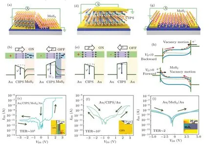
Fig.1.(a)Schematic diagram of a lateral structured Au/CIPS/MoS2/Au vdW FTJ.(b)Band diagrams for the ON and OFF states of the Au/CIPS/MoS2/Au vdW FTJ.(c)I-V curve of the Au/CIPS/MoS2/Au vdW FTJ with clear switching behavior and low operation voltage.(d)Schematic diagram of a vertical structured Au/CIPS/Au FTJ.(e)Band diagrams for the ON and OFF states of the Au/CIPS/Au FTJ.(f)I-V curve of the Au/CIPS/Au vdW FTJ with switching behavior.(g) Schematic diagram of a lateral structured Au/MoS2/Au.(h) Band diagrams at different bias voltages of the lateral structured Au/MoS2/Au.The green curve above represents the conduction band before the voltage sweep and the red dotted line represents the change in the Schottky barrier height.(i)I-V characteristics of the Au/MoS2/Au junction in both forward and backward states;the inset is an optical image of the device.
For the case of n+-type MoS2, the effective free carrier concentration decreases at high resistance (OFF state),which can be attributed to the depletion of electrons at the MoS2surface, increasing the width of the depletion region.However, for the Au/CIPS/Au device, it is difficult to change the barrier width at the CIPS-Au interface.Therefore,the change in the barrier width shows that the TER of the Au/CIPS/MoS2/Au vdW FTJ is higher than that of the Au/CIPS/Au FTJ.Thus, the analysis of the effects of barrier height and width on the improvement of TER suggested that an Au/CIPS/MoS2/Au vdW FTJ can significantly improve TER.
ExperimentalI-Vhysteresis loops of Au/CIPS/MoS2/Au and Au/CIPS/Au junctions are shown in Figs.1(c) and 1(f).The asymmetric hysteresis of the Au/CIPS/MoS2/Au FTJ may be attributed to the asymmetric contact.[35]I-Vcharacteristics of the devices in the voltage range from 3 to-3 V are shown in Fig.S2.In the OFF state, the tunnelling current of the proposed Au/CIPS/MoS2/Au FTJ is one order of magnitude smaller than that of the Au/CIPS/Au FTJ.In the ON state,the tunnelling current of the proposed Au/CIPS/MoS2/Au FTJ is two orders of magnitude larger than that of the Au/CIPS/Au FTJ.Thus, introducing MoS2to the construction of lateral structured Au/CIPS/MoS2/Au vdW FTJ devices significantly improves the TER(by three orders of magnitude).A TER of∼1.4×10⁴was obtained for the proposed lateral structured Au/CIPS/MoS2/Au vdW FTJ devices.
The ferroelectric properties of CIPS are crucial.The Au/MoS2/Au junction without the CIPS flakes[Fig.1(g)]resembles only a Schottky diode.[36]The inhibitory behavior of the MoS2-Au potential barrier for improving TER is almost negligible.The modulation of the MoS2/Au SBH can be qualitatively described by the band diagrams shown in Fig.1(h).According to Liet al., the switching behavior of resistance states is mainly attributed to the redistribution of sulfur(S)vacancies under the electric field.[37]The influence of impurity movement on the interface between MoS2and the substrate,and the adsorption of charged impurities by MoS2in the environment, are ignored.Under negative bias (backward), S vacancies drift from the left to the right electrode.[37]This decreases and increases the density of S vacancies at the left and right electrodes, respectively.As a result, the SBH on the left and right sides decreases and increases, respectively.Conversely, under positive bias (forward), S vacancies drift from the right to the left electrode.TheirI-Vcharacteristics are shown in Fig.1(i).TheIforward/Ibackwardratio is extremely small under both positive and negative biases.The defects of S vacancies drift under voltage bias,and any further influence of barrier height and width in the Au/CIPS/MoS2/Au devices is almost negligible.Thus, data retention can be attributed to the polarization-induced ON-OFF states.
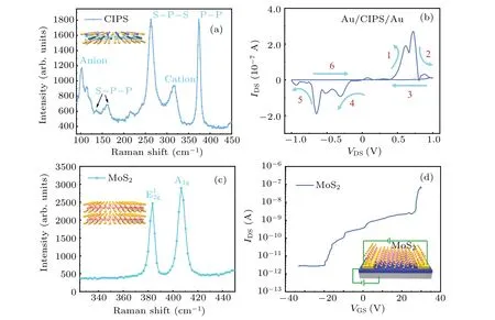
Fig.2.(a)Raman spectra of CIPS flakes measured at room temperature.(b)I-V characteristics of CIPS flakes.(c)Raman spectra of MoS2 flakes measured at room temperature.(d)IDS-VG characteristics of the MoS2 transistors.
The CIPS and MoS2materials were characterized using Raman andI-Vcharacteristic curve tests.Figure 2(a) shows the Raman spectra of the CIPS flakes at room temperature.Because of the anion (P2S4-6 ) liberation, a peak at 102 cm-1is easily observed.The presence ofδ(S-P-P) andδ(S-PS) modes leads to multiple Raman peaks of 140-290 cm-1.The presence of the cations (CuI, InIII) leads to the appearance of a Raman peak at 316.5 cm-1.Theν(P-P)mode results in a peak at 373.7 cm-1.[38]Figure 2(b) shows theI-Vcharacteristics of the CIPS flakes.TheI-Vcurves were divided into six parts at 0 V→1 V→0 V and 0 V→-1 V→0 V, with multiple peaks appearing in the sweep voltage.The two-step 90◦switch polarization reversal was responsible for these peaks,demonstrating the ferroelectric nature of CIPS flakes.[39]Figure 2(c) shows the Raman spectra of the MoS2flakes.The out-of-plane (E12g) and in-plane resonance peaks(A1g)of MoS2can be observed at 383.5 cm-1and 406.6 cm-1,respectively.[40]The distance between the two characteristic peaks is approximately 23.1 cm-1.Referring to the previous data, this difference of approximately 23.1 cm-1represents four layers of MoS2flakes.[41,42]Figure 2(d)tests theIDS-VGcharacteristics of the MoS2transistors.The transmission characteristics show typical n-type semiconductor characteristics under a sweep gate voltage from-33 V to 33 V.[43,44]
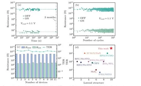
Fig.3.(a)Data retention characteristics of the device in the ON and OFF states.(b)Endurance characteristics of the device.Experimental measurements were obtained for 1000 switching cycles.(c)Resistances(ON and OFF states)of the 11 different FTJ devices and the corresponding TERs.(d)TERs of the reported lateral structured devices.
Our proposed Au/CIPS/MoS2/Au vdW FTJs with 11 nm CIPS and 2 nm MoS2(figure S3 shows material thickness)exhibited good reliability, such as long data retention, excellent endurance performance and uniformity.The electrical characteristics and properties were tested and analyzed and are shown in Fig.3.Figure 3(a) shows the data retention properties at room temperature.The TER was stable at 1.4×10⁴after more than 2 months, which showed that the proposed device has a robust performance.[12,45]Figure 3(b)shows the endurance test of the FTJ over 1000 cycles.After 1000 cycles,the TER remained above 1.4×10⁴,indicating good endurance of the device.Several devices were prepared and tested for different values of resistance and TER in the ON and OFF states, as shown in Fig.3(c).The device exhibited good uniformity.The TER of the proposed vdW FTJ compared with that of the other lateral structured devices[46-54]is shown in Fig.3(d).Our proposed vdW FTJ showed the highest TER for the lateral structured devices.The Au/CIPS/MoS2/Au vdW FTJ demonstrated non-volatile switching and non-destructive readout reliability and is thus considered an ideal candidate for high-TER memory.[55]
The direct tunneling and Fowler-Nordheim tunnelling(FNT)mechanisms are the main transport mechanisms in our proposed Au/CIPS/MoS2/Au vdW FTJ.There are three main possible transport mechanisms: direct tunnelling, FNT and thermionic emission.[56]The physical phenomenon of FNT is the same as that of direct tunnelling; however, at different voltage states, FNT tunnelling occurs at higher voltages.[24]To prove that the tunnelling mechanism of carriers is also independent of thermal emission, theI-Vcharacteristics of the proposed Au/CIPS/MoS2/Au vdW FTJ at different temperatures and the corresponding TER were obtained and are shown in Fig.S4.The current exhibited a weak change in the temperature range 250-340 K for the ON and OFF states,and the TER remained almost the same.According to the current density formula for the thermionic emission[57,58]
the thermal activation process of the thermionic emission mechanism led to strong temperature dependence(J∝T).The unchanged TER shows that the transport mechanism is independent of the thermionic emission.TheI-Vcharacteristic curve of the device under different voltages was fitted as shown in Fig.S5.It is known that if ln(I/V2)∝1/Vis satisfied FNT prevails,[59]and if ln(I/V2)∝ln(1/V)is satisfied direct tunnelling plays a leading role.Both FNT and direct tunnelling can be observed in the fitting results.[60]By fitting the experimental data, it can be found that the primary tunnelling mechanism is direct tunneling under low voltage.As the voltage increases,FNT becomes dominant.
The proposed Au/CIPS/MoS2/Au vdW FTJ also exhibited excellent photoresponsive properties, benefiting from the light absorption properties of the MoS2semiconductor.The Au/CIPS/MoS2/Au vdW FTJ had a rather low current when the polarization direction of CIPS was downward(OFF state) (Fig.1(c)).A low dark current has been found to be critical for high-performance photodetectors.To elaborate the performance mechanism when the device was laserilluminated (449 nm laser), the energy band arrangements of the CIPS/MoS2heterojunction under different polarization states are shown in Fig.4(a); the inset of Fig.4(a) shows a schematic diagram of the device.The photogenerated electrons and holes are easily separated and collected to form photocurrents.When the polarization direction of CIPS is upward(ON state),the bending of the MoS2energy band at the interface changes from bottom to top.Due to the positive polarized charges accumulating at the interface, free electrons are attracted and free holes are repelled opposite to the current direction.The dark current is also larger, because of which the change in the photocurrent is insignificant in the ON state.When the polarization direction of CIPS is downward (OFF state), the energy band remains upward.Free electrons are repelled,and free holes are attracted due to the negatively polarized charges accumulating at the interface,the same as the current direction.At this time, the dark current is small, and the photocurrent easily increases under illumination.Therefore, the photocurrent can be mainly attributed to the contribution of photogenerated electrons under positive bias and the dark current is smaller,which improves the photoresponse behavior.
Figure 4(b)shows the hysteresis loops(VDSwas between-4 V and 4 V) of the generated photocurrents with different polarization states under 449 nm laser irradiation.Figure 4(c) shows the dependence of photocurrent as a function of light intensity (VDS= 1.3 V).In the ON state, the magnitude of the current is almost constant.However, the photocurrent of this device in the OFF state strongly depends on the light intensity and increases with increase in light intensity.In the OFF state,the current of the device increases from 4×10-12A to 1.2×10⁻¹⁰A when light intensity increases from 0 to 0.57 mW·cm-2; the value ofIlight/Idarkis 30.A better linear relationship is obtained, demonstrating that the device has excellent photoresponsive performance in the OFF state.
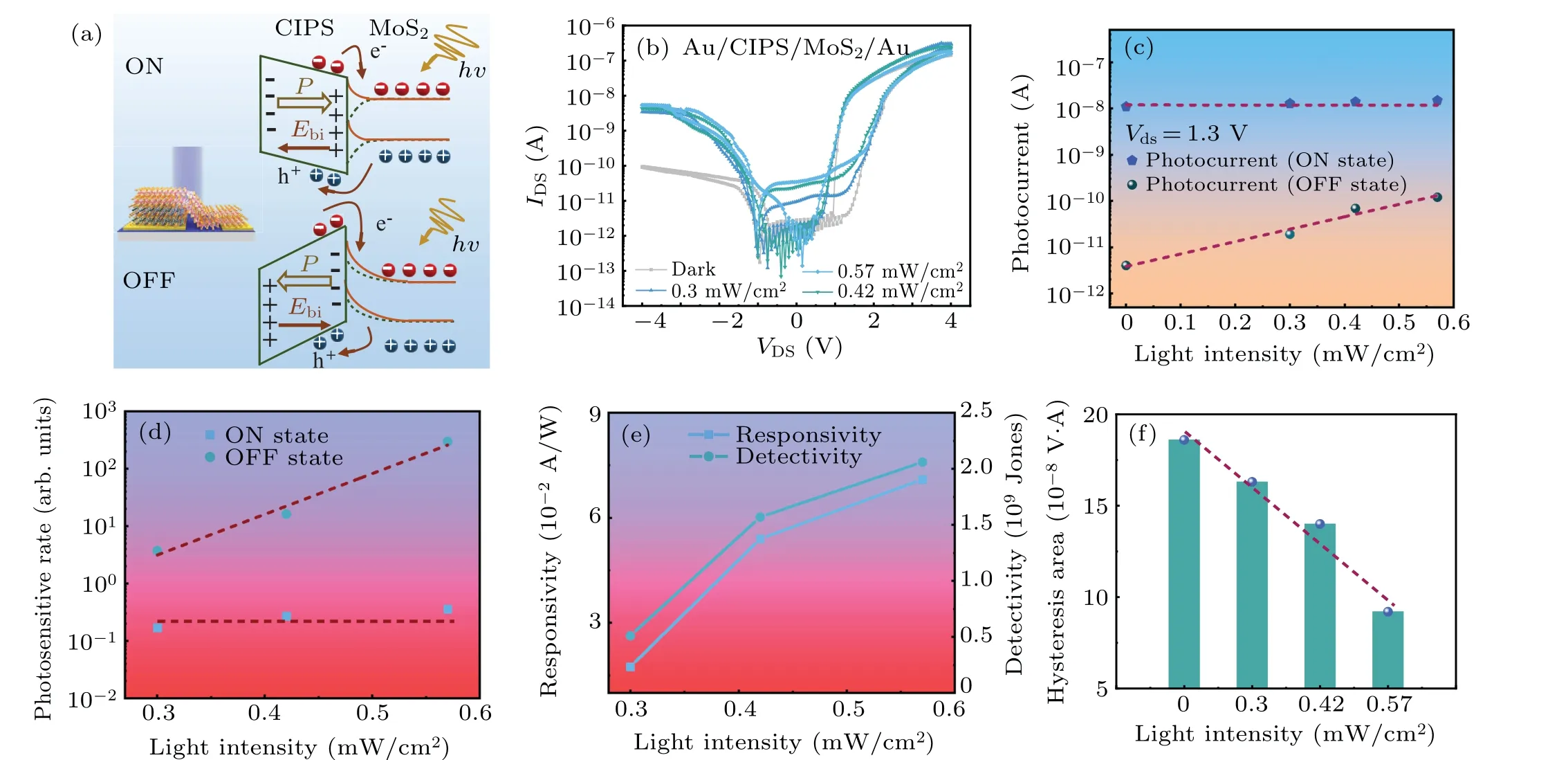
Fig.4.(a) Band diagrams of the photodetector in the ON and OFF states; at VDS =1.3 V, the green dotted line is the energy band without light and the 0 V bias voltage,and the solid orange line is the energy band at 1.3 V bias voltage with a 449 nm laser.(b)Hysteresis loops under different light intensities for a 449 nm laser.(c) Photocurrent as a function of light intensity in the ON and OFF states.(d) Photosensitive rate as a function of the light intensity of the device in the ON and OFF states.(e)Responsivity and detectivity of the proposed Au/CIPS/MoS2/Au vdW FTJ photodetector as a function of light intensity in the OFF state.(f)Hysteresis loop area as a function of light intensity.
The difference in the dark currents in the ON and OFF states is the main reason for the difference in the photoresponsive performance in the ON and OFF states.The dark current in the ON state is much higher than that in the OFF state.Light stimulation onto the device in the ON state cannot easily increase the current, because the dark current in the ON state is already very high.Light stimulation onto the device in the OFF state easily increases the current, benefiting from the very slow dark current in the OFF state.A new parameter of the photosensitive rate(Rp)as a function of the light intensity is proposed here to analyze the effects of the ON and OFF states;the relationship is defined using
whereIlightis the light current andIdarkis the dark current.As shown in Fig.4(d),the photosensitive rate in the OFF state to the light stimulation is much greater than that in the ON state.
Photoresponsivity (Rλ) and detectivity (D∗), which are important parameters for evaluating the ability to convert light signals into electrical signals,[61]were analyzed in the OFF state and are shown in Fig.4(e).RλandD∗can be calculated as defined in Ref.[62]
wherePis the light power,Ais the photosensitive area andeis the electron charge.Values ofRλ=7.1×10⁻²A·W-1andD∗=2.06×10⁹Jones were obtained in the OFF state.Our experiment shows excellent detector sensitivity in the OFF state.
Light stimulation can be used to modulate the ferroelectric properties,and the ferroelectric properties can yield a new type of photodetector with the new parameters.The new parameter of the hysteresis loop area as a function of light intensity was analyzed to obtain the relationship between the ferroelectric and photodetection properties, as shown in Fig.4(f).The linear relationship provides a new characteristic for analyzing the photodetector.
The modulated relationship between ferroelectric TER and photosensitive rateRpcan be summarized by
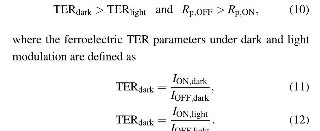
The photosensitive rates(Rp)in the different ferroelectric ON and OFF states are defined as
It should be mentioned that a larger TERdarkis the key point for obtaining two types of photodetection properties in a device.For our proposed ferroelectric CIPS/semiconductor MoS2-based heterojunction,if TERdarkis already large enough(∼104),the dark current in the ON state(∼10-8A)is already comparable to or of the same order as the current of the MoS2junction under light irradiation and the photoresponsive performance in the ON state is weak.
Schematic diagrams of the ferroelectric TER parameter in the ferroelectric/semiconductor heterojunction and the photoelectricIlight/darkparameter in the semiconductor junction are shown in Fig.5.When the TERON/OFFis the same order asIlight/dark, the photoresponsive performance in the ON state is negligible.Two types of photodetection properties in one device can be obtained.
Fig.5.Schematic diagrams of the ferroelectric TER and the photoelectric Ilight/dark parameter in the ferroelectric/semiconductor heterojunction and semiconductor junction.
3.Conclusion
A combination of higher TER and excellent optoelectronic properties can be obtained by using a lateral structured Au/CIPS/MoS2/Au vdW FTJ.CIPS polarization directions are easily modulated by an applied voltage to form the ON and OFF states.The barrier width and height at the CIPSMoS2interface were modulated to improve the TER.The ferroelectric and photodetection properties modulated each other.The results show that the devices composed of 2D ferroelectric materials and 2D semiconductors exhibit excellent nonvolatile and photoresponsive performance,providing an excellent method for developing high-TER memristors or preparing new photodetectors.
Acknowledgement
Project supported by the National Natural Science Foundation of China(Grant Nos.11874244 and 11974222).

- Chinese Physics B的其它文章
- Diamond growth in a high temperature and high pressure Fe-Ni-C-Si system: Effect of synthesis pressure
- Multi-channel generation of vortex beams with controllable polarization states and orbital angular momentum
- Calibration of quantitative rescattering model for simulating vortex high-order harmonic generation driven by Laguerre-Gaussian beam with nonzero orbital angular momentum
- Materials and device engineering to achieve high-performance quantum dots light emitting diodes for display applications
- From breather solutions to lump solutions:A construction method for the Zakharov equation
- Complete population transfer between next-adjacent energy levels of a transmon qudit