
Wet flashover voltage improvement of the ceramics with dielectric barrier discharge
2023-11-19 13:32:18ChengshuoHUANG黄成硕XiangqianXIE解向前YangyangZHOU周洋洋XiZHU祝曦XingleiCUI崔行磊andZhiFANG方志
Plasma Science and Technology 2023年11期
Chengshuo HUANG(黄成硕) ,Xiangqian XIE(解向前) ,Yangyang ZHOU(周洋洋) ,Xi ZHU(祝曦) ,Xinglei CUI(崔行磊),* and Zhi FANG(方志)
1 Nanjing Tech University College of Electrical Engineering and Control Science,Nanjing 211816,People’s Republic of China
2 Zhongtian Technology Industrial Wire and Cable System Co.Ltd.,Nantong 226010,People’s Republic of China
Abstract Surface modification techniques with plasma are widely investigated to improve the surface insulation capability of polymers under dry conditions,while the relationship between treatment method,surface physical and chemical properties,and wet flashover voltage is still unclear for inorganic ceramics.In this work,the surface insulation properties of ceramics under wet conditions are improved using nanosecond-pulsed dielectric barrier discharge with polydimethylsiloxane(PDMS)as the precursor.The relationships between PDMS concentration and the water contact angle,dry and wet flashover voltages are obtained to acquire the optimal concentration.The surface charge dissipation test and surface physio-chemical property measurement with SEM,AFM,XPS are carried out to further explore the mechanism of surface insulation enhancement.The results show that film deposition with micron thickness and superhydrophobicity occurs at the PDMS concentration of 1.5%.The dry flashover voltage is increased by 14.6% due to the induction of deep traps,while the wet flashover voltage is increased by 66.7%.The gap between dry-wet flashover voltage is decreased by 62.3% compared with the untreated one due to the self-cleaning effect.
Keywords: dielectric barrier discharge,insulating ceramic,wet flashover,film deposition
1.Introduction
Ceramic materials have become an indispensable insulating material because of their high mechanical strength,wear resistance,excellent insulation properties at high temperatures and high frequencies.In recent years,the rapid development of new energies places significant demands for high-voltage power modules with a smaller package and higher operating voltage,which brings severe challenges to packaging insulation[1].The ceramic is widely used for high-voltage power module packaging insulation in power electronic industries [2].However,their long-term exposure to environments with a high content of humidity such as seaward wind power station is prone to flashover due to high hydrophilicity,seriously constricting their applications[3].Worse still,the wet flashover voltage is lower than the dry flashover one resulting in more hazards [4,5].As the wet flashover voltage is dependent on surface physio-chemical properties,various methods have been explored for surface modification,such as physical polishing,direct fluorination,and low-temperature plasma material surface treatment[6-8].Plasma surface modification is highly controllable by adding different types and number of precursors in the discharge region to produce desirable surface physicochemical properties[9-11].At present,dielectric barrier discharge(DBD)under atmospheric pressure is one of the most widely used plasma source for surface modification,which is easy to realize continuous treatment and has a broad prospect in large-scale industrial applications.
Atmospheric pressure DBD has been demonstrated to be an effective approach to improve surface flashover voltage.Shao et al increased the roughness of the PMMA surface and introduced fluorine elements from the CF4reaction medium to enhance surface electro-trapping ability,resulting in a 69.8% increase in the vacuum flashover voltage [12].Wang et al deposited a nanometer-thick silicon oxide (SiOx) film on the epoxy resin surface to control surface charge,resulting in a 42% increase in its flashover voltage[13].Xie et al deposited a SiCxHyOzthin film on the epoxy resin surface to introduce shallow traps and enhance the flashover voltage[7].It can be summarized from current studies that DBD treatment can change the physical morphology and chemical composition of the material surface by etching,implementing functional groups,and film deposition to shallow the trap level for accelerating surface charge dissipation and improving the flashover voltage.However,most of the relevant research revolves around the modification of polymers under dry conditions,while little is known on the method of improving the wet flashover of ceramic materials.
The surface modification effect varies significantly for diverse materials with different treatment methods and conditions [14-16].Ceramics as inorganic materials possess crystalline granular structures with special physical morphology and chemical bonding compared to polymers.Therefore,the physicochemical process of plasma interaction with ceramic surfaces and the modification effect are different from those of polymers.In addition,most studies investigated the flashover voltage in a dry environment without considering the wet flashover problem [17].Plasma treatment conditions and optimal effects for improving the wet flashover voltage of ceramic materials are poorly understood,and the associated relationships between plasma treatment conditions,ceramic surface physical and chemical properties,and wet flashover voltage are still obscure.It is necessary to carry out research on plasma treatment methods and mechanisms for the improvement of the wet flashover voltage of ceramics.
In this work,a nanosecond-pulse excited DBD is employed for the treatment of the ceramics to improve their wet flashover voltages.Polydimethylsiloxane (PDMS) is chosen as the precursor,as it is the most widely used reagent in industrial applications for the deposition of siloxane-like films due to its chemical inertness,low toxicity,and high saturation vapor pressure.The nanosecond pulse power supply is used for its strong reduced electric field,with large initial electron density and high electron energy,which promote the fragmentation and polymerization of the precursor [18-20].The surface treatment of ceramic materials is performed by adding different concentrations of PDMS to obtain optimal condition.The water contact angle (WCA),dry and wet flashover voltage,and charge dissipation rate variations are measured.To further investigate the mechanism of ceramic wet flashover voltage enhancement,the surface physical and chemical properties of ceramics under different concentrations are characterized,and the relationships between PDMS concentration,ceramic surface physical and chemical properties,surface hydrophobicity and wet flashover voltage are explored.
2.Experimental system and method
The experimental system for ceramic surface modification is set up as shown in figure 1.The DBD reactor is composed of two plane electrodes with glasses of 1 mm thickness covering each electrode as the dielectric barrier.The gap distance is maintained as 8 mm.95-alumina ceramics without glaze layers are employed as the substrates with a thickness of 1 mm and a diameter of 30 mm.The experiments are carried out at the ambient temperature of 25°C with standard atmospheric pressure.
The power supply parameters are adjusted to obtain a stable discharge and desirable modification effects,12 kV voltage amplitude,5 kHz repetition frequency,800 ns pulse width,and 100 ns rising and falling edge time.A high-voltage probe (Tek P6015) and a current coil (Monitor-2877) are applied to monitor the voltage and circuit current waveforms.A typical voltage-current waveform is shown in figure 1(b).As can be observed,the current waveform is bipolar,with one pulse each during the rising and falling voltage phases.The precursor polydimethylsiloxane (PDMS) is mixed with the argon by bubbling method [21].A mass flow meter is employed to maintain the total flow rate of 1 l min-1.The PDMS carrier gas flow rate is varied to explore the modification effects at different concentrations.The uniformity of PDMS in the discharge region directly determines the modification effect.The dynamic flow field simulation model of the Ar/PDMS mixing gas is established to acquire the distribution of the PDMS precursor in the reactor.The boundary condition of the gas inlet is the same with the experiment condition.The simulation results with different gas inlet durations are shown in figure 1(c).It is found that the PDMS precursor is distributed uniformly in the discharge region between the electrodes after 10 s of gas inlet.In order to ensure the uniformity of the PDMS distribution in the discharge region,the mixing gas is flowed in the reactor for 1 min before the discharge.
To investigate the hydrophobic properties of ceramics,the WCA is measured with a water droplet of 1.5 μl dripped on the surface.Five measurements are carried out with the device(ZJCAZ2) to minimize the error.A pair of finger electrodes are powered by a DC high voltage source SL600 (Spellman,America)to simulate non-uniform electric field on the ceramic surface.Finger-shaped electrodes are pressed over the sample with the distance of 1 cm.The voltage is increased in 0.5 kV s-1until flashover occurs.The experiment is repeated 10 times at 2 min intervals,and the average value of the flashover voltage is calculated.The voltage waveform is recorded at the occurrence of the flashover.A droplet of 2 μl saline water (water-salt ratio 500:1,GB/T 22707-2008) is dropped on the central position between the electrodes to measure the wet flashover voltage.The charge dissipation test on the ceramic surface is performed with a self-made apparatus shown in figure 2 to explain the variations of surface insulation performance.The sample surface is charged using a pair of needle-plated electrodes at room temperature.The needle electrode is supplied with a DC high voltage.The needle tip with a tip radius of 100 μm is located above the plate grounded-electrode with a distance of 2 mm.The sample placed on the plate electrode is transported by a onedimensional moving platform.The ceramic sample is charged for 5 min with a voltage of 3 kV between the needle-plated electrodes.The charged sample is quickly positioned 2 mm under a Kelvin-type probe (Trek 6000B-5C) coupled with an electrostatic voltmeter (Trek 347-3HCE) to measure the surface potential decay curves.The surface trap parameters are calculated according to isothermal surface potential decay(ISPD)theory shown in equations(1)and(2),where ETis the trap energy level;Qsis the trap charge density;kBis the Boltzmann constant;T is the temperature;υATEis the trap charge attempt escape frequency (taken as 4.17 × 10¹³);L is the sample thickness (1 mm);Φs(t) is the surface potential value[22,23].

Figure 1.Experimental system for ceramic surface modification,(a)diagram of the system,(b)typical voltage-current waveform(PDMS 1.5%),(c)simulation results of the flow field in the reactor with different gas inlet durations.

Figure 2.Surface charge measurement system.
The surface micromorphology is observed with SEM(ZEISS Ultra55) and AFM (model Bruker Dimension®Icon™).The chemical element concentration variations on the surface are determined with XPS(Kratos AXIS-SUPRA).The C1s spectral line at 284.8 eV is employed as the reference line for spectra line fitting to analyze the chemical bonds.
3.Results
The ceramics are treated with different PDMS concentrations.The relationships between the PDMS concentration,the WCA,and the surface flashover voltage are established,and the optimal concentration is acquired.
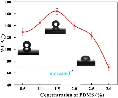
Figure 3.Variations of the WCA on the surface with different PDMS concentrations.

Figure 4.Variations of flashover voltages with different PDMS concentrations.
The results of the WCA measurements are shown in figure 3.The WCA increases first and then decreases with the increment of PDMS concentration.The WCA of the untreated ceramic is 69.9°.It rises to 129.1° with 0.5% PDMS added,indicating that the plasma with a small amount of PDMS can change the ceramic surface from hydrophilic to hydrophobic.The maximum WCA reaches 164°,superhydrophobic level,at the addition of 1.5% PDMS.The WCA decreases rapidly with a further increment of PDMS concentration.The WCA drops to 69° at the addition of 3.0% PDMS.These results demonstrate that the addition of PDMS at the appropriate concentration can effectively improve the hydrophobicity of the ceramic surface,while excessive addition results in a reverse effect.
The measurement results of the flashover voltage at different concentrations are shown in figure 4.The surface insulation strengths under dry and wet conditions show similar varying trends,which acquire maximum at the addition of 1.5% PDMS.When untreated,the dry and wet flashover voltages are 15.1 kV and 9 kV,respectively,meaning that the surface insulation capability decreases significantly after surface wetting.With the increase of PDMS concentration,the wet flashover voltage increases significantly,and reaches the maximum value 15 kV at the addition of 1.5% PDMS,66.7% higher than the untreated one.The difference between dry-wet flashover voltage is 2.3 kV,62.3% smaller than the untreated one.The wet flashover voltage begins to decrease rapidly with further increment of PDMS concentration.It can be concluded from the relationships between the flashover voltage and PDMS concentration that proper PDMS addition can improve the wet flashover voltage of ceramics more effectively than the dry flashover voltage.Combing the results of figures 3 and 4,it is found that the variations of the WCA are consistent with the wet flashover voltage under different PDMS concentrations.This result suggests that the improvement of the ceramic wet flashover voltage is dependent on the increase of surface hydrophobicity.The wet flashover voltage is dramatically improved for the superhydrophobic surface.The relationship between surface hydrophobicity and the wet flashover voltage will be given in the discussion section.
The charge density dissipation curves are shown in figure 5(a).The charge dissipation rate becomes slower with increasing PDMS concentration,indicating that the treated surface hinders the charge dissipation process.The trap energy level calculated from figure 5(a)is shown in figure 5(b).It can be seen that the trap energy level becomes deeper as the PDMS concentration increases.It increases from 0.97 eV of untreated ceramics to 0.985 eV when the PDMS concentration is 1.5%.As the treatment introduces deep traps,the deep traps lead to an enhanced ability to bind charges on the ceramic surface [24].The trap energy deviations are caused by changes in surface physio-chemical properties,which are tested and analyzed in the next section.
For engineering applications,the mechanical property is equally important as the electrical property.The mechanical property variations of the ceramics before and after the plasma treatment are evaluated with tensile strength,which defines the ability of a material to bear maximum load without failure or breaking [25].The tensile strengths of untreated and plasmatreated (PDMS concentration 1.5%) samples are measured with a universal force testing machine (CMT4503).The dumbbell-shaped samples are prepared for the tensile testing along with their dimensions as illustrated in figure 6(a),and the results are shown in figure 6(b).The tensile strengths for untreated and plasma-treated samples are respectively corresponding to 82.51 MPa and 81.50 MPa with the difference of 1.2%.No detectable variation of the mechanical property is observed from the tensile stress curves,proving the mechanical stability of the treatment.
4.Physical and chemical characterization
In this section,the surface physical methodology and chemical compositions are characterized,and the changes at different concentrations are compared to investigate the relationships between PDMS addition,surface physio-chemical properties,surface charge trap and flashover voltage.
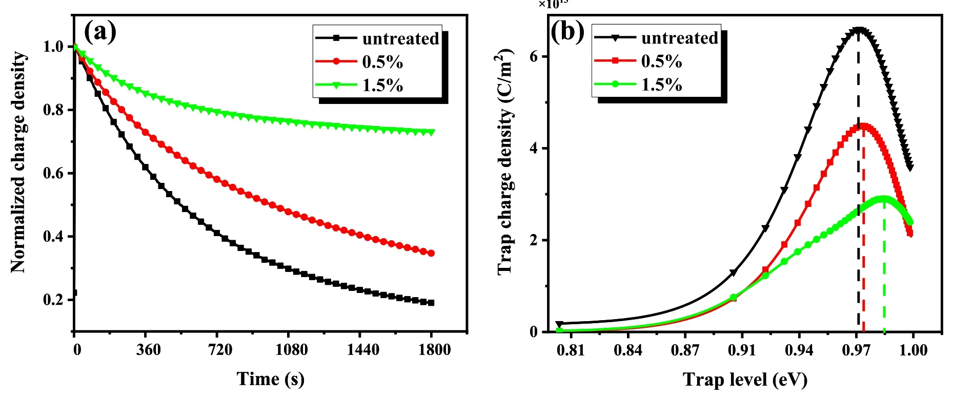
Figure 5.Surface charge measurement with different PDMS concentrations.(a)Charge density dissipation curves,(b)trap charge density curves.
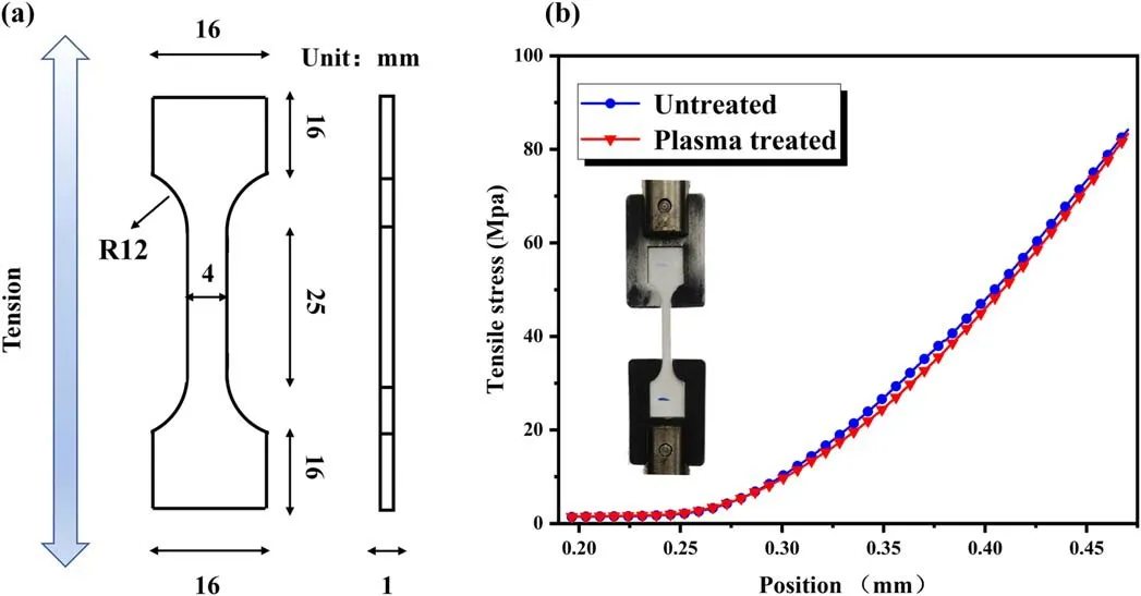
Figure 6.Tensile testing of the ceramics.(a)Sample structure,(b)testing results before and after the plasma treatment.
4.1.Physical properties
The SEM images at different PDMS concentrations are shown in figure 7.The untreated ceramic surface is flat overall with uniformly distributed micro-bumps,which is similar with the study by Yoichi Sato et al and Christian Bechteler et al [26,27].These micro projections are pebble-like particles with sizes ranging from 1 to 2 μm.This is the result of the growth of certain low surface energy grain weaving during ceramic sintering caused by the sintering process[28].Figure 7(b)shows the ceramic surface treated by plasma with a PDMS concentration of 0.5%.Some of the ceramic surface crystals are attached by nanoscale small particles,as shown in Region A.Some of the deposition products form agglomerates as shown in Region B.There are also locally formed thin films covering the crystal surface,as shown in Region C.This indicates that deposition occurs on the surface after PDMS fragmentation,forming deposits that aggregate and cross-link on the surface to form films.However,the deposited films cannot cover the entire crystal surface due to the low PDMS concentration.Figure 7(c)shows the ceramic surface after the PDMS treatment with 1.5% addition.A layer of dense coral-like structure appears on the ceramic surface,and the granular crystal structure of the ceramic completely disappears,indicating that the deposited film is thick enough to cover the entire ceramic surface due to sufficient PDMS addition.Figure 7(d) shows the ceramic surface at a magnification of 500 times when the concentration of PDMS is added at 3%.Irregular oil-like deposits of tens of microns scale are formed on the ceramic surface in several places,as shown in the Region D.It is presumed to be formed by the liquefied deposition of inactivated PDMS on the surface,which will be confirmed with XPS analysis.
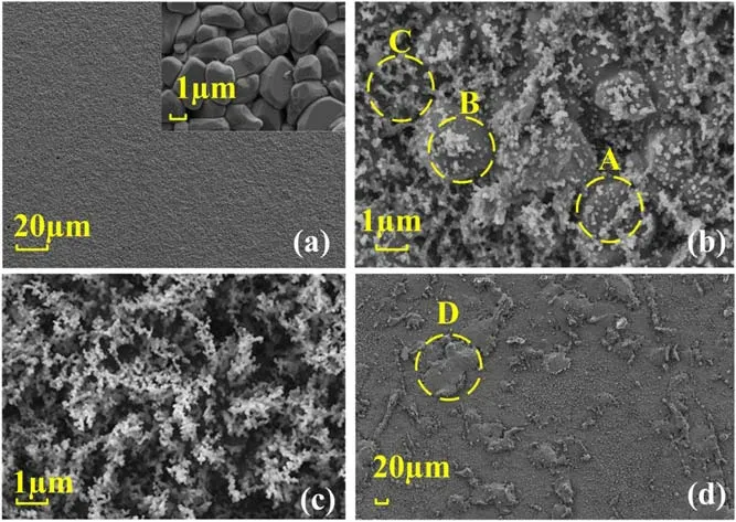
Figure 7.SEM images of ceramic surfaces at different concentrations of PDMS addition.(a)Untreated,(b)PDMS concentration of 0.5%,(c)PDMS concentration of 1.5%,(d)PDMS concentration of 3%.
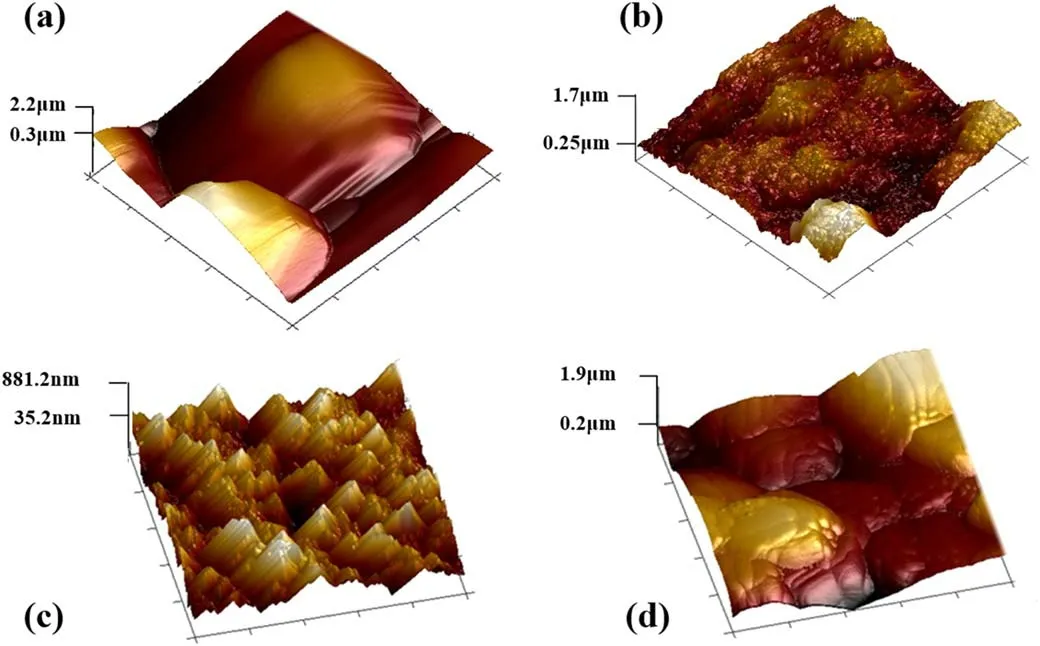
Figure 8.AFM images of ceramic surfaces at different concentrations of PDMS addition.(a)Untreated,(b)PDMS concentration of 0.5%,(c)PDMS concentration of 1.5%,(d)PDMS concentration of 3%.
The AFM images of ceramic surfaces treated with different PDMS concentrations are shown in figure 8.Bumps in micron scale are observed on the untreated ceramic caused by the crystalline textures.After a small amount of PDMS is added,dense tiny protrusions are formed on the surface and the grooves between the crystals are filled to some extent.The addition of 1.5% PDMS results in a large number of mountainous bumps on the surface with the height of hundred nanometer scale.With the addition of an excessive amount of PDMS,the ceramic surface recovers smoothly but is not flat.The change in ceramic surface morphology indicates that plasma treatment with different concentrations of PDMS can produce different morphologies on the ceramic surface.As shown in figures 7 and 8,the addition of PDMS produces discrete deposits on the ceramic surface.As the concentration of PDMS increases,the deposits gradually cross-link and aggregate,and a film with nano-scale bumps and micro-scale thickness can be deposited on the surface with proper amountof PDMS,covering the original crystal structure of the ceramic surface.
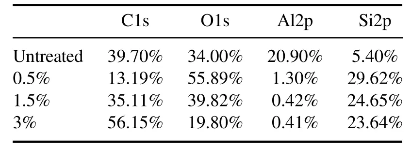
Table 1.Chemical composition ratios of ceramic surfaces with different PDMS concentrations.
4.2.Chemical properties
Tables 1 and 2 show the XPS results of full-spectrum and Si split-peak fitting results,respectively.Elemental peak of Si appears on the surface of the ceramics before treatment due to a small amount of SiO2doped as an additive in the alumina ceramic preparation process[29].When the precursor PDMS is added in the discharge region,chemical reactions occur between PDMS molecules and energetic particles in the plasma to generate PDMS fragments.These fragments are cross-linked and polymerized on the surface,leading to a dramatic increase of the content of Si element.Main reactions of the fragmentation and polymerization processes are shown in equations(3)-(6)[30].
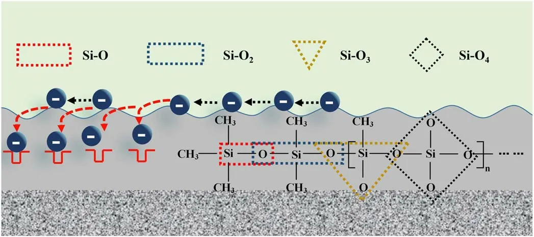
Figure 9.Influence of film physio-chemical properties on surface charge dissipation.
When the PDMS concentration is 0.5%,the Si element is mainly present in the form of Si-O4with the highest content of 85.1%,while the content of Si-O2and Si-O derived from PDMS molecules is negligible,indicating that the chemical composition of the film is mainly SiO2.The chemical bonds of SiO2inorganic films have lower polarity and are more conducive to improving hydrophobicity [31].However,due to micron-sized gullies between the crystals of the ceramic surface shown in figure 7,the deposits cannot fill all the gullies.When the PDMS concentration is increased to 1.5%,the Si-O2and Si-O3contents increase significantly to 13.4% and 41.7%,respectively,and the Si-O4content is reduced by nearly 50%,indicating that the chemical composition of the film is still dominated by Si-O3and Si-O4at a PDMS concentration addition of 1.5%.The reasons for the change in the chemical composition of the film are analyzed below.Studies have shown that the discharge intensity is weakened with overdoes precursor addition,inhibiting cross-linking of PDMS fragments.As a result,the Si-O4content decreases,and some of the PDMS fragments are deposited directly on the ceramic surface resulting in an increase of the Si-O2content.The WCA can reach 150°at a 1.5% concentration,which is higher than the results for a PDMS concentration of 0.5%.This is due to the formation of the dense coral-like micro-and nano-bump structure shown in figures 7(c)and 8(c) at 1.5% PDMS,which achieves both physical and chemical properties required for a superhydrophobic surface.When the concentration of PDMS is further increased to 3%,the ratio of C,Si,and O elements is close to 2:1:1 of PDMS molecules,verifying the SEM results shown in figure 7(d).Some of the PDMS in the discharge gap cannot be fragmented and liquefied to form oily droplets after reaching the ceramic surface.
The interpretation about the influence of film physiochemical properties on surface charge dissipation is shown in figure 9.The film deposited on the ceramic can introduce a large number of physical traps due to micro-nano mountainlike structures,and chemical traps due to the existence of silicon products.The electrons are trapped on the surface due to higher trap energy level.These trapped electrons weaken the electric field on the surface inhibiting the flashover.From the SEM results shown in figure 7(b),the Si-containing film coverage is incomplete at the addition of 0.5% PDMS,and the surface shows a mixed pattern of the ceramic and the film.Less deep traps are introduced compared with the surface fully covered by the film at the addition of 1.5% PDMS,which is unfavorable to the formation of a reverse electric field preventing the surface charge avalanche process.
5.Discussion
When PDMS is added,PDMS molecules are fragmented by energetic particles in the plasma(e.g.electrons,excited argon atoms,etc) to produce silicon-containing groups.Their deposition on the ceramic surface results in the formation of a rough low-polarity silicon film up to micron thickness,which ultimately changes the surface wet flashover voltage.The relationships between PDMS concentration,film physiochemical properties and hydrophobicity have been analyzed above.In this section,the relationship between the hydrophobicity and the wet flashover voltage of the deposited film on the ceramic surface will be discussed.
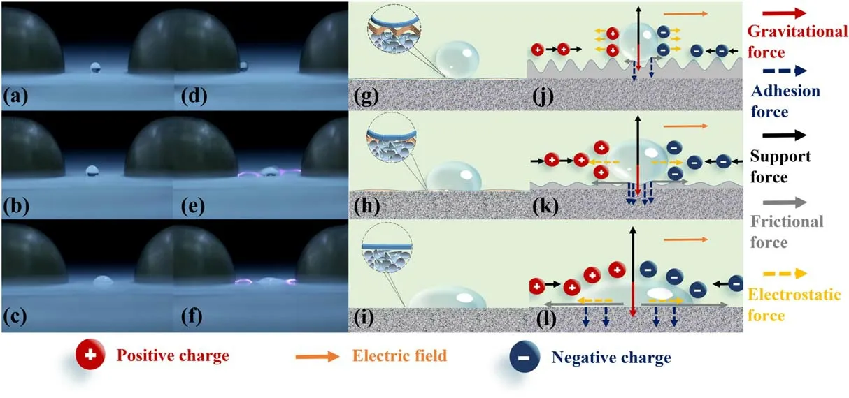
Figure 10.Relationship between surface hydrophobicity and the wet flashover,(a)-(f)images of droplet behavior on different surfaces,(a)and(d)superhydrophobic surface(1.5% PDMS)without and with the voltage applied between the electrodes,(b)and(e)hydrophobic surface(0.5% PDMS)without and with the voltage,(c)and(f)hydrophilic surface(before treatment)without and with the voltage;(g)-(i)mechanism of the droplet behavior on different surfaces,(g)and(j)superhydrophobic surface without and with the voltage,(h)and(k)hydrophobic surface without and with the voltage,(i)and(l)hydrophilic surface without and with the voltage.
According to the results in figures 3 and 4,the hydrophobicity of the film is directly related to the wet flashover voltage on the ceramic surface.Figures 10(a)-(f)exhibit the behaviors of water droplets on different surfaces between finger electrodes,which are taken with the camera(Canon EOS 6D)at the exposure time of 1/50 s.The droplet on the superhydrophobic surface is discovered to move towards the electrode driven by the electrostatic force,while it deforms on hydrophobic or untreated hydrophilic surface under multiple forces such as electrostatic force,surface adhesion force,and friction force.The wetting behavior directly affects the wet flashover voltage.Therefore,it is necessary to analyze the forces on the droplet as shown in figures 10(g)-(l).
When no voltage is applied between the finger electrodes,the droplets stay on the material surface by the adhesion force FAand gravity G,where the adhesion force is determined by the radius of the wetting area (r),the surface energy of the droplets (rp),and the surface energy of the material (rs) as shown in equation(7)[32-34]
The expression for the gravity of a droplet is as follows:
where ρ is the droplet density,g is the acceleration of gravity,and V is the droplet volume.
When a voltage is applied between the finger electrodes,motion of charged particles gathers on the droplet surface and generates internal electric field,as shown in figures 10(j)-(l).For non-ideally smooth material surfaces,the frictional force f of the water droplet can be expressed as follows
where μ is the friction coefficient of the material surface,whose value is in the range of 0.2-0.5 and does not differ much from the surface of different hydrophobic materials[35,36];is the electrostatic force in the vertical direction.
As shown in figure 10(g),the droplet basically remains spherical under the action of cavitation between micro-nano bumps of the film when the droplet is wetted on the surface with superhydrophobic ceramics.In this case,the effective contact radius r is quite small,and the droplet has very little adhesion to the superhydrophobic film according to equation(7).When the voltage between the finger electrodes reaches a certain value,the electrostatic force applied to the droplet is larger than the friction force,and the droplet moves rapidly toward the electrode with little liquid residue,producing a self-cleaning effect.When the droplet reaches the electrode,most of the surface area between the finger electrodes is still relatively dry,and the wet flashover voltage is close to the dry flashover voltage.It is worth noting that the wet flashover voltage is always lower than the dry flashover voltage due to the droplet adhering to the electrode as shown in figure 10(d).
When the droplet contacts the ceramic surface with a hydrophobic film,the droplet fills the space of ceramic particles not covered by the film.The surface adhesion increases significantly compared with the superhydrophobic coated surface due to large contact radius.When the voltage is applied,small movements of droplets occur on the material surface under the action of electrostatic force and adhesion force,accompanied by tensile deformation due to the inhomogeneity of both electric field distribution and ion distribution inside the droplet.When the applied voltage reaches a threshold,partial discharges occur in the dry region on both sides of the water droplet and further develop into flashover as shown in figure 10(e).When the droplet is wetted on the untreated ceramic surface,the adhesion force with the ceramic surface is large due to surface hydrophilicity.When the voltage is applied,the droplet is stretched and deformed by the electrostatic force,further enlarging the contact area and making it more difficult to overcome the frictional force as shown in figure 10(f).
Summarizing the relationship between surface hydrophobicity and the wet flashover from figure 10,the wetting area is dramatically reduced when the droplet is wetted on the superhydrophobic film.It moves toward the electrode under the action of the electrostatic force due to its low adhesion,leaving a large dry area between the electrodes,thus significantly increasing the wet flashover voltage.
6.Conclusion
In this work,a silicone film is deposited on the ceramic with Ar/PDMS DBD which significantly increases the wet flashover voltage.The film with micron thickness can fully cover the original crystalline textures on the ceramic surface at a PDMS addition ratio of 1.5%.The dry flashover voltage is increased for the introduction of deep traps.The self-cleaning effect of the superhydrophobic film occurs under the action of the applied voltage,significantly reducing the wetting area and increasing the wet flashover voltage.When the PDMS concentration is low,the film thickness is insufficient to cover the micron-sized ceramic crystal structure,although the WCA can still reach more than 120°.When the PDMS concentration is higher than 3%,excessive PDMS will condense on the ceramic surface to form oily droplets.
Acknowledgments
This work was partially supported by National Natural Science Foundation of China (Nos.51977104,52037004 and 52207160) and the Natural Science Foundation of Jiangsu Province(No.BK20220341).
猜你喜欢
Plasma Science and Technology(2022年5期)2022-06-01 07:55:32
Plasma Science and Technology(2021年6期)2021-06-21 02:00:22
Plasma Science and Technology(2021年6期)2021-06-21 02:00:02
书法赏评(2019年2期)2019-07-02 12:10:50
小天使·五年级语数英综合(2018年10期)2018-10-22 10:05:56
红领巾·探索(2018年4期)2018-05-21 11:55:08
小火炬·阅读作文(2017年5期)2017-07-07 12:32:44
西藏研究(2017年1期)2017-06-05 09:26:11
Transactions of Nanjing University of Aeronautics and Astronautics(2015年5期)2015-02-09 06:08:54
小天使·五年级语数英综合(2014年10期)2014-10-15 21:28:23
 Plasma Science and Technology2023年11期
- Plasma Science and Technology的其它文章
- High-order field theory and a weak Euler-Lagrange-Barut equation for classical relativistic particle-field systems
- Design of new resonant magnetic perturbation coils on the J-TEXT tokamak
- Non-invasive optical characterization and estimation of Zn porosity in gas tungsten arc welding of Fe-Al joints using CR model and OES measurements
- A study of grid failure mode drivers and methods for accelerated life testing of a 30cm diameter ion thruster
- Research on degradation mechanism of trichlorobenzene and Hg0 by nonthermal plasma catalysis
- Ionization wave propagation and cathode sheath formation due to surface dielectricbarrier discharge sustained in pulsed mode