
Proton induced radiation effect of SiC MOSFET under different bias
2023-11-02 08:13:36HongZhang张鸿HongXiaGuo郭红霞ZhiFengLei雷志锋ChaoPeng彭超WuYingMa马武英DiWang王迪ChangHaoSun孙常皓FengQiZhang张凤祁ZhanGangZhang张战刚YeYang杨业WeiLv吕伟ZhongMingWang王忠明XiangLiZhong钟向丽andXiaoPingOuyang欧阳晓平
Chinese Physics B 2023年10期
关键词:王迪
Hong Zhang(张鸿), Hong-Xia Guo(郭红霞),,†, Zhi-Feng Lei(雷志锋), Chao Peng(彭超), Wu-Ying Ma(马武英),Di Wang(王迪), Chang-Hao Sun(孙常皓), Feng-Qi Zhang(张凤祁), Zhan-Gang Zhang(张战刚), Ye Yang(杨业),Wei Lv(吕伟), Zhong-Ming Wang(王忠明), Xiang-Li Zhong(钟向丽), and Xiao-Ping Ouyang(欧阳晓平),
1School of Material Science and Engineering,Xiangtan University,Xiangtan 411105,China
2Science and Technology on Reliability Physics and Application of Electronic Component Laboratory,Electronic Product Reliability and Environmental Testing Research Institute,Guangzhou 510610,China
3Northwest Institute of Nuclear Technology,Xi’an 710024,China
Keywords: proton,silicon carbide metal-oxide-semiconductor field-effect transistor(SiC MOSFET),degradation,defect,ionization radiation damage
1.Introduction
Silicon carbide (SiC) is famous for its excellent material properties.As one of the most representative thirdgeneration semiconductor devices, SiC power devices have attracted much attention from the birth to the realization of commercial applications.[1,2]With the maturity of the device manufacturing process,SiC power devices are more and more used in power conversion systems.With the continuous development of science and technology,people have accelerated the pace of space exploration,and put forward higher requirements for space electronic power systems.High power devices are required to realize the construction of high voltage and high power systems,compared with silicon power devices with the same power density,SiC power devices have smaller volume,conduction resistance and better heat dissipation performance.
A large number of studies have shown that the presence of protons, neutrons and heavy ions can induce single event effects in SiC diodes and metal-oxide-semiconductor fieldeffect transistor(MOSFET).[3-11]Richard Det al.showed that when the proton cumulative fluence reaches 1×10¹⁴p·cm-2,the forward characteristic of the SiC diode will be obviously degraded, while the reverse characteristic is not affected.[12]Both SiC MOSFET and SiC diode are SiC devices that have been commercially applied, the structure of SiC MOSFET is more complex than that of SiC diode.At the same time, SiC MOSFET has more operating bias states than SiC diode.With the accumulation of proton fluence,the radiation effect of SiC MOSFET under different bias voltages is still unclear.Proton induced single-event gate rupture(SEGR)and single event burnout(SEB)under high bias voltage are serious problems to be solved at present, radiation damage caused by proton fluence accumulation under different bias conditions cannot be ignored.
In this paper,based on the proton with energy of 20 MeV,we had carried out the research of proton radiation effect under different bias conditions.Before and after irradiation,we measured the electrical properties of SiC MOSFETs under different radiation bias conditions,and further analyzed the defects induced by proton radiation based on deep level transient spectroscopy(DLTS).Using Monte Carlo simulation,we analyzed the ionizing radiation damage and non-ionizing radiation damage in SiC MOSFET induced by proton irradiation.
2.Proton cumulative irradiation experiment
The device we selected is a planar SiC MOSFET C3M0120090D produced by CREE.The proton irradiation experiment is carried out in the Xi’an 200 MeV Proton Application Facility(XiPAF),which can directly extract the proton beam with energy of 20 MeV.The internal structure and material composition of the devices selected in this paper are consistent with those in Ref.[13].In the experiment,protons are incident perpendicularly from the front of SiC MOSFET,and then successively pass through the aluminum metal source electrode, SiO2, polysilicon gate, oxide, SiC epitaxial layer and substrate.
In the experiment,we carry out proton irradiation experiments under four typical bias conditions,as shown in Table 1.When SiC MOSFETs are used as power conversion devices in electronic power systems,they can be divided into four cases according to voltage bias conditions.When the whole electronic power system is turned off,the devices are in static bias.When the system is running,SiC MOSFET has three bias conditions, namely, drain bias, gate bias and turn-on bias.When the bias voltage is applied to only one electrode in the experiment,the other two electrodes are grounded.

Table 1.Different proton irradiation bias conditions.
The current of SiC MOSFET is monitored in real time when the bias voltage is applied, as shown in Fig.1.The real-time current of SiC MOSFET is small under gate bias and drain bias, and has no obvious change with the increase of proton fluence.Under the turn-on bias, the real-time current of SiC MOSFET increases linearly with the increase of proton fluence.

Fig.1.Variation of SiC MOSFET real-time current with proton cumulative fluence under different bias conditions.
3.Experimental results and analysis
3.1.Electrical characteristics test
Before and after proton irradiation, we test the electrical characteristics of SiC MOSFETs under different radiation bias conditions.The test instrument is the Agilent B1500 semiconductor analyzer.The transfer characteristics and transconductance of SiC MOSFETs under different radiation bias conditions are shown in Fig.2.The threshold voltage of SiC MOSFETs with different bias conditions has a negative shift under proton cumulative irradiation.The transconductance peak value of SiC MOSFET also increases and shifts to varying degrees.The transconductance peak value of devices under proton irradiation with gate bias increases most, while the transconductance change of irradiated devices is minimal under static bias.The threshold voltage degradation of SiC MOSFET is shown in Table 2.Under the gate bias,the threshold voltage of the device has a negative shift of 0.27 V,while the threshold voltage of the device with static bias has a negative shift of 0.13 V under the same proton cumulative fluence.Under drain bias and turn-on bias, devices with the same proton cumulative fluence have similar threshold voltage shifts.Because of the negative shift of the threshold voltage, the channel opening ability is enhanced under the same gate voltage.Therefore, the drain current of SiC MOSFET increases linearly with the increase of the proton cumulative fluence under the turn bias in Fig.1.

Fig.2.Electrical characteristics of SiC MOSFET under different bias conditions: (a)transfer characteristics,(b)transconductance.

Table 2.SiC MOSFET parameters under different radiation bias conditions.
Figure 3 shows the gate leakage current and breakdown characteristics of SiC MOSFET before and after irradiation.As shown in Fig.3(a), the gate current of devices before and after irradiation fluctuates in the order of picoamps,and there is no significant difference in the gate current under different bias conditions.As shown in Fig.3(b),the cumulative proton fluence reaches 2×10¹¹p·cm-2, and the breakdown voltage of SiC MOSFET with different biases does not change.

Fig.3.Electrical characteristics of SiC MOSFET under different bias conditions: (a)gate leakage current;(b)breakdown characteristic.
There is an equivalent relationship between the total ionization dose effect caused by cumulative proton irradiation and gamma irradiation,the equivalent conversion formula is[14]
where TIDgammarepresents the ionization damage dose caused by gamma irradiation, and its unit is rad(Si).LET represents the linear energy transport of the corresponding proton in the Si material, and its unit is MeV·cm2·mg-1;Nprotonstands for cumulative proton fluence.Proton energy and proton cumulative fluence jointly affect the total ionization dose.According to the calculation results of SRIM software,[15]the LET value of 20 MeV proton in silicon is 0.0203 MeV·cm2·mg-1.The cumulative fluence of proton irradiation in the experiment is 2×10¹¹p·cm-2,so the proton equivalent gamma total ionization dose is 64.96 krad(Si).Using the Co-60 radiation source of the Shanghai Institute of Applied Physics,we carry out gamma irradiation experiments of the same type of SiC MOSFET under static bias, the gamma total ionization dose is 64.96 krad(Si).The transfer curve and transconductance changes of SiC induced by Gamma irradiation are shown in Fig.4.The threshold voltage of SiC MOSFET shifts to the left about 0.14 V under gamma irradiation, and the transconductance peak increases slightly.Under the equivalent total ionizing dose, the degradation trend of SiC MOSFET in gamma irradiation and proton accumulation irradiation is consistent,and the gate and breakdown characteristics of SiC MOSFET do not change.
On the other hand,based on the neutron pulse reactor of the Northwest Institute of Nuclear Technology, we carry out experiments on equivalent 1 MeV neutron displacement damage effect of SiC MOSFET under different bias conditions,[16]the cumulative neutron fluence reaches 1×10¹⁴n·cm-2, the experimental results are shown in Fig.5.The threshold voltage of SiC MOSFET is not degraded under static bias and turn-on bias,while the threshold voltage of SiC MOSFET is shifted to the right under drain bias,and the degradation trend is opposite to that under proton irradiation.Combined with the results of the gamma experiment and equivalent 1 MeV neutron irradiation experiment,the effect of proton cumulative irradiation on the performance of SiC MOSFET is mainly due to ionization radiation damage.
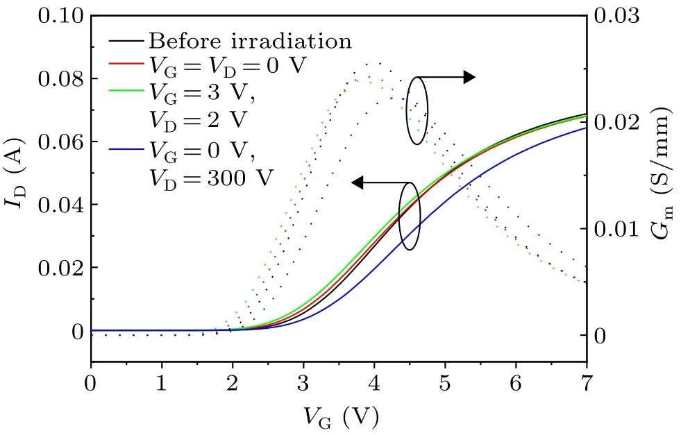
Fig.5.Electrical characteristics of SiC MOSFET under the equivalent 1 MeV neutron irradiation:(a)transfer characteristics;(b)transconductance.
3.2.Deep level transient spectrum test
Deep level transient spectroscopy(DLTS)is an effective method to analyze deep level defects in semiconductor devices,which can be used to analyze the changes in deep level defects induced by proton irradiation in SiC MOSFETs.The deep level defects of SiC MOSFETs are tested before and after irradiation using the deep level transient spectrum instrument produced by Phystech company.In the DLTS test,the temperature range is 50 K-450 K,the gate electrode is connected to the positive electrode,the source electrode is connected to the negative electrode,and the drain electrode is connected to the ground.The pulse time is 1 ms,the cycle time width is 4 ms,the reverse voltage is 0 V,and the pulse voltage is 6 V in the DLTS test.
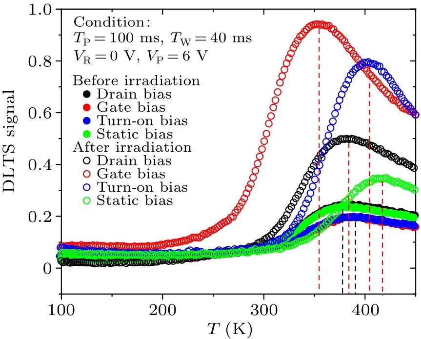
Fig.6.DLTS signal spectrum of SiC MOSFET before and after proton irradiation under different radiation bias conditions.
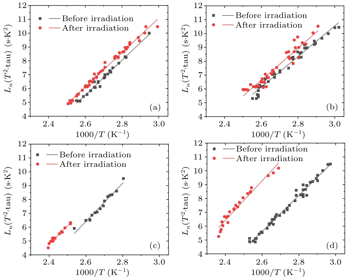
Fig.7.Arrhenius curve of SiC MOSFET before and after proton irradiation under different bias conditions: (a)drain bias;(b)gate bias;(c)turn-on bias;(d)static bias.
DLTS signal spectra of SiC MOSFETs under different bias conditions are shown in Fig.6.DLTS signal spectrum results show that the defect type of SiC MOSFET C3M0065120D is mainly ON2 (Ec-1.1 eV) center, which exists on the surface of C implanted SiC and oxide-SiC interface, and still exists after high temperature annealing at 1800°C.[17-19]According to the DLTS signal spectrum, the Arrhenius curves of devices before and after irradiation under different bias conditions are obtained through further processing,as shown in Fig.7.The defect energy level,defect capture cross sectionσnand defect concentrationNTof SiC MOSFET extracted from the Arrhenius curve are shown in Table 3.After proton irradiation under different bias conditions, the defect energy level of SiC MOSFET fluctuates to some extent, but the defect type does not change.The concentration and the capture cross section of the defects increase after proton irradiation under different bias conditions.Under the gate bias,the concentration and capture cross section of the defect increase more obviously than those under the other three kinds of radiation bias, which results in a more obvious threshold voltage shift and transconductance change of SiC MOSFET as shown in Fig.2.The theoretical calculation results of the researchers show that,the main defect type in the defect center ON2(Ec-1.1 eV)is carbon inversion-carbon vacancy pair(CSiVc).[19-22]

Table 3.Information about defects of SiC MOSFET under different bias conditions.
The deep level transient spectrum test results of SiC MOSFET before and after gamma irradiation are shown in the Fig.8.Under equivalent ionizing dose, the DLTS signal of SiC MOSFET before and after gamma irradiation is consistent with that of proton irradiation.The defect type of SiC MOSFET does not change before and after gamma irradiation,but the defect concentration and defect cross section of SiC MOSFET increase to some extent.The types of defects induced by cumulative proton irradiation and gamma irradiation under the same equivalent ionizing dose are also the same,and the variation of defects before and after irradiation shows the same trend.No matter whether under gamma irradiation or proton accumulation irradiation, the ionizing radiation damage cannot produce displacement defects such as vacancy or gap atoms, but the holes generated by ionizing radiation are trapped by the interface state traps at the interface of SiO2and SiC due to low mobility, resulting in the DLTS test results showing that the defect concentration and defect capture cross section of SiC MOSFET increase, and the defect type does not change.

Fig.8.DLTS test result of SiC MOSFET before and after gamma irradiation: (a)DLTS signal spectrum,(b)Arrhenius curve.
4.Analysis and discussion
4.1.Monte Carlo simulation of proton transport
When 20 MeV protons incident on SiC MOSFET,in addition to the energy loss caused by direct ionization, it also includes the energy loss induced by secondary particles generated by nuclear reaction.Proton energy loss includes ionization energy loss and non ionization energy loss.The ionization energy loss(IEL)can reflect the ionization damage degree of SiC MOSFET, while the non-ionization energy loss (NIEL)reflects the displacement damage effect.Based on the Monte Carlo method, we use the GEANT4 simulation tool[23,24]to carry out the proton irradiation simulation of SiC MOSFET.Figure 9(a) shows the device model and parameter information used in the GEANT4 simulation.Figure 9(b) shows the transport process of protons inside the device.The blue line represents the movement track of protons, and the red line represents the movement track of secondary electrons.In addition,protons will also react with device materials to produce secondary heavy ions.The transport of protons and secondary particles in devices and the formation of ionization energy loss and non ionization energy loss on their tracks.
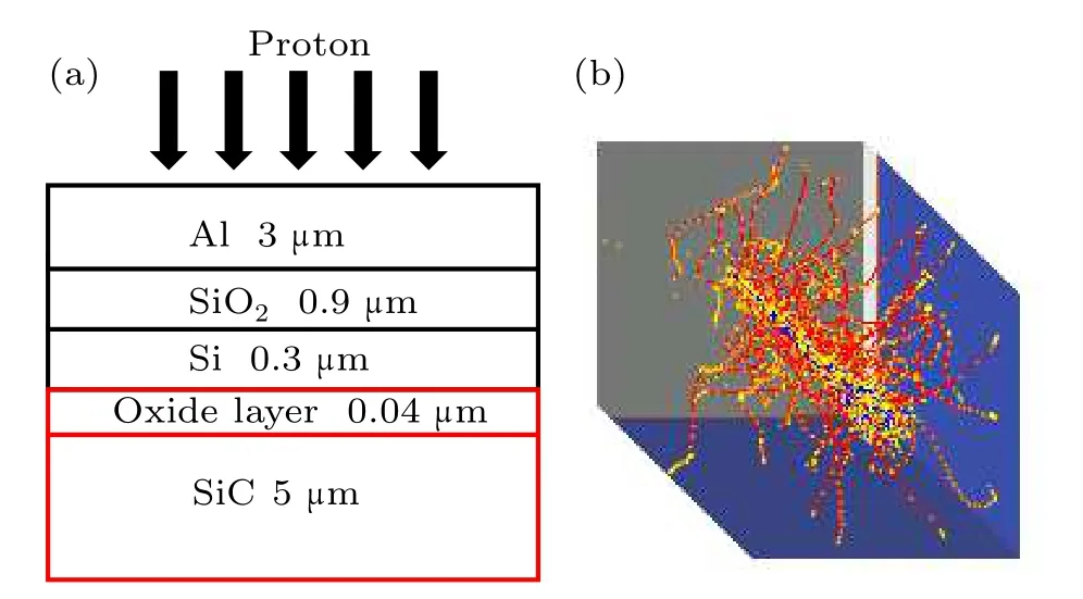
Fig.9.GEANT4 simulation: (a)SiC MOSFET device model;(b)transport of 20 MeV protons in SiC MOSFETs.
Through Monte Carlo simulation, the ionization energy loss and non-ionization energy loss of protons and their secondary particles in the device are calculated as shown in Fig.10.The ionizing energy loss caused by proton incident in the device is more than two orders of magnitude higher than non-ionizing energy loss.The main reason for the change in the electrical performance of the device is the ionization energy loss.The total dose effect corresponding to ionization energy loss has the strongest influence on SiC MOSFETs under the gate voltage bias.[25]As the non-ionization energy loss is small,we obtain that the change of defect concentration and defect capture cross section of the device in the DLTS test are mainly due to the ionization energy loss.When SiC MOSFET is working, the current flows from the drain to the substrate,the epitaxial layer,and from the channel to the source region.The defects in the oxide layer and the oxide-SiC interface seriously affect the electrical properties of devices.
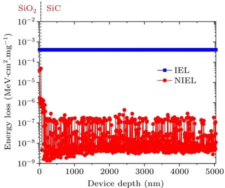
Fig.10.Distribution of ionization energy loss and non-ionization energy loss in SiC MOSFET induced by 20 MeV proton.
Under the static bias condition, there is no electric field inside the device.Under the other three bias conditions, the oxide layer and the epitaxial layer of SiC MOSFET have different electric fields.The existence of electric fields will affect the recombination and movement of electrons and holes,thereby affecting the formation of defects.From the experimental results, the existence of an internal electric field leads to more serious degradation of SiC MOSFET.At the same time, because SiC MOSFET is a vertical device, the electric field inside the device under drain bias is mainly concentrated in the epitaxial layer,while when the gate has bias voltage, there is a strong electric field inside the oxide layer and near the oxide-SiC interface, which results in the strongest change of defect concentration and defect capture section of SiC MOSFET under the same proton fluence.
When the cumulative fluence reaches 1×10¹⁴n·cm-2,the non-ionizing energy loss induced by equivalent 1 MeV neutrons is shown in Fig.11.The active area of SiC MOSFET is about 0.021 cm2,and the maximum value of NIEL in the SiO2oxide layer is less than 10-1MeV·cm2·mg-1when the accumulated neutron fluence reaches 1×10¹⁴n·cm-2.In SiC material,the NIEL peak appears at the interface of the oxide layer and SiC material,and the NIEL decreases gradually with the increase of depth.The NIEL induced by an equivalent 1 MeV neutron with a cumulative fluence of 1×10¹⁴n·cm-2is much larger than that of 20 MeV proton with a cumulative fluence of 2×10¹¹p·cm-2.However,according to the test results of electrical properties,the degradation of transfer properties of SiC MOSFET only appears under drain bias when the equivalent 1 MeV neutron fluence reaches 1×10¹⁴n·cm-2.Combined with the experimental and simulation results of equivalent 1 MeV neutrons, it is shown that SiC MOSFET has a strong resistance to displacement damage, and on the other hand, it is also shown that NIEL has little influence on the proton radiation damage of SiC MOSFET.
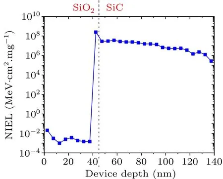
Fig.11.Distribution of non-ionization energy loss in SiC MOSFET induced by 1 MeV neutron.
Combine the active area of SiC MOSFET, when the cumulative proton fluence reaches 2×10¹¹p·cm-2, the proton fluence vertically incident from the active region is about 4.2×10⁹p·cm-2.The ionization damage doseDper unit depth inside the device can be calculated by
where the unit ofDis rad,EIELis the ionization energy loss per unit depth,and its unit is MeV·cm2·mg-1.NPis proton fluence per unit area,and its unit is p·cm-2.The calculated ionization damage dose of 20 MeV proton in the device is about 1.3 krad.At the same time,we use GEANT4 to simulate and calculate the internal ionization damage dose of devices under several typical proton energies,as shown in Fig.12.With the increase of proton energy, the ionization damage caused by direct ionization of protons and secondary particles decreases,which means that the proton radiation effect in SiC MOSFETs is weaker under the irradiation of higher energy protons.Under low bias voltage, the single event effect cross section of SiC MOSFET is low,[6]but the accumulated proton fluence is high,which may also lead to a negative shift of threshold voltage,or even lead to channel opening,affecting the evaluation of the proton single event effect in SiC MOSFET.The ionization damage induced by proton needs to be evaluated when it is used to study the single event effect of SiC MOSFET.
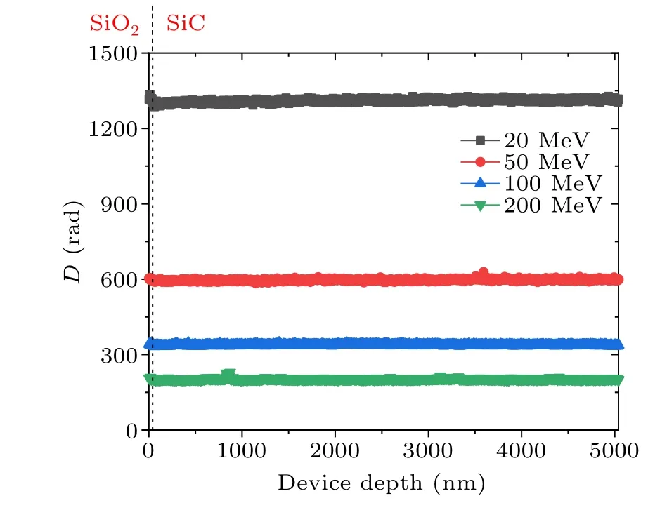
Fig.12.Ionization energy loss of protons with different energies in SiC.
4.2.Effect of bias condition on SiC MOSFET
The internal structure and material composition of SiC MOSFET are obtained by reverse analysis.Based on the reverse analysis results, the TCAD model of SiC MOSFET is constructed.The specific model and production batch of SiC MOSFET are consistent with SiC MOSFET used in the Ref.[13],so the structure and parameters of the TCAD model of SiC MOSFET constructed by us are consistent with those in the Ref.[13].In the simulation, we do not consider the electric thermal model,and other physical models are considered.The TCAD model of SiC MOSFET is shown in Fig.13.The TCAD model of SiC MOSFET contains 5 cells.The gray part represents the source metal,the red-brown part represents SiO2, the white part surrounded by SiO2represents the gate electrode, and the yellow part represents the epitaxial layer.The substrate is below the epitaxial layer, and the bottom of the substrate is the drain electrode of the SiC MOSFET.

Fig.13.TCAD model of SiC MOSFET.
We apply different voltages to the electrodes of SiC MOSFET according to experimental bias conditions.The twodimensional distribution and one-dimensional distribution of the electric field in SiC MOSFET under different bias conditions are shown in Fig.14.Under the drain bias, there is a large electric field in the epitaxial layer of SiC MOSFET and the oxide layer.The electric field in the oxide layer makes the holes induced by ionization radiation damage in the oxide layer move away from the interface between the oxide layer and SiC,while the electric field in the epitaxial layer promotes the holes in the epitaxial layer to move towards the interface between the oxide layer and SiC.Under gate bias,the direction of the electric field diffuses outward from the gate electrode.The higher electric field is mainly concentrated in the oxide layer, the holes in the oxide layer move toward the interface between the oxide layer and SiC, and the electric field in the epitaxial layer is small.Under the turn-on bias, there is an electric field in the oxide layer with the same direction as that under the gate bias,while the electric field in the epitaxial layer is small because the drain voltage is small and the current is formed in SiC MOSFET.

Fig.14.The internal electric field distribution of SiC MOSFET under different bias conditions: (a) two-dimensional distribution; (b) onedimensional distribution cut at x=0.
As shown in Fig.14(b),the peak electric field intensity in the oxide layer of SiC MOSFET caused by drain bias is nearly three times than that of the oxide layer under turn-on bias,and the difference between the peak electric field intensity of the oxide layer under drain bias and that under gate bias is small.However, combined with the results of the electrical characteristics test and defect test,the degradation of SiC MOSFET under drain bias and turn-on bias is similar,while the degradation under gate bias is the most serious.The ionizing radiation damage induced by a proton in SiC MOSFET is affected by the intensity of the electric field of the oxide layer and SiC epitaxial layer,and also by the direction of the electric field.
5.Conclusion
Based on the Xi’an 200 MeV Proton Application Facility, the radiation effect of SiC MOSFETs with different bias conditions under 20 MeV proton irradiation is studied.When cumulative proton fluence reaches 2×10¹¹p·cm-2, the electrical properties of SiC MOSFETs irradiated under drain bias,gate bias, turn-on bias and static bias have changed, mainly reflected in the negative shift of threshold voltage and the increase of the peak of transconductance.The threshold voltage shift of SiC MOSFETs is the most serious under the gate bias.The gate leakage current and breakdown voltage of SiC MOSFETs do not change significantly after irradiation.DLTS test results show that the proton radiation effect increases the defect capture cross section and defect concentration of SiC MOSFET, and the defect type does not change.Among the four bias conditions,the change of defect capture cross section and defect concentration before and after proton irradiation is the largest under gate bias.The degradation trend and defect change of SiC MOSFET under proton cumulative irradiation and equivalent gamma total ionizing dose are the same.Based on the Monte Carlo simulation, we carry out a proton transport simulation in SiC.The ionization energy loss of 20 MeV protons and their secondary particles in the SiC MOSFET oxide layer and SiC layer is more than two orders of magnitude higher than the non ionization energy loss, the proton radiation effect mainly causes ionization damage to devices.With the increase of proton energy, the ionization energy loss induced by proton radiation in SiC MOSFET becomes smaller and smaller.By comparing the internal electric field of SiC MOSFET at different bias voltages,the proton radiation damage of SiC MOSFET is affected by the intensity and direction of the electric field in the oxide layer and epitaxial layer.When conducting proton single event effect research on some devices with low single event effect cross section, the influence of radiation effect at high proton fluence on single event effect analysis needs to be evaluated.
Acknowledgment
Project supported by the National Natural Science Foundation of China(Grant No.12075065).
猜你喜欢
——布加迪CHIRON PROFILÉE
世界汽车(2023年1期)2023-03-14 03:13:48
——兰博基尼HURACÁN TECNICA
世界汽车(2022年7期)2022-08-08 08:51:30
世界汽车(2022年6期)2022-07-13 04:25:00
世界汽车(2022年6期)2022-07-13 04:24:38
——2023 HYUNDAI PALISADE
世界汽车(2022年5期)2022-06-10 10:18:10
——丰田GR COROLLA
世界汽车(2022年5期)2022-06-10 10:18:06
——雷克萨斯RZ
世界汽车(2022年5期)2022-06-10 10:18:00
——法拉利296 GTS
世界汽车(2022年5期)2022-06-10 10:17:50
——宾利MULLINER BENTAYGA SPEED
世界汽车(2022年4期)2022-05-14 08:34:04
阅读(快乐英语高年级)(2021年12期)2021-05-30 16:51:30

- Chinese Physics B的其它文章
- Corrigendum to“Reactive oxygen species in plasma against E.coli cells survival rate”
- Dynamic decision and its complex dynamics analysis of low-carbon supply chain considering risk-aversion under carbon tax policy
- Fully relativistic many-body perturbation energies,transition properties,and lifetimes of lithium-like iron Fe XXIV
- Measurement of the relative neutron sensitivity curve of a LaBr3(Ce)scintillator based on the CSNS Back-n white neutron source
- Kinesin-microtubule interaction reveals the mechanism of kinesin-1 for discriminating the binding site on microtubule
- Multilevel optoelectronic hybrid memory based on N-doped Ge2Sb2Te5 film with low resistance drift and ultrafast speed