Epitaxial growth of trilayer graphene moir´e superlattice
Yalong Yuan(袁亚龙), Yanbang Chu(褚衍邦), Cheng Hu(胡成), Jinpeng Tian(田金朋), Le Liu(刘乐),Fanfan Wu(吴帆帆), Yiru Ji(季怡汝), Jiaojiao Zhao(赵交交), Zhiheng Huang(黄智恒),Xiaozhou Zan(昝晓洲),Luojun Du(杜罗军), Kenji Watanabe, Takashi Taniguchi, Dongxia Shi(时东霞),3,Zhiwen Shi(史志文), Wei Yang(杨威),7,†, and Guangyu Zhang(张广宇),7,‡
1Beijing National Laboratory for Condensed Matter Physics and Institute of Physics,Chinese Academy of Sciences(CAS),Beijing 100190,China
2School of Physical Sciences,University of Chinese Academy of Sciences,Beijing 100190,China
3Key Laboratory of Artificial Structures and Quantum Control(Ministry of Education),School of Physics and Astronomy,Shanghai Jiao Tong University,Shanghai 200240,China
4Collaborative Innovation Center of Advanced Microstructures,Nanjing 210093,China
5Research Center for Functional Materials,National Institute for Materials Science,1-1 Namiki,Tsukuba 305-0044,Japan
6International Center for Materials Nanoarchitectonics,National Institute for Materials Science,1-1 Namiki,Tsukuba 305-0044,Japan
7Songshan Lake Materials Laboratory,Dongguan 523808,China
Keywords: epitaxial growth,ABC-TLG/hBN moir´e superlattice,electron correlations
Graphene-based moir´e superlattices have been demonstrated as ideal flat band systems for investigating correlated physics.[1–19]Among them,a moir´e superlattice of ABC stacked trilayer graphene(ABC-TLG),[7,20–22]by aligning its lattice with the hexagonal boron nitride (hBN) substrate, has attracted considerable attention.As a matter of fact, the band structure of ABC-TLG itself is quite flat with field tunable van Hove singularities (vHS) near the band edge,contributing to various symmetry broken metalic phases and superconductivity.[23,24]Moreover, with the introducing of a long wavelength periodic potential in ABC-TLG/hBN hetero moir´e superlattice, isolated flat moir´e bands near the charge neutral point are generated at finite displacement field,which eventually leads to the discovery of correlated insulators, superconductivity, and anomalous quantum Hall effect in this system.[7,20–22]Compared to the twisted bilayer graphene,ABC-TLG/hBN moir´e superlattice have more freedom on the twist angle control.Thus far,ABC-TLG/hBN moir´e superlattice is highly relied on the complicated pick-up transferring,and a technique capable of fabricating moir´e superlattice for easy production with a large scale is high demanded.
In this work,we directly obtain TLG/hBN moir´e superlattice by epitaxy.The epitaxial grown trilayer graphene and the hBN substrate are aligned,giving a moir´e period of∼15 nm.We fabricate the epitaxial TLG into devices with a dual gate configuration.The transport results show that the TLG has the characteristics of ABC stacking order,supported by the presence of a band gap of 1.2 meV at the charge neutral point and the quantum Hall states with Landau levels filling factors of ofν=6,10,14,....In addition,we observe a resistance peak at half filling at a finite displacement field,implying the presence of strongly correlation in our epitaxial grown ABC-TLG/hBN moir´e superlattice.
Figure 1(a)is a schematic diagram of the epitaxial trilayer graphene on hBN substrates, and figure 1(b) is the resulted moir´e superlattice structure measured from atomic force microscopy (AFM) imaging.The growth of TLG is carried out in a remote plasma-enhanced chemical vapour deposition system(r-PECVD).Before growth,hBN flakes are mechanically exfoliated onto a 300-nm-thick SiO2/Si.During the growth,methane (CH4) is used as the feed gas, with a low growth pressure of 0.2 Torr (1 Torr=1.33322×10⁵Pa).Assisted by the plasma technique, methane can be decomposed into various reactive radicals, from which the carbon or hydrocarbon radicals allowing the nucleation and growth of graphene and the hydrogen radicals can remove amorphous carbon and ensure sp2carbon growth.[25–27]At an optimal temperature (T)of∼500◦C,we can achieve epitaxial growth of single-domain graphene as previously reported.[28–30]Figures 1(c)–1(f)show the epitaxy of TLG/hBN moir´e superlattice at different growth stages.At the nucleation stage, monolayer graphene islands are randomly formed on the hBN surface.As carbon atoms are continuously deposited onto the surface, the existing nuclei grow and connect (Fig.1(c)), which eventually produces a continuous and uniform graphene film with second-layer graphene islands grown on top (Fig.1(d)).By extending the growth time,the second layer graphene also forms a continuous bilayer graphene film topped with islands of the third-layer(Fig.1(e)), which then gradually grow and coalesce to produce a continuous trilayer graphene film with a small amount of the fourth-layer islands on top (Fig.1(f)).In our epitaxial grown TLG on hBN, we observed a clear moir´e pattern with a period of 15 nm using AFM (Fig.1(b)).The resulted moir´e periodicity in TLG/hBN agrees well with that in epitaxial monolayer graphene/hBN moir´e superlattice from our previous reports;[28–30]and thus, we attribute the superlattice to the lattice mismatch between TLG and hBN at zero rotation angle.

Fig.1.Epitaxial trilayer graphene growth on hBN.(a)Schematic diagram of epitaxial growth structure.(b)Moir´e pattern of epitaxial trilayer graphene/hBN superlattice.(c)–(f) AFM images of as-grown graphene on hBN at different stages including small grains nucleation and coalescence of grains(c), continuous monolayer graphene with some second-layer nuclei on top(d), continuous bilayer graphene with some third-layer nuclei on top(e),and continuous trilayer graphene with some fourth-layer nuclei on top(f).
We now turn to the electrical properties of the epitaxial trilayer graphene grown on hBN.Another hBN flake was stacked on the TLG/hBN structure for encapsulation and as a top-gate dielectric.The device was then etched into a Hall bar structure using standard electron-beam lithography techniques, and Cr/Au was deposited for contacts and top gate electrodes.[31]Our devices have a dual gate configuration,which allows independent tuning of the carrier densitynand displacement fieldD.Here,n=(CBGVBG+CTGVTG)/eandD=(CBGVBG−CTGVTG)/2ε0, whereCBG(CTG) is the geometrical capacitance per area for bottom (top) gate,eis the electron charge, andε0is the vacuum permittivity.All measurements are done atT=1.8 K unless stated otherwise.
The measured the longitudinal resistance(Rxx)as a function of the bottom gate (VBG) and top gate (VTG) is shown in Fig.2(a).We can observe the obvious resistance peak at the charge neutral point(CNP),and the resistance increases with the increase of the displacement fieldD.Figure 2(d) shows the temperature dependence ofRxx(n) atD=0.The resistivity peak at CNP exhibits typical insulating behavior,i.e.,Rxxincreases asTdecreases.The extracted thermally activated bandgap(∆)at CNP is of 1.2 meV atD=0, and it increases with the increase ofDas shown in Fig.2(f).Trilayer graphene has two stable stacking orders in its natural form:ABA (Bernal) and ABC (rhombohedral).The ABC trilayer graphene is a semiconductor with a gate-tunable band gap,while the ABA trilayer graphene is a gapless semimetal.[32–36]The observations of the gap opening at CNP and its field tunability agree well with transport characteristics of ABC(rhombohedral)stacked TLG.
In addition to the resistance peak at CNP, we also observed the resistance peaks at aroundn=±1.92×1012cm−2in Fig.2(d).Such resistance peaks become barely discernible atT>30 K, and the temperature dependence also exhibits insulating behavior (as shown in Fig.2(e)).In principle,similar to the epitaxial graphene/hBN superlattice[28–30]and transferred ABC-TLG/hBN superlattice,[7,20,21]the epitaxial TLG/hBN superlattice would introduce a periodic potential modulation on the TLG, which leads to a reconstruction of the TLG band structure by forming moir´e mini-Brillouin zone and moir´e Bloch bands.By taking spin and valley degree of freedom into account, it takes 4 electrons (holes) to fully fill the moir´e conduction(valence)band.The carrier density at the full fliling(ns)is defnied asns=4/A,whereA=(/2)λ2is the area of a moir´e unit cell and theλis the moir´e superlattice period.The resistance peaks atns=1.92×1012cm−2gives a moir´e superlattice periodλ=15 nm,which is consistent with the previous AFM results.Therefore, these two peaks correspond to the gap openings at the full fillings of the TLG/hBN moir´e superlattice.[28,37]

Fig.2.Transport measurements of trilayer graphene/hBN superlattice.(a)Longitudinal resistivity Rxx as a function of top gate VTG and bottom gate VBG.(b)Longitudinal resistivity Rxx versus carrier density n at D=0 and −0.26 V/nm.(c)Longitudinal resistivity Rxx at the charge neutral point(CNP)and 1/2 filling in the hole side tuned by displacement field D.(d)Temperature-dependent longitudinal resistivity Rxx versus carrier density n at D=0.The resistivity peaks at CNP and full filling point(FFP)exhibit typical insulating behavior where the resistance increases with reduced temperature.(e)Longitudinal resistivity Rxx versus temperature T at D=−0.26 V/nm.The resistance at CNP and FFP decreases with increasing temperature,and the resistance at 1/2 filling varies little with temperature.(f)Thermal activation gaps ∆versus displacement fields D at CNP.
Next,we discuss the transfer curve at a nonzero finite displacement field.In addition to the resistance peaks atn=0 andn=±nsthat can be observed at all displacement fields,we observe features of half filling resistance peak at high displacement fields in Fig.2(a).This can be clearer reflected in the transfer curve comparison in Fig.2(b), where a new resistance peak appears at half filling in the valence band forD=−0.26 V/nm and it is featureless forD=0.Similar to that at CNP,the resistance at 1/2 filling increases with the increase of the displacement field strength as shown in Fig.2(c).Such a resistance peak at 1/2 filling implies strongly correlated states in our grown ABC-TLG/hBN moir´e superlattice.[20,22]However, the resistance at 1/2 filling isTinsensitive (Fig.2(e)).By increasing the temperature,the resistance usually increases for metals, while by contrast it decreases for insulators.In this sense, suchTinsensitive behavior might suggest a coexistence of both metallic and insulating regions in the device.One possible reason lies in the presence of the additional 4th layer graphene domains in the TLG/hBN moir´e superlattice.Another possible reason might due to the presence of ABA TLG domains,whose metallic nature prevents a developing of the insulating states at 1/2 filling.
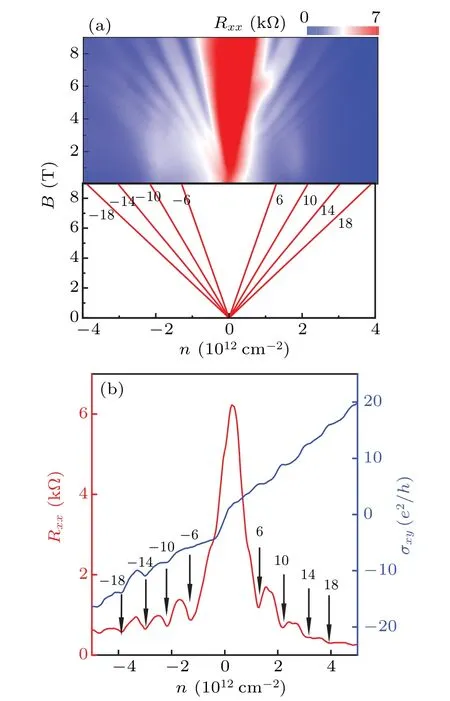
Lastly,we perform magnetic transport measurements for the TLG/hBN moir´e superlattice.In a strong perpendicular magnetic field,the two-dimensional electronic system in TLG obeys the Landau quantization and gives quantized Hall conductanceσxy=v×e2/h, wherevis the Landau level (LL)filling factor.In graphene multilayer systems, the number of graphene layers as well as the stacking order determines the characteristics of the Landau level spectrum.According to previous reports,the LLs in ABC trilayer graphene gives Hall plateaus at[32,38]σxy=±(ge2/h)(nLL+N/2)whereN=3 is the number of layers,nLLis the LL index,g=4 is the LL degeneracy accounting for spin and valley degrees of freedom,eis the electron charge,andhis Planck’s constant.By contrast,the LLs in ABA trilayer graphene can be viewed as a superposition ofdependent monolayerlike LLs andB-dependent bilayerlike LLs.[38,39]Figure 3(a) shows a color mapping of longitudinal resistance(Rxx)as a function of carrier density(n)and magnetic field(B),and the lower panel is a corresponding schematic highlighting the trajectories of the resistance minimum.We can observe a series of Landau fans from CNP that corresponds to the filling factorν=±6,±10,±14,...Figure 3(b) showsRxxand Hall conductanceσxyatB=9 T,from which near quantized Hall conductanceσxyandRxxminima are observed atν=±6,±10,±14,...Anyway, these magneto transport results do suggest that the epitaxial trilayer graphene has the characteristics of ABC stacking order.

Fig.3.Shubnikov–de Haas oscillations in our grown trilayer graphene.(a) Top longitudinal resistance Rxx as a function of carrier density n and magnetic field B.Bottom,the corresponding schematics that identifies visible Landau level fans.(b) Longitudinal resistance (Rxx, red)and Hall conductance(σxy,blue)versus carrier density n at T =1.8 K,B=9 T.
In conclusion,we successfully realized the epitaxy of trilayer graphene/hBN moir´e superlattices.The moir´e periodicity of∼15 nm is stable and uniform, formed due to the lattice mismatch between TLG and hBN with zero twisted angle.The electrical transport measurements in TLG/hBN suggest an ABC stacking order of TLG, supported by the evidences of gate-tunable band gap and Landau levels spectra.We also observed a resistance peak at 1/2 filling, indicating a strong correlation in the epitaxial ABC-TLG/hBN superlattice.Although more efforts are needed to address sample quality issues in future,our work indicates that epitaxy might provide a stable and reproducible new way to obtain moir´e superlattice for investigating strong correlated physics.
Acknowledgements
Project supported by the National Key Research and Development Program of China(Grant No.2020YFA0309600),the National Natural Science Foundation of China (Grant Nos.61888102, 11834017, and 12074413), the Strategic Priority Research Program of CAS (Grant Nos.XDB30000000 and XDB33000000), and the Key-Area Research and Development Program of Guangdong Province, China (Grant No.2020B0101340001).K.W.and T.T.acknowledge support from the Elemental Strategy Initiative conducted by the MEXT, Japan (Grant No.JPMXP0112101001), JSPS KAKENHI (Grant Nos.19H05790, 20H00354, and 21H05233),and A3 Foresight by JSPS.
- Chinese Physics B的其它文章
- First-principles calculations of high pressure and temperature properties of Fe7C3
- Monte Carlo calculation of the exposure of Chinese female astronauts to earth’s trapped radiation on board the Chinese Space Station
- Optimization of communication topology for persistent formation in case of communication faults
- Energy conversion materials for the space solar power station
- Stability of connected and automated vehicles platoon considering communications failures
- Lightweight and highly robust memristor-based hybrid neural networks for electroencephalogram signal processing

