SnP2S6 半导体层数依赖的压电效应
2023-04-29 15:28:19乔玲郭宇周思
四川大学学报(自然科学版) 2023年5期
乔玲 郭宇 周思


摘要: 二維压电材料在能源、电子和光电子学方面的应用引起了越来越多的关注. 从实验合成的压电晶体SnP 2 S 6 出发,我们系统研究了单层、双层、三层和块体SnP 2 S 6 的压电效应. 第一性原理计算表明:层状SnP 2 S 6 具有良好的热力学和动力稳定性,其带隙和载流子有效质量与层数无关,而压电性质具有明显的层数依赖性;单层SnP 2 S 6 的压电系数( d 11 )高达 14.18 pm/V ,远大于MoS 2 、 h -BN和InSe的压电系数,双层SnP 2 S 6 的面外压电系数( d 33 )大于12 pm/V. 优异的压电性能使SnP 2 S 6 在二维压电传感器和纳米发电机等器件中的应用成为可能.
关键词:二维材料; SnP 2 S 6 半导体; 压电性质; 电子结构; 层数
中图分类号: O469 文献标识码:A DOI:10.19907/j.0490-6756.2023.054001
收稿日期: 2023-04-07
基金项目: 国家自然科学基金(12004065, 12222403, 11974068); 中央高校基本科研业务费(DUT22ZD103, DUT22RC(3)009, DUT20LAB110); 辽宁省博士启动基金(2022-BS-081)
作者简介: 乔玲(1997-), 女, 硕士研究生, 研究方向为计算凝聚态物理. E-mail: qiaolingling@mail.dlut.edu.cn
通讯作者: 郭宇. E-mail: guoyu_dlut@dlut.edu.cn; 周思. E-mail: sizhou@dlut.edu.cn
Layer-dependent piezoelectric effect in SnP 2 S 6 semiconductor
QIAO Ling, GUO Yu, ZHOU Si
(Key Laboratory of Materials Modification by Laser, Ion and Electron Beams, Ministry of Education, College of Physics, Dalian University of Technology, Dalian 116024, China)
Piezoelectric two-dimensional (2D) materials draw growing interest for applications in energy harvesting, electronics and optoelectronics. Starting from the experimental synthesized piezoelectric SnP 2 S 6 crystal, we investigate the piezoelectric properties of monolayer, bilayer, trilayer and bulk SnP 2 S 6 by first-principles calculations. Layered SnP 2 S 6 is energetically, thermodynamically and dynamically stable. The bandgap and carrier effective mass of SnP 2 S 6 are independent on the number of layers, while the piezoelectric properties are layered dependent. Monolayer SnP 2 S 6 possesses piezoelectric coefficients ( d 11 ) up to 14.18 pm/V, much higher than the values of MoS 2 , h -BN and InSe monolayers. Bilayer SnP 2 S 6 has out-of-plane piezoelectric coefficients ( d 33 ) more than 12 pm/V. The prominent piezoelectric effect enables this novel 2D material for the applications of piezoelectric sensors and nanogenerators.
Two-dimensional materials; SnP 2 S 6 semiconductor; Piezoelectricity; Electronic structures; Layer-dependency
1 Introduction
Piezoelectric materials have a wide range of applications in systems that require robust electrical-mechanical coupling, which includes mechanical stress sensors, actuators, and energy harvesting devices [1-6] . Crystals based on the wurtzite structure are well-known piezoelectric materials, such as a-quartz (piezoelectric coefficient is 2.3 pm/V ), GaN (3.1 pm/V) and AlN (5.1 pm/V) , which are widely used in the piezotronic and piezo-phototronic devices [7-9] . However, the small piezoelectric coefficients of wurtzite semiconductors limit the mechanical-electrical energy conversion efficiency [8, 9] .
Recently, two-dimensional (2D) materials have sparked interest for the piezoelectric applications because of their high crystallinity and ability to withstand enormous strain [10-15] . Experimental studies have detected the piezoelectric signals in 2D materials, such as monolayer MoS 2 [16] , h -BN [17] and SnS 2 nanosheets [18] . The piezoelectric effect is inconspicuous, e.g., the measured piezoelectric polarization e 11 of monolayer MoS 2 is only around 2.9×10 -10 C/m [19] , and the mechanical-electrical energy conversion rate is limited to be about 5% [16] . Theoretical investigations predict that 2D piezoelectric materials, including group-III monochalcogenide [6, 20] , MoS 2 [21] and h -BN [21] monolayers, have normal piezoelectric coefficients below 10 pm/V. Therefore, finding flexible, stable, and efficient 2D piezoelectric materials is crucial.
Layered SnP 2 S 6 crystal has been synthesized by chemical transport reactions [22, 23] . The atomic structure of layered SnP 2 S 6 is presented in Fig.1, which exhibit non-centrosymmetry with D 3 and C 3 point groups for monolayer and bulk systems, respectively. Bulk SnP 2 S 6 is a semiconductor with a moderate indirect bandgap of 2.07 eV [24] . Moreover, it presents strong piezoelectric signals in the experiments [25, 26] . Correspondingly, the nonmonotonic pressure dependence of the structural polarization is observed. The ionic and electronic polarization for the SnP 2 S 6 crystal reaches maximum at ~2 GPa and ~65 GPa, respectively [27] . A strong piezoelectricity occurs in SnP 2 S 6 due to the following reasons: (1) their stable structures are non-centrosymmetric, allowing them to be piezoelectric; (2) their puckered symmetries are much more flexible, which can further enhance the piezoelectric effect. In view of the piezoelectricity in bulk SnP 2 S 6 , 2D SnP 2 S 6 would be excellent piezoelectric materials.
Herein, we systematically investigate the piezoelectric properties of layered SnP 2 S 6 that can be exfoliated from its layered bulk phase. The dynamic and thermal stabilities of layered SnP 2S 6 were assessed, and their electronic properties were explored by first-principles calculations. Importantly, these layered SnP 2 S 6 are potential piezoelectric materials with high piezoelectric coefficients up to 14.18 pm/V. This layered piezoelectric material represents a new class of nanomaterials for the next generation of ultra-sensitive mechanical detectors, energy conversion devices, and consumer-touch sensors.
2 Computational methods
Density functional theory calculations were performed by using the Vienna ab initio simulation package (VASP) [28, 29] , with the plane-wave basis set with an energy cutoff of 500 eV, the projector augmented wave potentials (PAW) [30] , and the generalized gradient approximation parameterized by Perdew, Burke and Ernzerhof (GGA-PBE) [31] for the exchange-correlation functional. The convergence criteria for total energy and residual force on each atom were set to be 10 -7 eV and 0.01 eV/, respectively. For unit cell of layered SnP 2 S 6 , the Brillouin zone was sampled with a Γ-centered 13 × 13 × 1 Monkhorst-Pack k-points grid. Note that the standard GGA functional underestimates band gaps; thus a hybrid functional (HSE06) [32] was also used to compute the electronic band structures of layered SnP 2 S 6 .
To examine the dynamic stability of layered SnP 2 S 6 , phonon dispersion was computed using the Phonopy code based on the density functional perturbation theory (DFPT) [33] incorporated with VASP. The ab initio molecular dynamics (AIMD) simulations [34] with the PAW method and PBE functional were carried out to assess thermal stabilities of layered SnP 2S 6 . In the AIMD simulations, the initial configuration of this monolayer with 3 × 3 × 1 supercell was annealed under several temperatures. Each AIMD simulation in the NVT ensemble ( i.e ., at constant number of particles, volume, and temperature) lasted for 10 ps with a time step of 1.0 fs, and the temperature was controlled by using the Noseé-Hoover method [35] .
3 Results and discussions
Due to the successful fabrication of layered SnP 2 S 6 materials [22] , the monolayer counterpart can be obtained by mechanical exfoliation [36] . As shown in Fig. 1a, bulk SnP 2 S 6 is a natural pseudo-two-dimensional crystal, possessing planar 2D networks of puckered hexagonal structures in the xy plane and vdW interlayer stacking along the z direction. Bulk and trilayer SnP 2 S 6 have an ABC stacking with each layer laterally shifted by [ -1/3, 1/3] in fractional coordinates with respect to the lower neighboring layer. For structural models of bilayer SnP 2S 6, the structure forms AB stacking sequences according to the lateral shift mentioned above. To explore the possibility of exfoliating monolayer from the bulk crystal, we calculate the interlayer cohesive energy E c as follows:
E c = ( E bulk - 3× E monolayer )/ n 0 (1)
where E bulk and E monolayer are the total energy of bulk and monolayer SnP 2 S 6 in the unit cell, respectively; n 0 is the total number of atoms in the unit cell for the bulk system. The calculated interlayer cohesive energy of layered SnP 2S 6 is -0.07 eV/atom, comparable to the values of phosphorene (-0.055 eV/atom) [37] , graphite and h -BN (both are around -0.065 eV/atom) [38] .
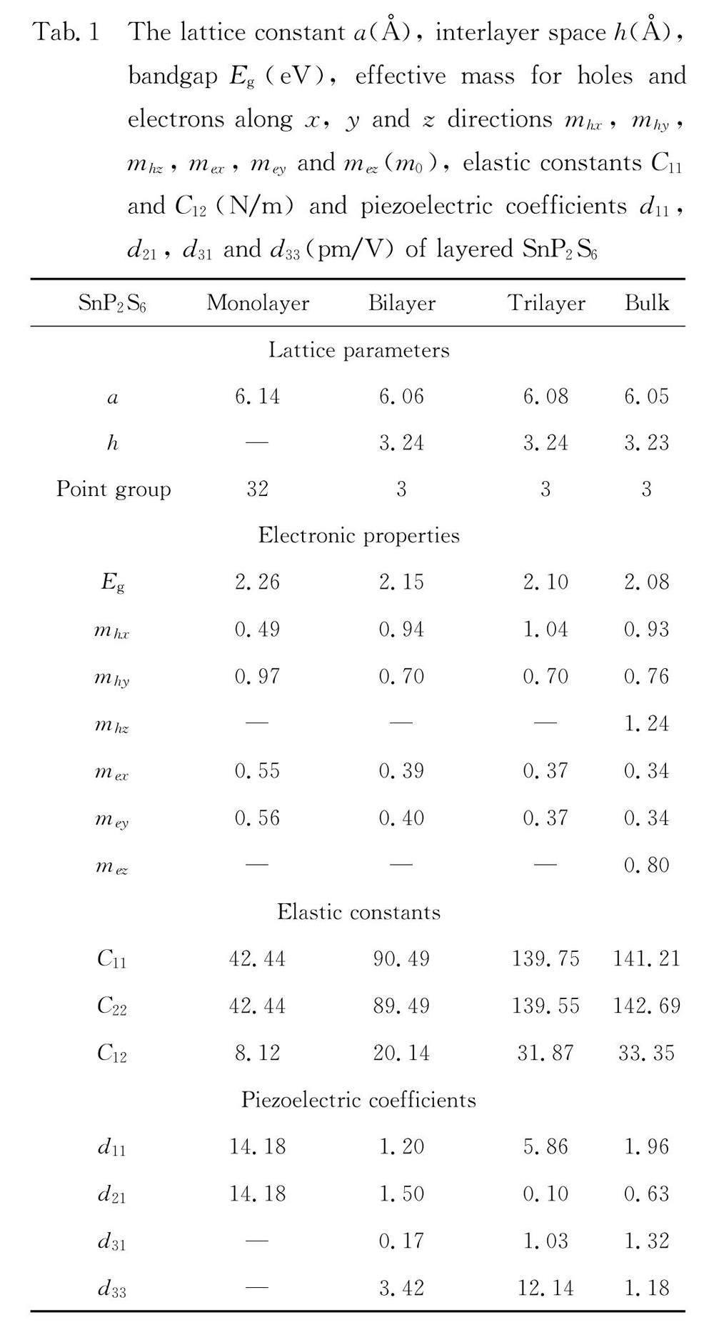
These results demonstrate the possible exfoliation of monolayer materials from the bulk solids. The unit cell of SnP 2 S 6 monolayer has one Sn, two P and six S atoms, with each Sn atom bonded with six S atoms, and each P atom bonded with three S atoms. As shown in Fig. 1, the optimized monolayer, bilayer, trilayer and bulk structure have a lattice constant ( a ) of 6.14, 6.06, 6.08 and 6.05 , respectively (see Tab. 1). Population analysis [39] reveals that SnP 2 S 6 monolayer is made of covalent bonds with bond order of 0.36 for Sn-S bonds and 0.54 for P-S bonds.
The stability of a 2D crystal is crucial for experimental fabrication and practical applications. To evaluate the energetic stability of SnP 2 S 6 monolayer, we first calculated the formation energy Δ H defined as
Δ H = ( E monolayer - n 1 × E 1 - n 2 × E 2 -
n 3 × E 3 )/ n (2)
where E monolayer is the total energy of SnP 2 S 6 monolayer, and E 1 , E 2 and E 3 is the energy per atom in Sn, P and S solids, respectively. The factors n 1 , n 2 and n 3 denote the number of Sn, P and S atoms in the unit cell, respectively, while the factor n represents the total number of atoms in the unit cell. The calculated Δ H is -0.27 eV/atom for monolayer SnP 2S 6, revealing that formation of SnP 2 S 6 monolayer is exothermic. The lattice dynamic stability of SnP 2 S 6 monolayer is assessed by calculating the phonon dispersion curves, as shown in Fig. 2a. No imaginary phonon mode is observed, indicating that SnP 2 S 6 monolayer is dynamically stable. We also performed AIMD simulations to examine the thermal stability of this 2D structure at 500 K. After 10 ps AIMD simulations, SnP 2 S 6 monolayer can maintain its structure above the room temperature (Fig. 2b).
Moreover, layered SnP 2 S 6 exhibits excellent electronic properties with moderate bandgaps. As shown in Fig. 3, monolayer, bilayer, trilayer and bulk SnP 2S 6 possess almost equal bandgap of 2.26, 2.15, 2.10 and 2.08 eV, respectively. The local density of states (LDOS) for these layered systems exhibit similar behavior: the edges of valence bands are dominated by the 3p orbitals of S atoms, while the conduction band edges stem mainly from the 5p orbitals of Sn atoms and 3p orbitals of S atoms. Meanwhile, the substantial overlap of LDOS near the Fermi level implies strong hybridization between the orbitals of Sn, P and S atoms. Overall, the electronic structures of layered SnP 2 S 6 are independent on the number of layers. As listed in Tab. 1, the computed carrier effective masses are in the range of 0.49~1.24 m 0 ( m 0 is the electron rest mass) for holes and 0.34~ 0.80 m 0 for electrons, respectively. Particularly, the effective masses for hole carriers could be as low as 0.34 m 0 along both x and y direction, indicating the carriers are rather mobile in these 2D sheets. Furthermore, layered SnP 2S 6 presents good optical absorption behavior. The optical absorption coefficients of monolayer, bilayer, trilayer and bulk SnP 2S 6 are obtained by computing the complex dielectric functions based on the HSE06 functional, as depicted in Fig. 4. They possess prominent optical absorption in ultraviolet regium with an absorption coefficient up to 10 5 cm -1 , suggesting that the layered SnP 2S 6 could be promising functional materials for ultraviolet detectors.
The SnP 2S 6 monolayer belong to 32 - point-group symmetry (No. 149), showing six independent elastic constants C ij and two independent piezoelectric polarization e ij [40] . Material constants of the SnP 2 S 6 monolayer is written in contracted notation as:
[C ij ]= C 11 C 12 C 13 C 14 0 0 C 12 C 11 C 13 -C 14 0 0 C 13 C 13 C 33 0 0 0 C 14 -C 14 0 C 44 0 0 0 0 0 0 C 44 C 14 0 0 0 0 C 14 C 66 (3)
[e ij ]= e 11 -e 11 0 e 14 0 0 0 0 0 0 -e 14 -e 11 0 0 0 0 0 0 (4)
Correspondingly, the piezoelectric coefficients can be obtained as follows:
[ d ij ] = [ e ij ][ C ij ] T-1 (5)
where [ C ij ] T-1 is the inverse of the transpose [ C ij ] T . For monolayer SnP 2 S 6 , we focus on the elastic constants C 11 and C 12 , and the piezoelectric coefficient d 11 . [ C ij ] is determined by performing six finite distortions of the lattice and deriving the elastic constants from the strain-stress relationship [41] . We then calculated [ e ij ] by DFPT [42, 43] . Finally, d 11 can be solved according to the formula (5).
The calculated elastic stiffness coefficient C 11 for SnP 2 S 6 monolayer is 42.44 N/m, and the corresponding C 12 is relatively lower at 8.12 N/m. The elastic stiffness coefficients are generally smaller than those of typical 2D materials, such as graphene ( C 11 = 358.1 and C 12 = 60.4 N/m ) [44] , MoS 2 ( C 11 = 130 and C 12 = 32 N/m) [21] , and InSe ( C 11 = 51 and C 12 = 12 N/m) [20] , demonstrating that the SnP 2 S 6 monolayer has a greater flexibility. The polarization tensor of the unit cell was obtained using the LEPSILON tag in VASP. The polarization vector of e 11 is 1.52×10 -10 C/m for SnP 2 S 6 monolayer, larger than the values of h -BN monolayer ( e 11 = 1.38×10 -10 C/m) [21] and InSe monolayer ( e 11 = 0.57×10 -10 C/m) [20] . According to the equation (5), the piezoelectric coefficients d 11 is calculated to be 14.18 pm/V, which is one or two orders of magnitude larger than the values of MoS 2 monolayer (3.74 pm/V) [21] , h -BN monolayer (0.60 pm/V) [20] and InSe monolayer (1.46 pm/V) [17] . The large piezoelectric coefficients indicate that SnP 2S 6 monolayer is suitable for 2D piezoelectric sensors and nanogenerators.
Then, we investigated the piezoelectric effects influenced by the number of layers. Bilayer, trilayer and bulk SnP 2S 6 hold 3-point-group symmetry with material constants as follows:
[C ij ]= C 11 C 12 C 13 C 14 -C 25 0 C 12 C 22 C 13 -C 14 C 25 0 C 13 C 13 C 33 0 0 0 C 14 -C 14 0 C 44 0 0 -C 25 C 25 0 0 C 44 C 14 0 0 0 C 25 C 14 C 66 (6)
[e ij ]= e 11 -e 11 0 e 14 e 15 e 22 -e 22 e 22 0 e 15 -e 14 -e 11 e 31 e 31 e 33 0 0 0 (7)
Similarly, we calculated elastic stiffness coefficients and piezoelectric coefficients based on equations (6)(7). As presented in Tab.1, elastic constants and piezoelectric effects are dependent on the number of layers. For the bilayer, trilayer and bulk systems, C 11 and C 22 are almost identical and increased with the layers in the range of 90~142 N/m, which are much higher that the values of monolayer (~42 N/m). C 12 is also layer-related constants with the values of 20~33 N/m, also larger than 8 N/m in SnP 2S 6 monolayer. The increased elastic coefficients suggest the enhanced stiffness of bilayer, trilayer and bulk SnP 2S 6 in comparison with that of monolayer.
Multilayer SnP 2S 6 also exhibit strong piezoelectric effect. Due to the reduced symmetry in the bilayer, trilayer and bulk systems, they hold more typical piezoelectric coefficients, including d 11 , d 21 , d 31 and d 33 , compared with one coefficient d 11 of SnP 2 S 6 monolayer. As listed in Tab.1 and Fig.5, bilayer, trilayer and bulk SnP 2S 6 have d 11 ( d 21 ) of 1.20 (1.50), 5.86 (0.10) and 1.96 (0.63) pm/V, respectively, smaller than 14.18 pm/V of monolayer SnP 2 S 6 . Multilayered systems suffer from the decreased polarization due to the in-plane depolarizing electrostatic field of adjacent layers. However, multilayer SnP 2S 6 generates excellent out-of-plane piezoelectric effects. Specifically, piezoelectric coefficient d 31 for the multilayer is in the range of 0.17~1.32 pm/V, which are close to the values of typical piezoelectric materials, i.e ., 1.9 pm/V for bulk AlN and 1.6 pm/V for bulk GaN. Moreover, the piezoelectric coefficient d 33 of trilayer SnP 2S 6 could be as high as 12.14 pm/V, much larger than 5.1 pm/V for bulk AlN and 2.6 pm/V for bulk GaN [7-9] . The appreciable out-of-plane piezoelectric effect would endow these SnP 2 S 6 systems with multiple functions for piezoelectric applications.
4 Conclusions
Motivated by the experimental fabricated SnP 2 S 6 crystal, we demonstrated the excellent electronic properties and superior piezoelectric effect of layered SnP 2 S 6 . Our first-principles calculations show that layered SnP 2 S 6 are energetically, dynamically and thermally stable. In particular, the bandgaps are about 2.20 eV and carrier effective mass of SnP 2 S 6 are in the range of 0.49~1.24 m 0 for holes and 0.34~0.80 m 0 for electrons, which are independent on the thickness. Moreover, SnP 2S 6 monolayer has large in-plane piezoelectric coefficients of 14.18 pm/V, significantly larger than those of common 2D materials, such as MoS 2 , h -BN and InSe. In addition, SnP 2S 6 bilayer yields out-of-plane piezoelectric coefficients up to 12 pm/V. As a remark, layered SnP 2 S 6 have been synthesized in experiment and the monolayer phase can be obtained by mechanical exfoliation. The enhanced piezoelectric effect and favorable semiconducting properties of this novel 2D material would advance the development of ultra-sensitive detectors, nanogenerators, low-power electronics, and nanoscale electromechanical systems.
References:
[1] Cui H, Hensleigh R, Yao D, et al . Three-dimensional printing of piezoelectric materials with designed anisotropy and directional response [J]. Nat Mater, 2019, 18: 234.
[2] Briscoe J, Dunn S. Piezoelectric nanogenerators-a review of nanostructured piezoelectric energy harvesters [J]. Nano Energy, 2015, 14: 15.
[3] Liu H, Zhong J, Lee C, et al . A comprehensive review on piezoelectric energy harvesting technology: materials, mechanisms, and applications [J]. Appl Phys Rev, 2018, 5: 041306.
[4] Covaci C, Gontean A. Piezoelectric energy harvesting solutions: a review [J]. Sensors, 2020, 20: 3512.
[5] Elahi H, Eugeni M, Gaudenzi P. A review on mechanisms for piezoelectric-based energy harvesters [J]. Energies, 2018, 11: 1850.
[6] Guo Y, Zhou S, Bai Y, et al . Enhanced piezoelectric effect in Janus group-III chalcogenide monolayers [J]. Appl Phys Lett, 2017, 110: 163102.
[7] Wang Z L. Progress in piezotronics and piezo-phototronics [J]. Adv Mater, 2012, 24: 4632.
[8] Bernardini F, Fiorentini V, Vanderbilt D. Polarization-based calculation of the dielectric tensor of polar crystals [J]. Phys Rev Lett, 1997, 79: 3958.
[9] Guy I L, Muensit S, Goldys E M. Extensional piezoelectric coefficients of gallium nitride and aluminum nitride [J]. Appl Phys Lett, 1999, 75: 4133.
[10] Li Y Y, Zhou B X, Zhang H W, et al . Doping-induced enhancement of crystallinity in polymeric carbon nitride nanosheets to improve their visible-light photocatalytic activity [J]. Nanoscale, 2019, 11: 6876.
[11] Lee J, Huang J, Sumpter B G, et al . Strain-engineered optoelectronic properties of 2D transition metal dichalcogenide lateral heterostructures [J]. 2D Mater, 2017, 4: 021016.
[12] Zhang Y, Jie W, Chen P, et al . Ferroelectric and piezoelectric effects on the optical process in advanced materials and devices [J]. Adv Mater, 2018, 30: 1707007.
[13] Zhou D R, Wang B. First-principles study on structure and properties of In 2(PS 3) 3 monolayer with a direct band-gap [J]. J At Mol Phys(原子与分子物理学报), 2023, 40: 036007. (in Chinese)
[14] Xiong J F, Sang B M, Li Q F, et al . First-principles study on the elastic and electronic properties of MgNi 2Bi 4 [J]. J At Mol Phys(原子与分子物理学报), 2022, 39: 056005. (in Chinese)
[15] Ding Y C, Yuan H, Xu M. First-principles study of lattice thermal conductivity of 2D Mo 2C [J]. J At Mol Phys(原子与分子物理学报), 2022, 39: 016007. (in Chinese)
[16] Wu W, Wang L, Li Y, et al . Piezoelectricity of single-atomic-layer MoS 2 for energy conversion and piezotronics [J]. Nature, 2014, 514: 470.
[17] Kuang H, Li Y, Huang S, et al . Piezoelectric boron nitride nanosheets for high performance energy harvesting devices [J]. Nano Energy, 2021, 80: 105561.
[18] Wang Y, Vu L M, Lu T, et al . Piezoelectric responses of mechanically exfoliated two-dimensional SnS 2 nanosheets [J]. ACS Appl Mater Inter, 2020, 12: 51662.
[19] Zhu H, Wang Y, Xiao J, et al . Observation of piezoelectricity in free-standing monolayer MoS 2 [J]. Nat Nanotechnol, 2015, 10: 151.
[20] Li W, Li J. Piezoelectricity in two-dimensional group-III monochalcogenides [J]. Nano Res, 2015, 8: 3796.
[21] Duerloo K A N, Ong M T, Reed E J. Intrinsic piezoelectricity in two-dimensional materials [J]. J Phys Chem Lett, 2012, 3: 2871.
[22] Wang Z, Willett R D, Laitinen R A, et al . Synthesis and crystal structure of SnP 2 S 6 [J]. Chem Mat, 1995, 7: 856.
[23] Zhang Y, Wang F, Feng X, et al . Inversion symmetry broken 2D SnP 2 S 6 with strong nonlinear optical response [J]. Nano Res, 2021.
[24] Jing Y, Zhou Z, Zhang J, et al . SnP 2 S 6 monolayer: a promising 2D semiconductor for photocatalytic water splitting [J]. Phys Chem Chem Phys, 2019, 21: 21064.
[25] Vysochanskii Y. Ferroelectricity in complex chalcogenides M′M″P 2 X 6 (M′, M″-Sn, Pb, Cu, In, Cr; X-S, Se) [J]. Ferroelectrics, 1998, 218: 275.
[26] Samulionis V, Banys J. Ultrasonic and piezoelectric studies of new layered ferroelectric compounds of Sn 2P 2S 6 family [J]. J Eur Ceram Soc, 2005, 25: 2543.
[27] Rushchanskii K Z, Vysochanskii Y M, Cajipe V B, et al . Influence of pressure on the structural, dynamical, and electronic properties of the SnP 2 S 6 layered crystal [J]. Phys Rev B, 2006, 73: 115115.
[28] Kresse G, Furthmüller J. Efficiency of ab-initio total energy calculations for metals and semiconductors using a plane-wave basis set [J]. Comput Mater Sci, 1996, 6: 15.
[29] Kresse G, Furthmüller J. Efficient iterative schemes for ab initio total-energy calculations using a plane-wave basis set [J]. Phys Rev B, 1996, 54: 11169.
[30] Blchl P E. Projector augmented-wave method [J]. Phys Rev B, 1994, 50: 17953.
[31] Perdew J P, Burke K, Ernzerhof M. Generalized gradient approximation made simple [J]. Phys Rev Lett, 1996, 77: 3865.
[32] Heyd J, Scuseria G E, Ernzerhof M. Hybrid functionals based on a screened Coulomb potential [J]. J Chem Phys, 2003, 118: 8207.
[33] Baroni S, De Gironcoli S, Dal Corso A, et al . Phonons and related crystal properties from density-functional perturbation theory [J]. Rev Mod Phys, 2001, 73: 515.
[34] Kresse G, Hafner J. Ab initio molecular dynamics for liquid metals [J]. Phys Rev B, 1993, 47: 558.
[35] Martyna G J, Klein M L, Tuckerman M. Nosé-Hoover chains: the canonical ensemble via continuous dynamics [J]. J Chem Phys,1992, 97: 2635.
[36] Novoselov K S, Geim A K, Morozov S V, et al . Electric field effect in atomically thin carbon films [J]. Science, 2004, 306: 666.
[37] Cai Y, Zhang G, Zhang Y W. Layer-dependent band alignment and work function of few-layer phosphorene [J]. Sci Rep, 2014, 4: 1.
[38] Graziano G, Klime J, Fernandez-Alonso F, et al . Improved description of soft layered materials with van der Waals density functional theory [J]. J Phys: Condens Matter, 2012, 24: 424216.
[39] Segall M D, Shah R, Pickard C J, et al . Population analysis of plane-wave electronic structure calculations of bulk materials [J]. Phys Rev B, 1996, 54: 16317.
[40] Ogi H, Ohmori T, Nakamura N, et al . Elastic, anelastic, and piezoelectric coefficients of α-quartz determined by resonance ultrasound spectroscopy [J]. J Appl Phys, 2006, 100: 053511.
[41] Le P Y, Saxe P. Symmetry-general least-squares extraction of elastic data for strained materials from ab initi o calculations of stress [J]. Phys Rev B, 2002, 65: 104104.
[42] Nakamura K, Higuchi S, Ohnuma T. Density functional perturbation theory to predict piezoelectric properties [M]∥Perturbation Methods with Applications in Science and Engineering. Rijeka: IntechOpen, 2018: 2.
[43] Gonze X, Lee C. Dynamical matrices, born effective charges, dielectric permittivity tensors, and interatomic force constants from density-functional perturbation theory [J]. Phys Rev B, 1997, 55: 10355.
[44] Andrew R C, Mapasha R E, Ukpong A M, et al . Mechanical properties of graphene and boronitrene [J]. Phys Rev B, 2012, 85: 125428.
猜你喜欢
科技创新与应用(2024年20期)2024-12-31 00:00:00
分子催化(2022年1期)2022-11-02 07:10:16
东北水利水电(2022年6期)2022-06-28 06:04:36
康复(2022年31期)2022-03-23 20:39:56
电子制作(2019年15期)2019-08-27 01:12:04
电子制作(2019年11期)2019-07-04 00:34:50
测控技术(2018年9期)2018-11-25 07:44:44
上海大中型电机(2017年4期)2017-02-06 05:26:59
科教导刊·电子版(2016年15期)2016-06-25 23:42:36
科教导刊·电子版(2016年5期)2016-04-19 08:11:10