Highly crystalline,highly stable n-type ultrathin crystalline films enabled by solution blending strategy toward organic single-crystal electronics
Yng Liu ,Shuyu Li ,Yihn Zhng ,Xioting Zhu ,Fngxu Yng,∗ ,Fei Jio,∗ ,Wenping Hu,b
a Tianjin Key Laboratory of Molecular Optoelectronic Sciences,Department of Chemistry,School of Science,Tianjin University,Tianjin 300072,China
b Haihe Laboratory of Sustainable Chemical Transformations,Tianjin 300192,China
Keywords:n-type organic field effect transistors Ultrathin film High-performance Composites
ABSTRACT The development of n-type semiconductor is still far behind that of p-type semiconductor on account of the challenges in enhancing carrier mobility and environmental stability.Herein,by blending with the polymers,n-type ultrathin crystalline thin film was successfully prepared by the method of meniscusguided coating.Remarkably,the n-type crystalline films exhibit ultrathin thickness as low as 5 nm and excellent mobility of 1.58 cm2 V−1 s−1,which is outstanding in currently reported organic n-type transistors.Moreover,the PS layer provides a high-quality interface with ultralow defect which has strong resistance to external interference with excellent long-term stability,paving the way for the application of n-type transistors in logic circuits.
Large area single crystal thin films are the best candidate materials for high-performance integrated plastic electronics,on account of the advantages of eliminating the interference of grain boundaries,defects,impurities and charge traps [1–4].Up to now,large area preparation of organic single crystal film has become a hot research field due to the inherent unique characteristics of organic molecules [5–7].On the one hand,they have good selfcrystallization and tend to aggregate crystallization in solution processing [8,9].On the other hand,because of the development of meniscus-guided coating (MGC) method,the orientation-inducing force can induce organic molecules to assemble in the same direction,enabling the formation of large-area highly crystalline films[10,11].For an organic field effect transistor (OFET),carrier transport channels are considered to be located within several molecular layers at the interface between the organic semiconductor and the insulating layer [12,13].At present,it has been reported that the monolayer molecular crystal can achieve the same performance as the bulk single crystal [14,15].Moreover,the ultrathin crystal film also has inherent incomparable unique advantages.On the one hand,the ultrathin feature can greatly reduce the bulk resistance of the semiconductor,facilitating the carrier injection[16,17].On the other hand,the carriers in the ultrathin channel can be efficiently regulated by the gate,and thus the carriers can be completely depleted in the depletion region to achieve ultra-low off-state current [18,19].Currently,the methods of preparing ultrathin single crystals mainly include liquid surface substrate method and the MGC method.Despite the liquid substrate method can prepare two-dimensional organic crystals with a controllable number of layers based on spatial confinement,it cannot be fabricated on a large scale [20].By contrast,the MGC method can be fabricated in a large area.However,in order to ensure the continuity of the film,the thickness of the film is often increased,resulting in a challenge of achieving ultrathin thickness.Although there are a few reports on p-type ultrathin single crystal films [21],investigation on largearea n-type ultrathin crystalline films is scarce.
In addition,the long-term storage and operational stability of n-type ultrathin semiconductor films is another formidable challenge that needs to be addressed.There are two main reasons for the morphological evolution of organic thin films after long-term storage.Firstly,molecular films are assembled by weak van der Waals interactions between organic molecules [22,23].Secondly,the heterointerface is generally accompanied by the existence of interfacial stress [24].Moreover,this phenomenon will be more pronounced for ultrathin films.To overcome this problem,it has been reported that increasing the thickness of the film can improve the stability [25,26].Even worse,the stability of n-type semiconductor thin films is a long-term problem in the field,mainly because the electronic properties of organic semiconductors are easily affected by water and oxygen [27,28].Thus,the stability of n-type ultrathin films will be a huge challenge,which needs to be solved by developing sophisticated strategies.
Herein,we develop a polymer blending strategy to realize the preparation of n-type ultrathin films,obtaining high-performance n-type organic field effect transistors with excellent stability.Choosing 4,4'-(2λ4δ2-benzo[1,2-c:4,5-c’]bis[1,2,5]thiadiazole-4,8-diyldi-5,2-thiophenediyl)bis[2-dodecylbenzonitrile] (TU-3) as the n-type semiconductor,we obtained n-type ultrathin films owing to the properties of the continuous film formation and efficient crystallization of the polymer polystyrene (PS) in TU-3/PS composite.The electron mobility of the corresponding device is as high as 1.58 cm2V−1s−1,which is the highest value for n-type ultrathin films.More importantly,the n-type ultrathin film achieves good long-term stability due to the addition of PS to stabilize the heterointerfacial stress,and the low defect system also enables the film to obtain good resistance to external interference.This study lays a solid foundation for the development of high-performance n-type ultrathin films for large area integrated electronics.
For the solution shearing method,ultra-low solution concentration or fast shear rate are generally required to prepare ultrathin films [29].Small molecules are not easy to form films due to their low viscosity,so we tend to increase the shear rate to reduce the thickness of the film,which often results in discontinuity and inhomogeneity of the film [10].However,the addition of polymers can significantly increase the viscosity and improve the wettability of the solution,thereby improving the growth kinetics,which is more favorable for the growth of thin films [30,31].In terms of molecular selection,we chose small molecule TU-3 and polymer PS with good solubility and high stability [32,33].In film preparation,we chose the strategy of polymer blending to assist solution shearing (Fig.1a).By using the method of meniscus-guided coating,an orientation force is applied to small molecules to induce crystallization toward the dominant direction.The uniform solidification of PS with long-chain structure at the bottom layer provides a favorable platform for the deposition of TU-3 small molecules,thereby obtaining continuous and uniform ultrathin films by adjusting the appropriate shear rate (Fig.1b).Optical micrographs reveal ultrathin films with centimeter-scale dimensions and smooth,flat surfaces,and atomic force microscopy (AFM) images indicate a thickness of 5.5 nm (Fig.S1 in Supporting information).The microstructure of the ultrathin film is revealed by AFM,and it is found that the blend film has a more continuous and flatter surface than the single-component film,and the root mean square roughness (RMS) is reduced from 1.49 nm to 0.48 nm due to the introduction of polymers,which reflects that the blending strategy improves the uniformity and continuity of the ultrathin films (Figs.1c and d).In order to further analyze the crystallinity and structure of the ultrathin film,it is first observed under a polarizing microscope (POM).When the polarization angle is rotated by 45°,the film shows a uniform color change and a significant extinction phenomenon,indicating that it has a long-range ordered internal structure (Figs.1e and f).Meanwhile,the out-of-plane X-ray diffraction pattern shows that the blend film had sharper diffraction peaks,indicating that the introduction of PS effectively improves the crystallinity of TU-3 (Fig.S2 in Supporting information).Besides,the selected-area electron diffraction (SAED) image shows that the ultrathin film has periodically arranged diffraction spots,further proving its single-crystal structure (Fig.1g).
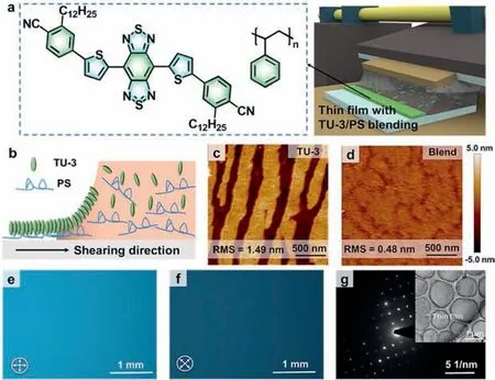
Fig.1. (a) Chemical structure of TU-3 and PS and schematic diagram of ultrathin film preparation.(b) Schematic diagram of small molecule deposition process.(c,d) AFM images of a pure TU-3 film and a TU-3/PS blend ultrathin film on Si/SiO2 substrate.(e,f) POM images of an ultrathin film.(g) An SAED image of an ultrathin film.Inset: a transmission electron microscope image (TEM) of the ultrathin film.
We transferred Ag (80 nm)/Au (80 nm) as source and drain electrodes on the ultrathin films,and constructed bottom-gate topcontact (BGTC) OFETs to study its electrical properties (Fig.2a and Fig.S3 in Supporting information).All experiments were performed at room temperature and in air environment.The transfer characteristic curves of ultrathin film-based OFETs are shown in Fig.2b,and the corresponding output curves are shown in Fig.2c.An electron mobility of 1.58 cm2V−1s−1is obtained under optimal conditions with an on-off ratio greater than 107.Moreover,we systematically studied the effect of different annealing temperatures on the mobility,and found that the mobility of the device was the highest when annealing at 100°C for 1 h (Fig.2d),which is attributed to the volatilization of impurities such as organic solvents and water in the ultra-thin film,as well as the enhancement of film crystallinity (Fig.S4 in Supporting information).In addition,the effect of different mixing ratios on the mobility is also crucial,and the performance of the device is the best when the mixing ratio is 3:1 (Fig.S5 in Supporting information).It is worth mentioning that with the increase of shear rate,the thickness of the film will decrease inversely proportional,and the thickness of the ultra-thin film can be as low as 5 nm.When the shear rate is 0.25 mm/s,the mobility of the ultrathin films reaches the maximum value.However,continuing to increase the shear rate significantly increases the defects of the film,thereby reducing its electrical transport capacity (Fig.2e and Fig.S6 in Supporting information).The mobilities of 30 devices under the optimal conditions are counted as shown in Fig.2f,which is a normal distribution.The average electron mobility is 1.09 cm2V−1s−1,and the maximum electron mobility is 1.58 cm2V−1s−1,which is the highest value reported so far in OFETs used TU-3 as the n-type semiconductor.
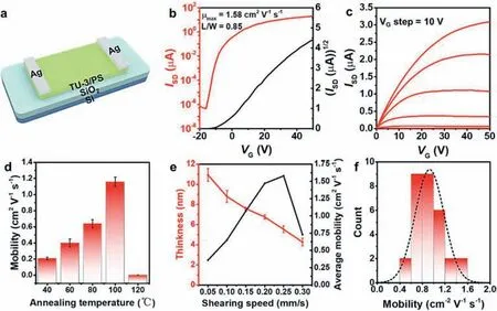
Fig.2. (a) Schematic diagram of OFET device based on ultrathin films.Representative transfer (b) and output (c) curves of OFETs based on ultrathin films.(d) OFET mobility as a function of annealing temperature,the error bars were calculated from the standard deviations over 10 devices in each annealing temperature.(e) Film thickness and average mobility at different shear rates,the error bars were calculated from the standard deviations over 5 devices at each shear rate.(f) Histogram of mobility distribution of 30 devices,with average value of 1.09 cm2 V−1 s−1.
Long-term operational stability and environmental stability are one of the most important application metrics for n-type organic field effect transistors.We measured the output current of the device under a constant gate voltage of 20 V,and found that the device prepared based on the blending strategy showed better stability than the single-component device.After 8.5 h of continuous bias operation,the output current of the device still did not decay(Fig.3a).At the same time,the device was switched on and off 20 times within 2 h,and its transfer curve did not change distinctly(Fig.S7 in Supporting information).In order to explore its intrinsic mechanism,we tested the UV–vis absorption spectrum of the ultrathin film within six months,and the curve basically did not change,proving its good chemical stability (Fig.3b).The devices were then tested for photostability,and the OFETs exhibited good photostability to all wavelengths of light,which was attributed to the high molecular order in the conducting channel and the highquality interface between the dielectric layer and the semiconductor (Figs.3c-e) [34].It is worth noting that when the incident light is 365 nm,the off current of the device significantly increases,which is due to the generation of a large number of photo generated charge carriers in the active layer.However,the threshold voltage did not significantly shift,because there were few defects in the system and almost no hole trapping occurred,demonstrating the photostability of the transistor (Fig.3c).In the blend film,there is a more favorable enthalpy interaction between PS and SiO2,PS will preferentially deposit on the SiO2substrate [35,36],while the more hydrophobic TU-3 small molecules crystallize at the interface of air and film,which can be confirmed in scanning electron micrographs (SEM,as shown in Fig.3i).We also used X-ray photoelectron spectroscopy (XPS) to analyze the atomic ratios of C/S and C/N on the surfaces of blend and single-component films,and the phase separation result was confirmed by their equality (Fig.3j and Fig.S8 in Supporting information).Actually,PS layer passivates the electron traps on the surface of SiO2,provides a high-quality interface,and the whole system is a low-defect system with strong resistance to external interference,thus obtaining perfect stability (Figs.3k and l).Subsequently,we stored the device in air and tracked its mobility and threshold voltage over time.The introduction of PS also significantly improved the environmental stability of the device,and the change in threshold voltage after 9 months was only about 5 V (Fig.3f).Moreover,the mobility of the device is only reduced by about 10% after 4 months of storage.After 8 months,the mobility of the device can still be as high as 1 cm2V−1s−1(Fig.3g).Compared with the previously reported stability of n-type OFETs [37–46],our work is at the cutting edge (Fig.3h).
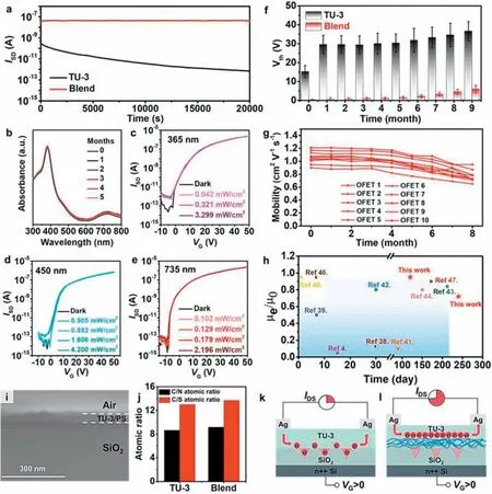
Fig.3. (a) The I-t curves of OFETs based on single-component and blend ultrathin films under applied constant voltage VG of 20 V at VD of 40 V.(b) Time-dependent UV–vis spectra of a blend ultrathin film under ambient air.Transfer curves of OFETs based on blend ultrathin films in dark and under different illumination intensities at (c)365 nm,(d) 450 nm and (e) 735 nm.(f) Time-dependent threshold voltage shift of single-component and blend OFETs stored in air at room temperature,the error bars were calculated from the standard deviations over 10 devices.(g) Time-dependent electron mobility of 10 OFETs based on blend ultrathin films stored in air at room temperature.(h) Comparison of n-type OFET stability.(i) Cross-sectional SEM image of a blend ultrathin film.(j) Atomic ratios of the surfaces of single-component and blend ultrathin films.(k,l) The possible mechanism for the stability of ultrathin films.
To demonstrate the universality of this strategy for different substrates,a high-quality alumina dielectric layer was prepared by template stripping method [47],and then grew a blend ultrathin film on the dielectric (Fig.S9 in Supporting information).Optical microscope and polarized optical microscope images prove that the thin film has a flat surface and good crystallinity (Figs.4ac).Moreover,the morphology and thickness of the thin film did not significantly change with the substrate (Fig.S10 in Supporting information).Subsequently,we thermally evaporated 2 nm 2,3,5,6-tetrafluoro-7,7,8,8-tetracyanoquinodimethane (F4-TCNQ) as a buffer layer,and then deposited 30 nm Ag as the top electrode to prepare a large-area transistor array (Fig.S11 in Supporting information),and the schematic diagram of the devices structure is shown in Fig.4d.Figs.4e and f show the transfer and output curves of the devices,respectively.The highest mobility can reach 0.53 cm2V−1s−1,which is one of the best performance n-type low voltage transistors at present (Table S2 in Supporting information).The mobility of 6× 6 transistors is counted,and it has a relatively uniform distribution (Fig.4i).Likewise,low-voltage devices exhibit good operational stability and environmental stability (Figs.4g and h),which provides a favorable guarantee for the development of organic logic circuits in the future.
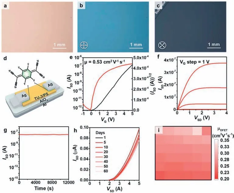
Fig.4. (a) OM and (b,c) POM images of an ultrathin film on Al/AlOx substrate.(d) Schematic diagram of low-voltage transistors based on ultrathin films.(e) Representative transfer and (f) output curves of OFETs based on ultrathin films.(g) The I-t curve of OFETs under applied constant voltage VG of 2 V at VD of 4 V.(h) Time-dependent I-V curves of OFETs under ambient air.(i) The distribution of OFET mobilities of a 6× 6 low-voltage transistor array.
In conclusion,we have fabricated large-area ultrathin n-type crystalline filmsviausing the polymer blending strategy.Through the introduction of the polymer and the regulation of the shear rate,the electron mobility of the ultrathin film can be as high as 1.58 cm2V−1s−1when the thickness can be as low as 5.5 nm.In the blend system,the favorable interaction between PS and TU-3 molecules regulates the arrangement of TU-3 molecules,enhances the crystallinity of the film,and thus improves the electrical transport performance of the device.Moreover,PS solves the instability caused by n-type semiconductors and ultrathin film,and the lowdefect system also enables the film to obtain good resistance to external interference.Finally,we have successfully fabricated n-type OFETs with high stability and high performance,while low-voltage devices have good uniformity and stability,which has guiding significance for the development of logic circuits.
Declaration of competing interest
The authors declare that they have no known competing financial interests or personal relationships that could have appeared to influence the work reported in this paper.
Acknowledgments
The authors are grateful to the financial support of the National Key Research and Development Program (No.2022YFF1202700),National Natural Science Foundation of China (No.52121002) and the Haihe Laboratory of Sustainable Chemical Transformations.
Supplementary materials
Supplementary material associated with this article can be found,in the online version,at doi:10.1016/j.cclet.2023.108764.
 Chinese Chemical Letters2023年12期
- Chinese Chemical Letters的其它文章
- Spin switching in corrole radical complex
- Benzothiadiazole-based materials for organic solar cells
- Mono-functionalized pillar[n]arenes: Syntheses,host–guest properties and applications✰
- Recent advances in two-step energy transfer light-harvesting systems driven by non-covalent self-assembly✩
- From oxygenated monomers to well-defined low-carbon polymers
- Doping-induced charge transfer in conductive polymers
