Enhancing terahertz photonic spin Hall effect via optical Tamm state and the sensing application
Jie Cheng(程杰) Jiahao Xu(徐家豪) Yinjie Xiang(项寅杰) Shengli Liu(刘胜利)Fengfeng Chi(迟逢逢) Bin Li(李斌) and Peng Dong(董鹏)
1School of Science,New Energy Technology Engineering Laboratory of Jiangsu Province,Nanjing University of Posts and Telecommunications,Nanjing 210023,China
2College of Electronic and Optical Engineering&College of Flexible Electronics(Future Technology),Nanjing University of Posts and Telecommunications,Nanjing 210023,China
3School of Electrical Engineering,Nanjing Vocational University of Industry Technology,Nanjing 210023,China
Keywords: photonic spin Hall effect,optical Tamm state,InSb,gas sensor
1. Introduction
It is well known that left- and right-handed circularly polarized components can split transversely perpendicular to the incident plane when a linearly polarized beam propagates through inhomogeneous media, due to spin–orbit interaction of photons. This phenomenon is called the photonic spin Hall effect (PSHE), and it was firstly proposed by Onodaet al.in 2004.[1–3]PSHE can be considered as an optical version of spin Hall effect in electronic systems,where the roles of spin electrons and electric potential are replaced by spin photons and refractive index gradient, respectively.[1,2]Owing to its physical interest and potential applications in precision metrology, quantum information, and optical devices,PSHE has drawn significant attentions since its discovery.Until now,the reported applications of PSHE have covered various fields,such as biosensing,[4]real-time detection of chemical reaction rates,[5]and one-dimensional edge detection.[6]However,PSHE is generally a tiny phenomenon with the corresponding spin shift of only subwavelength scale, which seriously hinders its widespread applications. Several proposals have been put forward to enhance PSHE,based on the Brewster angle,[7]surface plasmon resonance (SPR),[8]inhomogeneous metamaterials,[9]and so on.[10–12]Nevertheless, the enhancement and dynamical modulation of PSHE remain an open challenge,highly desirable for its importance in modern optics.
The optical Tamm state (OTS), a new kind of surface wave confined at the interface between two different media,is an optical analogue of electronic Tamm state at crystal boundaries.[13]The OTS manifests itself as a narrow resonance in the optical transmittance or reflectance spectrum inside the bandgap. In contrast to conventional surface waves such as surface plasmon polaritons, OTS can be excited directly by both the TE and TM polarizations without special incident angles.[14–16]Due to these favorable characteristics,the potential applications of OTS have been explored in such uses as solar cells,[17]polariton laser,[18]optical resonators,[19]and large Goos–H¨anchen shift.[20]In recent years, OTS attracted increasing interests and offered an alternative platform to enhance the PSHE.The metal-distributed Bragg reflector(DBR)structure and one-dimensional photonic crystal heterostructure are typical systems for exciting the OTSs.[14,21,22]However,this traditional metal-DBR structure is unsuitable to excite the OTS in terahertz(THz)band.[23]Considering the progress of THz wave source and the outstanding applications in information and communications, biomedical imaging, and nondestructive evaluation and security, research of OTS-induced PSHE in THz range is of significant importance.
Looking for suitable materials instead of metals to excite THz OTS is the first and most urgent challenge. InSb is a narrow bandgap semiconductor with an electronic bandgap of 0.17 eV at 300 K,whose permittivity in THz range is similar to those of metals in visible region.[24]Previous reports have investigated the enhancement and adjustment of PSHE in THz range for InSb-based structure,therefore,InSb can be considered as a good candidate to explore the PSHE in THz range.[25]Here,by replacing the metal film in conventional metal-DBR structure with a semiconductor of InSb, a new type of InSb-DBR system is constructed. Moreover, the permittivity of InSb can be dynamically modulated by temperature,[26]which provides a new degree of freedom to manipulate the THz OTS and also PSHE behavior of InSb-DBR structure. The results show that the maximum spin shift of PSHE is up to 11.15 mm at optimal structural parameters and temperature, due to the strong excitation of THz OTS. The spin shift is very sensitive to the refractive index change of gas,therefore,a THz gas sensing device based on the enhanced PSHE via the excited OTS of this InSb-DBR structure is proposed with a superior intensity sensitivity of 5.873×104mm/RIU.
2. Theory and model
The InSb-DBR structure composed of InSb, the epsilonnear-zero material(ENZ)layer and the one-dimensional photonic crystal(1D-PC)is shown in Fig.1(a). InSb with the refractive index ofn2is placed on the surface layer of structure,and the thickness is defined asd2. The ENZ layer(n3=0.1)with the thickness ofd3is sandwiched between InSb and 1DPC.The lower part of space layer is followed by a 1D-PC consisting of 20 cycles of DBR. The DBR is composed of two kinds of media layers(A and B)with the thicknesses ofd4andd5, respectively. The refractive indices of media A and B aren4=1.9 andn5=2.25 in the THz band, respectively. The thicknesses of A and B are given byd4,5=λc/4n4,5, where the central wavelength is chosen asλc=270µm(i.e.,the central frequency offc=1.11 THz). The permittivity of InSb at THz frequencies can be obtained from the Drude model as follows:[27]

The Gaussian beam is incident on the surface InSb layer with an incident angleθi, as shown in Fig.1, and the PSHE of reflected light appears leading to the splitting of left-and righthanded circularly polarized components in they-axis direction. From the angular spectrum theory,the incident Gaussian beam can be expressed as
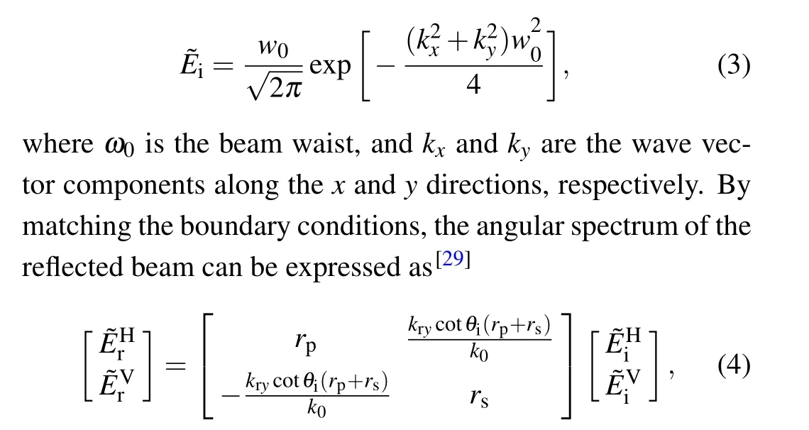
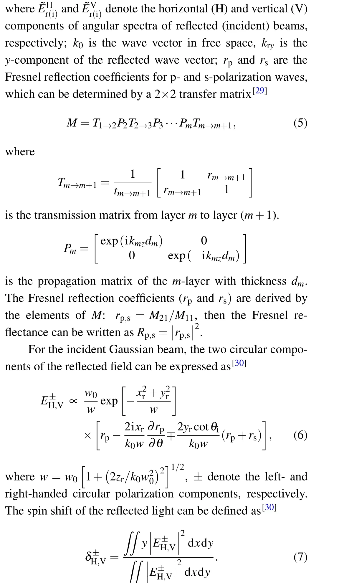
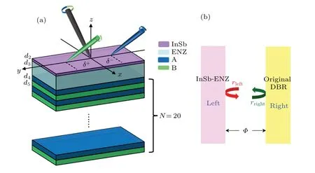
Fig.1. (a)Schematic diagram of the proposed InSb-DBR structure and the corresponding PSHE of reflected light. (b)A dissymmetric cavity,enclosed by the InSb-ENZ layer and a DBR.
3. Simulation results and analysis
In order to investigate the OTS-induced PSHE behavior of the InSb-DBR structure,we have to demonstrate the excitation of OTS by the proposed InSb-DBR structure in the THz region.Figure 2 displays the reflectance spectrum versus the frequency of incident light for TM polarization (p-polarization)and TE polarization(s-polarization).It can be clearly seen that there exists a photonic bandgap for the original DBR (without the addition of InSb and ENZ material) in the frequency range of 1.07–1.15 THz, in which the reflectance is nearly 1.For the InSb-DBR structure,a pronounced reflection dip in the bandgap region is observed under both TM and TE polarizations.This reflectance dip is deep and relatively narrow,which may be associated with the excitation of OTS.Compared with the condition of TE polarization,TM polarization wave excites a deeper reflection valley,almost reaching 0.Therefore,we set the central frequency of incident light as 1.11 THz,which corresponds to the reflectance dip of TM polarization.
It is known that excitation of OTS should satisfy the condition ofrleftrrightexp(2iΦ) = 1. As seen in Fig. 1(b), our InSb-DBR structure can be regarded as a dissymmetric cavity, enclosed by the InSb-ENZ layer on one side and a DBR on the other. Here,rleftandrrightrepresent the reflection coefficient of the incident electromagnetic waves on the InSb-ENZ layer and on the DBR,respectively,andΦis the phase change of the electromagnetic wave propagating in the cavity between two interfaces.[13,14,31]Using the transfer matrix method, the reflection coefficients on the interface of the InSb and DBR can be calculated. They arerleft=−0.9867−0.1474i andrright=−0.5577+0.8255i(TM polarization),rleft=0.9322−0.3280i,andrright=−0.5522+0.8297i(TE polarization),respectively. The above values perfectly satisfy the excitation condition of OTS, thus the narrow reflection valleys for TM and TE polarization in Fig. 2 are owing to the OTS of the InSb-DBR structure,which will result in the enhancing PSHE of reflected light.

Fig.2. The reflectance spectrum of the InSb-DBR structure versus the incident frequency for TM and TE polarizations. Here, the structural parameters are T =300 K,d2=35 nm and d3=400µm. The dashed line is the bandgap of original DBR structure.
Through our calculation,the excitation of OTS for InSb-DBR structure needs to meet the following structural requirements simultaneously: (i) The thickness of ENZ layer is greater than 300µm.(ii)The InSb thickness ranges from 1 nm to 10µm. However,the strength of OTS(i.e.,the value of reflection valley)is extremely sensitive to the thickness of InSb and ENZ layers. It is generally accepted that the spin shift of reflected light can be enhanced by enlarging the differences of Fresnel reflection coefficients betweenrsandrp. The giantδHprefers to have a smallrp, and largeδVwantsrsas small as possible.[8,32]Therefore, the thicknesses of InSb and ENZ layers affect the strength of OTS and then the PSHE behavior of reflected light for InSb-DBR structure. Figure 3 shows the Fresnel reflectance spectrum versus the incident angle with different thicknesses of ENZ and InSb layers. As shown in Fig. 3(a), by fixing the ENZ thickness (d3) to 400 µm, we found the prominent characteristic of OTS when the thickness of InSb layer(d2)changes from 5 to 70 nm. An increasedd2has little effect on the incident angle of OTS,but the penetration depth of OTS accordingly changes. The corresponding minimum value of reflectanceRpfor the InSb-DBR structure with differentd2is illustrated in Table 1. With the increment ofd2,Rpfirstly decreases to a small value and then continuously increases. The minimumRpof 1.50×10⁻⁷is obtained whend2=35 nm. UnlikeRp,Rsbecomes unchanged with increasing the incident angle from 10.1◦to 10.6◦,and it always maintains a large value(∼0.9)with differentd2.Similarly,the effect of ENZ thickness(d3)on theRpwithd2=35 nm is also shown in Fig.3(c).When the thickness of ENZ layer increases from 350µm to 450µm,the incident angle of OTS moves towards a smaller angle,accompanied by the varied penetration depth.

Fig. 3. Impact of thicknesses of the InSb layer (d2) on the reflectance(a) Rp and (b) Rs with d3 =400 µm. (c) The Rp curves for different thicknesses of the ENZ layer(d3),d2=35 nm. Here,T =300 K.
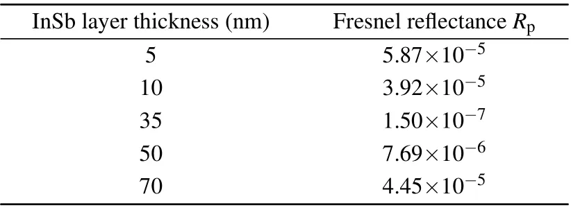
Table 1. The minimum values of Rp with different InSb thicknesses in Fig.3(a).
Therefore, for the InSb-DBR structure,Rpgets a nearzero value due to the strong excitation of OTS,whileRskeeps a large value (∼0.9) in the incident angle range from 10.1◦to 10.6◦. Considering the intimate relationship between the PSHE and Fresnel reflectance, the excitation of OTS would lead to a large ratio ofrs/rpand the resulting giant spin shiftδHof reflected light for the InSb-DBR structure. Note that the spin shifts for left-and right-circularly polarized light are the same in magnitude but opposite in signs. For simplicity,only the spin shift of left-circularly polarized component is plotted in the figures of next sections.
Figure 4 describes the role of InSb/ENZ thickness and the incident angle in PSHE of reflected light for the InSb-DBR structure. From Fig. 4(a), the value ofδ+His positive with small thickness of the InSb layer(d2)and incident angle,and then it reaches the positive peak in the spectrum of spin shifts as the InSb thickness increases to 35 nm, which is due to the strong excitation of OTS and the resultant near-zerorp.The sign of spin shifts changes from positive to negative,and then it exhibits the negative valley with the further increase ofd2and incident angle. Such variation can be attributed to the changed sign of the phaseϕpof Fresnel reflection coefficientrp. Meanwhile, the relationship between spin shiftδ+Hand the thickness of ENZ layer in Fig. 4(b) is similar to the condition of InSb thickness. Therefore, the spin shiftδ+Hof InSb-DBR structure changes with the incident angle and the InSb/ENZ thickness, and there are optimal parameters with the InSb/ENZ thickness to achieve the notable PSHE. The spin shiftδ+Hreaches up to 4.55 mm under the parameters ofd2=35 nm andd3=400µm, which can be attributed to the strong excitation of OTS in the InSb-DBR structure.
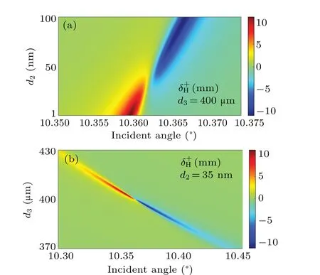
Fig.4. The dependences of spin shift δ+H (a)on d2 and incident angle with d3=400µm and(b)on d3 and incident angle with d2=35 nm.
InSb is a temperature-sensitive material, therefore, temperature can be an additional factor to modulate the behavior of PHSE in the InSb-DBR structure. Figure 5(a) shows the permittivity of InSb as a function of temperature. It can be clearly seen that both the real and imaginary parts of InSb permittivity stabilize to be a tiny value when temperature is lower than 250 K.With the continuous increase of temperature, the real component of InSb permittivity becomes negative, while the imaginary one increases to be a large positive value. The effect of temperature on the corresponding spin shiftδ+Hfor InSb-DBR structure is displayed in Fig. 5(b). It is demonstrated that the spin shiftδ+Hand the related excitation angle of OTS change slightly at low temperature, owing to the stable behavior of InSb permittivity. The giant spin shift is about 11.15 mm,about 6 times larger than the spin shift induced by InSb-supported long-range SPR for the incident frequency of 1 THz.[33]Then the spin shift undergoes a sign transformation with increasing temperature.Meanwhile,the magnitude ofδ+Hbecomes decreased,accompanied by the increment of OTS excitation angle.Consequently,temperature can be a new degree of freedom to flexibly tune the spin shift of PSHE for the InSb-DBR structure. Moreover, the optimal incident angle should be accordingly changed to excite the notable OTS and prominent spin shifts in future applications of PSHE-based devices.
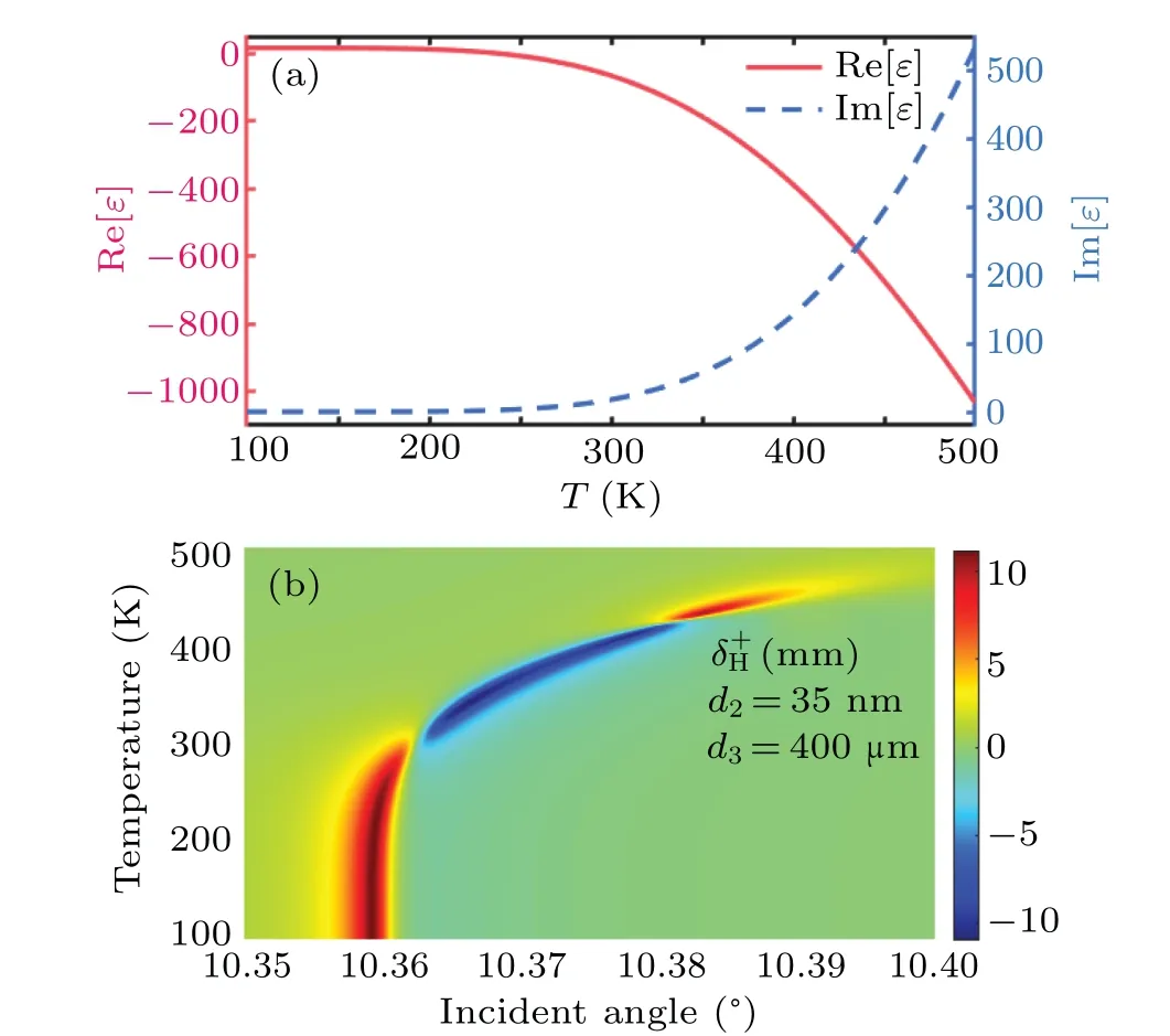
Fig. 5. (a) The permittivity of InSb (ε) for different temperatures. (b)The spin shift of δ+H versus temperature T and incident angle. Here d2=35 nm and d3=400µm.
Given the advantages of precise real-time detection and fast response,optical refractive index sensors have received a great deal of attention in potential applications including toxic monitoring, medical diagnose, food safety inspection, and so on.[4,34,35]Nowadays, most of the typical sensors are based on the SPR or resonant optical tunneling effect,and the sensing mechanisms are directly associated with the changes of reflection valley for different analytes. As a novel optical effect, PSHE opens the possibility for developing a new type of optical sensors. Compared with other traditional sensors,PSHE-based refractive index sensors exhibit the desirable accuracy and higher signal-to-noise ratio.[36]Until now, most optical sensors based on PSHE have been focused in the visible region,and the research of THz gas sensor is of significant importance, because the vibrational and rotational energy of most gas molecules lie in THz ranges. Here we replaced the first air layer of the InSb-DBR structure (in Fig. 1(a)) by the gas to be detected,and proposed a THz gas sensor based on the OTS-induced PSHE of the InSb-DBR system.Considering the intimate relationship between the PSHE and refractive index of analyte, when two different sensing analytes are detected,the corresponding spin shift will be distinctive. According to the intensity-based shift sensing scheme, the intensity sensitivity of PSHE sensors can be expressed asSδ+H=∆δ+H/∆n,
where ∆δ+His the variation of spin shift at a fixed working angle as shown in Fig.6,and ∆nis the refractive index difference of gas. We found that the spin shift is extremely sensitive to the refractive index change of detected gas, and the intensity sensitivity can be up to 5.873×104mm/RIU. This value is about two orders of magnitude greater than that of PSHE sensor based on InSb-supported long-range SPR.[33]Compared with the conventional micro-electromechanical system(MEMS) gas sensors,[37]our sensitivity of PSHE-based sensor enhances nearly four orders of magnitude, demonstrating a superior sensing performance.
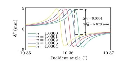
Fig. 6. The intensity sensitivity of refractive index sensor based on OTS-induced PSHE.
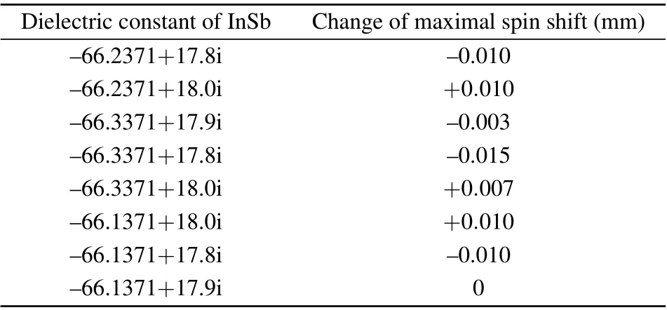
Table 2.The effect of InSb dielectric constant on the maximal spin shift of PSHE.
In practical applications, the experimental growth of InSb/ENZ heterostructure may lead to rough interface of InSb/ENZ. The dielectric constant will be different from the above calculation, therefore, the spin shift and corresponding sensitivity of InSb-DBR-based sensor can be changed. The dielectric constant of InSb at 300 K is –66.2371+17.9i, and the maximal spin shift is 10.9 mm. Here, we calculated the effect of the dielectric constant changes on the maximal spin shift of PSHE, and the detailed data are listed in Table 2. It is clearly seen that the average changing rate of spin shift is about 0.07%, which can be negligible and have little effect on the sensitivity of PSHE-based sensors. Therefore,our proposed gas sensor based on the enhanced PSHE of the InSb-DBR structure shows a good stability in practical experiment applications.
4. Conclusion
In summary, we have proposed the InSb-DBR structure to excite the THz OTS and to achieve the significant enhancement of PSHE for reflected light. The spin shift of PSHE can be dynamically modulated by the thickness of the InSb/ENZ layer as well as the temperature. Under the optimal parameter setup, the largest spin shiftδ+Hwith a 1.1 THz Gaussian beam reaches 11.15 mm,which is much larger than the previously reported values. Finally,a THz gas sensor based on the enhanced PSHE of the InSb-DBR structure due to the excitation of OTS is presented with a superior intensity sensitivity of 5.873×104mm/RIU and good stability. These results could provide an alternative way for enhancement of PSHE in THz range and design of nano-photonic devices.
Acknowledgements
Project supported by the National Natural Science Foundation of China(Grant Nos.12175107 and 12004194)and the Natural Science Foundation of Nanjing University of Posts and Telecommunications(Grant No.NY220030).
- Chinese Physics B的其它文章
- Fault-tolerant finite-time dynamical consensus of double-integrator multi-agent systems with partial agents subject to synchronous self-sensing function failure
- Nano Ag-enhanced photoelectric conversion efficiency in all-inorganic,hole-transporting-layer-free CsPbIBr2 perovskite solar cells
- Low-voltage soft robots based on carbon nanotube/polymer electrothermal composites
- Parkinsonian oscillations and their suppression by closed-loop deep brain stimulation based on fuzzy concept
- Temperature dependence of spin pumping in YIG/NiO(x)/W multilayer
- Interface effect on superlattice quality and optical properties of InAs/GaSb type-II superlattices grown by molecular beam epitaxy

