
Conductance of a single molecule C60-SnPc heterojunction
2022-06-18 03:01YifnWngMingjunZhongJieLiHoTngRihrdBerndtYjieZhngShiminHouYongfengWng
Chinese Chemical Letters 2022年2期
Yifn Wng, Mingjun Zhong, Jie Li, Ho Tng, Rihrd Berndt, Yjie Zhng,*,Shimin Hou,*, Yongfeng Wng,d,e,**
a Key Laboratory for the Physics and Chemistry of Nanodevices and Center for Carbon-based Electronics, Department of Electronics, Peking University,Beijing 100871, China
b CEMES-CNRS, Boîte Postale 94347, Toulouse 31055, France
c Institut für Experimentelle und Angewandte Physik, Christian-Albrechts-Universität zu Kiel, Kiel D-24098, Germany
d Beijing Academy of Quantum Information Sciences, Beijing 100193, China
e Institute of Spin Science and Technology, South China University of Technology, Guangzhou 511442, China
ABSTRACT Geometries of molecule-molecule interfaces strongly influence the current passing from one molecule to another.The contact conductance of molecule-molecule junctions which consist of fullerene and tin phthalocyanine molecules is investigated with a low-temperature scanning tunneling microscope.Two types of molecules are deposited onto Cu(111).Fullerene molecules are transferred to tips through controlled contact of STM tips on molecules.The molecule-molecule junctions are formed by approaching fullereneterminated tips to tin phthalocyanine molecules on Cu(111).Our experimental method can be extended to study the intermolecular charge transport of a range of molecular junctions.
Keywords:Single-molecule electronics Switch C60 Phthalocyanine STM
Molecular electronics can be served as a promising choice to utilize single molecules as building blocks for constructing functional components in electronic circuitry [1–5].Understanding electron transfer at the single-molecule level is indispensable for the construction of electronic devices.A tremendous amount of efforts has been put into investigate the transport of electrons through single molecules.The low-temperature scanning tunneling microscope (STM) is a powerful tool to investigate single molecules on surfaces [6–16].When approaching STM tips to molecules on surfaces, single-molecule junctions with definite geometries can be formed [17].The influence of molecular configuration and orientation on the contact conductance has been well established by this way [18–20].
Not only single molcecules, charge transfer between two fullerene (C60) molecules was thoroughly investigated by cryogenic STM [21].In organic devices, understanding transport properties of organic heterostructures at the single-molecule level plays a more important role in improving their performance.The bulk heterojunction formed byp-type tin phthalocyanine (SnPc) andntype C60molecules has been used to fabricate infrared sensitive molecule organic photovoltaic cells [22].The single molecule C60-SnPc junction can be a model system to study properties of organic hetero-interfaces.In this work, the electron conductance between C60on STM tip and SnPc on Cu(111) is measured.Our results visualize the charge transfer channels in the molecule junction and demonstrate the influence of the contact geometry on the conductivity of molecule junction.
The experiments were performed with a low temperature STM at 9 K with a base pressure of 10-9Pa.The Cu(111) surfaces are prepared by repetitive cycles of Ar ion sputtering and annealing.The etched W tips are indented into Cu(111) in a controlled way to get single-atom tips.C60and SnPc molecules are evaporated from a heated crucible and deposited onto Cu(111) at room temperature.All images were recorded in a constant height mode and processed with the software WSxM [23].
The Sn atom of SnPc does not lie in the molecular plane, as shown in Fig.1a.Therefore, SnPc molecules take two different adsorption geometries on metal surfaces with the central Sn atom either below or above the phthalocyanine plane.They are named by Sn-up or Sn-down molecules and can be easily distinguished by STM images.Fig.1b is the constant current STM image including both Sn-up and Sn-down molecules which exhibit a protrusion or a depression, respectively.

Fig.1.(a) Top view and side view of SnPc.(b) Constant-current STM image of SnPc on Cu (111) obtained with a metallic tip (4.0 × 4.0 nm2; -0.1 V, 0.1 nA).Red and green boxes mark the SnPc-up and SnPc-down molecules, respectively.(c) The schematic diagram of the molecule p-n junction constructed by STM.

Fig.2.(a) Conductance versus tip displacement of a SnPc-up molecule.(b) Conductance versus tip displacement of a Sn-down molecule.Blue stars in both (a) and (b)represent the positions where the contact is formed.
We deposit C60molecules on the Cu(111) substrate partially covered by SnPc molecules.The C60-terminated STM tip is prepared by contacting a metallic tip to a target C60molecule and transferring the C60molecule onto the apex of the tip [24].And then, the C60-tip is used to contact SnPc to form C60-SnPc heterojunction (Fig.1c).During the tip approaching, the tunneling current I is recorded.Typical traces of the conductance (G) as a function of the C60-tip displacement (Δz) are described in Figs.2a and b for Sn-up and Sn-down configuration, respectively.
As the C60-tip approaches towards the center of a SnPc molecule, the conductance rises exponentially in the tunneling region, as shown in Fig.2.The tip displacementsΔzcorresponds to the approaching distance from the position opening the feedback loop.The conductance curve changes smoothly from tunneling to contact, similar to that of C60-C60junction.The contact position is defined as the intersection of the fitted exponential conductance curves in the tunneling and contact regions.The obtained contact conductance of the C60-SnPc junction is 0.0038G0(conductance quantum G0= 2e2/h[25]), which is around two order of magnitude smaller than that of single SnPc or C60.For the SnPc-down molecule, the measured contact conductance using the same C60-tip is 0.0070G0, much larger that of the SnPc-up molecule.Although the contact conductance of C60-SnPc is slightly different for different C60-tips it is always larger for SnPc-up molecules than that of SnPc-down molecules.Sn-down configuration results in a stronger coupling with metal surface states, which enables a more efficient charge transfer at the substrate-molecule interface owing to an extra channel provided by the Sn ion.
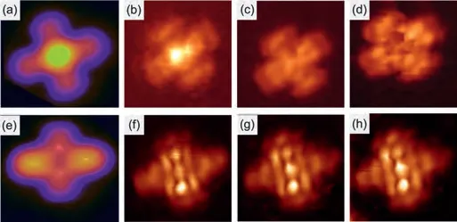
Fig.3.(a) Constant-current STM image of a SnPc-up molecule on Cu(111) obtained with a metallic tip (-0.01 V, 0.1 nA).(b–d) Constant-height STM images of a Sn-up molecule recorded with a C60-tip from tunneling to contact (-0.01 V).(e) Constantcurrent STM image of a SnPc-down molecule on Cu(111) obtained with a metallic tip (-0.01 V, 0.1 nA).(f–h) Constant-high STM images of identical Sn-down molecule recorded with a C60 tip from tunneling to contact (-0.01 V).The size for all images are 4.0 × 4.0 nm2.
For contact curves shown in Fig.2, only the conductance of one C60-SnPc geometry is measured.It is desirable to contact SnPc at different position to compare their transport properties.Therefore,we acquire constant-height STM images of SnPc molecules with the C60modified tip at contact regions to visualize the conductance at various molecular positions.Constant-current STM images of SnPc-up and -down molecules shown in Figs.3a and e are acquiredviametal tip for comparison.Using the C60-tip, constantheight STM images of SnPc-up measured at the tunneling, transition and contact regions are shown in Figs.3b–d, respectively.Notably, the Sn atom of SnPc-up can be considered as probe for “reverse” imaging of the tip-C60molecule.Fig.3b shows a uniformly bright dot that corresponds to a pentagon of the C60cage.Same to the metallic tip, the Sn atom is brighter than lobes in Fig.3b.It means that the geometric structure plays a dominant role for the image contrast.At the transition region, the brightness (conductance) of Sn and lobes looks similar (Fig.3c).At the contact region, the conductance of the C60-SnPc-up junction at lobes of SnPc becomes larger than that at the central Sn region.In contrast,conductance images do not change clearly for the C60-SnPc-down junction from tunneling to contact regions (Figs.3f–h).
It is known that the molecular orbitals close to the Fermi level has a strong influence on the single molecule conductance.To understand conductance maps shown in Fig.3, density functional theory (DFT) calculations are used to calculate orbitals of SnPc and the method has been reported previously [26].The calculated molecular orbitals for SnPc molecules in vacuum are shown in Fig.4 where the upper part shows the orbitals of SnPc-up molecule and the lower part displays those of SnPc-down molecule.The molecular LUMO and LUMO + 1 are degenerated.This means that their energies are at the same level.
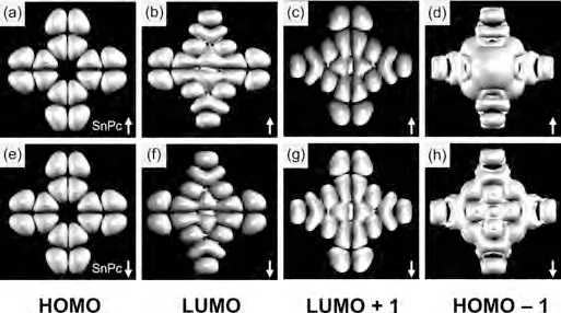
Fig.4.Calculated molecular orbitals of SnPc in vacuum.(a, e) HOMO, (b, f) LUMO,(c, g) LUMO + 1, (d, h) HOMO - 1.The white arrows in the figure represent the Sn down or up with respect the molecular plane.
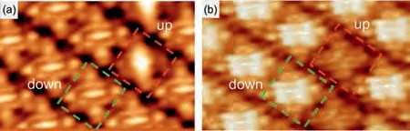
Fig.5.Constant-height STM image of SnPc on Cu(111) obtained via a C60-tip at the(a) tunneling and (b) contact regions.The sample voltage is -0.01 V.Red and green boxes marked the Sn-up and Sn-down molecules, respectively.
For the single-molecule conductance maps, the transport properties of C60-SnPc junctions at various positions are measured.To compare the conductance difference between two SnPc configurations, we perform experiments on the SnPc molecules in the selfassembled monolayer.Fig.5 displays the STM images acquired before and after contact.The molecules in the film adsorb partly with the Sn-up and Sn-down configurations, which are marked by the red and green boxes.At the tunneling region, the image shows a bright protrusion at molecular center for SnPc-up, indicating larger conductivity.At the contact region, the contrast reversal demonstrates that the C60-SnPc-down junction is more conductive compared to the C60-SnPc-up junction, which is consistent with the result of single molecules.
In conclusion, a single molecule C60-SnPc heterojunction has been systematically studies using low-temperature STM and DFT calculation.The influence of contact geometry on the local conductance of the single molecule p-n junction has been well established.Qualitative study of single molecule p-n junction is beneficial for both the construction of single-molecule devices and understanding the relation between structures and performances of the bulk heterojunction layers.
Declaration of competing interest
The authors report no declarations of interest.
Acknowledgments
This work is supported by the Ministry of Science and Technology (Nos.2018YFA0306003, 2017YFA0205003) and National Natural Science Foundation of China (Nos.21972002, 21902003).DFT calculations are carried out on TianHe-1A at National Supercomputer Center in Tianjin and supported by High-performance Computing Platform of Peking University.
 Chinese Chemical Letters2022年2期
- Chinese Chemical Letters的其它文章
- Comment on “Acid-induced tunable white light emission based on triphenylamine derivatives”
- Strategies for efficient photothermal therapy at mild temperatures:Progresses and challenges
- Liposome-based delivery of biological drugs
- Macrophage-targeted nanomedicine for chronic diseases immunotherapy
- Advances, opportunities, and challenge for full-color emissive carbon dots
- Fluorine-containing agrochemicals in the last decade and approaches for fluorine incorporation