Nonvolatile electrical switching of optical and valleytronic properties of interlayer excitons
Tong Ye,Yongzhuo Li,Junze Li,Hongzhi Shen,Junwen Ren,Cun-Zheng Ning,5 and Dehui Li ,2✉
1School of Optical and Electronic Information,Huazhong University of Science and Technology,430074 Wuhan,China
2Wuhan National Laboratory for Optoelectronics,Huazhong University of Science and Technology,430074 Wuhan,China
Abstract Long-lived interlayer excitons(IXs)in van der Waals heterostructures(HSs)stacked by monolayer transition metal dichalcogenides(TMDs)carry valley-polarized information and thus could find promising applications in valleytronic devices.Current manipulation approaches for valley polarization of IXs are mainly limited in electrical field/doping,magnetic field or twist-angle engineering.Here,we demonstrate an electrochemical-doping method,which is efficient,in-situ and nonvolatile.We find the emission characteristics of IXs in WS2/WSe2 HSs exhibit a large excitonic/valley-polarized hysteresis upon cyclic-voltage sweeping,which is ascribed to the chemical-doping of O2/H2O redox couple trapped between WSe2 and substrate.Taking advantage of the large hysteresis,a nonvolatile valley-addressable memory is successfully demonstrated.The valley-polarized information can be non-volatilely switched by electrical gating with retention time exceeding 60 min.These findings open up an avenue for nonvolatile valley-addressable memory and could stimulate more investigations on valleytronic devices.
Introduction
Van der Waals heterostructures(HSs)stacked by transition metal dichalcogenides(TMDs)monolayers enable the generation of long-lived interlayer excitons(IXs)with a large binding energy of about 150 meV1and a long diffusion distance over five micrometers2,further extending the already appealing properties of the constituent TMDs monolayers.Since IXs are composed of electrons and holes that are resided in neighboring layers,their physical properties strongly depend on the layer configurations and external fields or dopings3,4.Through electrical field or doping,we can modulate the emission intensity and wavelength of the IXs5,and even switch its polarization6.Recently,IXs in the HSs stacked by other layered materials such as 2D perovskites and InSe with TMDs monolayer have been demonstrated and can be utilized in mid-infrared photodetections7,8.
In particular,IXs in TMDs-based heterostructures carry valley-polarized information and thus would find promising applications in valleytronics taking advantage of their long lifetime9.Previous studies have demonstrated that IXs exhibit a large valley-polarization degree that can be tuned in a wide range by external electric field10,magnetic field11,and twist-angle engineering12.Although considerable progress has been made in valleytronics,nonvolatile device that is indispensable for valleytronics has not been achieved up to date.Here,we demonstrate an IX-based nonvolatile valley-addressable memory,which would prompt relevant investigations on valleytronics.
Results
In this work,the HS device is formed by a monolayer WS2(top)and a monolayer WSe2(bottom),both of which are contacted with an electrode(Fig.1a).By applying voltage between the electrode and the heavily-doped Si substrate,we can control the doping level of the device when performing optical measurements.Figure 1b shows the optical microscope image of the device.The WS2and WSe2sheets are mechanically exfoliated from their respective bulk crystals and then transferred on a SiO2/p++-Si substrate through dry-transfer technique13.To minimize the generation of bubbles formed between the constituting monolayers,which would suppress the formation of interlayer excitons and thus weaken the switching behavior and chemical-doping effect discussed below,we adopted a tilt-transfer method(see “Materials and methods” section).The edges of the two sheets are also intentionally aligned to improve interlayer coupling3.The device also contains a monolayer WS2/bi-layer WSe2HS region,which is labeled as 1L/2L to distinguish from the monolayer WS2/monolayer WSe2(1L/1L)region.Since the two regions exhibit similar optical behaviors,for a simple discussion,the following text focuses on the measurements acquired in the 1L/1L region of the device,unless stated otherwise.The experimental data collected from the 1L/2L region is provided in supplementary materials(Fig.S1).The substrate was oxygen-plasma cleaned for 10 min before the dry-transfer procedure,so as to make a uniform hydrophilic surface14.
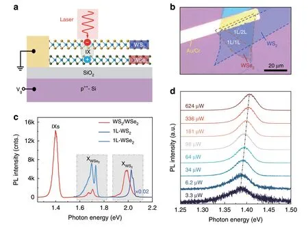
Fig.1 IXs in a WS2/WSe2 HS.a,b Schematic and optical microscope image of the device,respectively.1L/1L and 1L/2L represents monolayer WS2/monolayer WSe2 and monolayer WS2/bi-layer WSe2 respectively.c PL spectra of the HS and monolayer WSe2 and WS2 at 78 K under 23 μW excitation at 532 nm.For a clear visualization,the PL spectrum of individual WS2 is multiplied by a factor 0.02.d PL spectra of the IXs as a function of excitation power under 633 nm laser excitation at 78 K.
IXs in the WS2/WSe2 HS
Figure 1c shows the PL spectra of the HS,from which we can observe severe PL quenching and redshift of the intralayer excitonic peaks,together with the appearance of a low-energy peak at 1.4 eV.The quenching and redshift of the intralayer excitonic peaks can be attributed to interlayer charge transfer15,16and modified dielectric environment17,18,respectively.We assign the peak at 1.4 eV to the IX emission according to previous reports19,20.The excitation-power dependent PL spectra further verify its interlayer nature(Fig.1d).The IX emission peak shows a monotonous blueshift with the increase of excitation power,which is due to many-body effect arising from the repulsive interaction between the dipole-aligned IXs21,22.Such monotonous behavior of IX also manifests that the laser-heating effect can be neglected during the measurements.
Excitonic hysteresis of IXs
To explore gate-dependent features of the IX emission,we measured the PL spectra of the device under cyclicVg,which scans first from 0 to-60 V,then 0 V all the way to 60 V and finally back to 0 V(Fig.2a).The IX emission peak shows a redshift and the emission intensity is enhanced with the decrease ofVg,and vice versa.The redshift of the IX emission peak withVgcan be ascribed to the Stark effect6,which is verified by the opposite shift trend of the IX emission peak in devices with stacking order inversed(Fig.S2).Interestingly,the IX emission peak exhibits a strong hysteresis upon cyclic-voltage sweeping.As indicated by the black arrows in Fig.2a,the peak energy of the IXs at middle 0 V(0V-2)cannot return to the same value of initial 0 V(0V-1),until a further upward scanning that is finally back to 0 V(0V-3).The gate-dependent photon energy and PL intensity can be seen more clearly in Fig.2b,c.For a simple discussion,we only compare the states at 0V-2 and 0V-3.The photon energy of 0V-2 is blueshifted by about 20 meV with respect to that of 0V-3.Meanwhile,the PL intensity of 0V-2 is weaker than 0V-3 with a contrast ratio of about 1.7.It is worth to mention that the light intensity changes non-monotonously asVgdecreases from 0 to -60 V,indicating the occurrence of chemical doping23-25,which will be discussed in the following.The light intensity difference between 0V-1 and 0V-3(Fig.2c)might be due to different levels of chemical doping at the initial and final sweeping stages,because charge density can significantly influence the photoluminescence quantum yield of TMDs-based devices26.
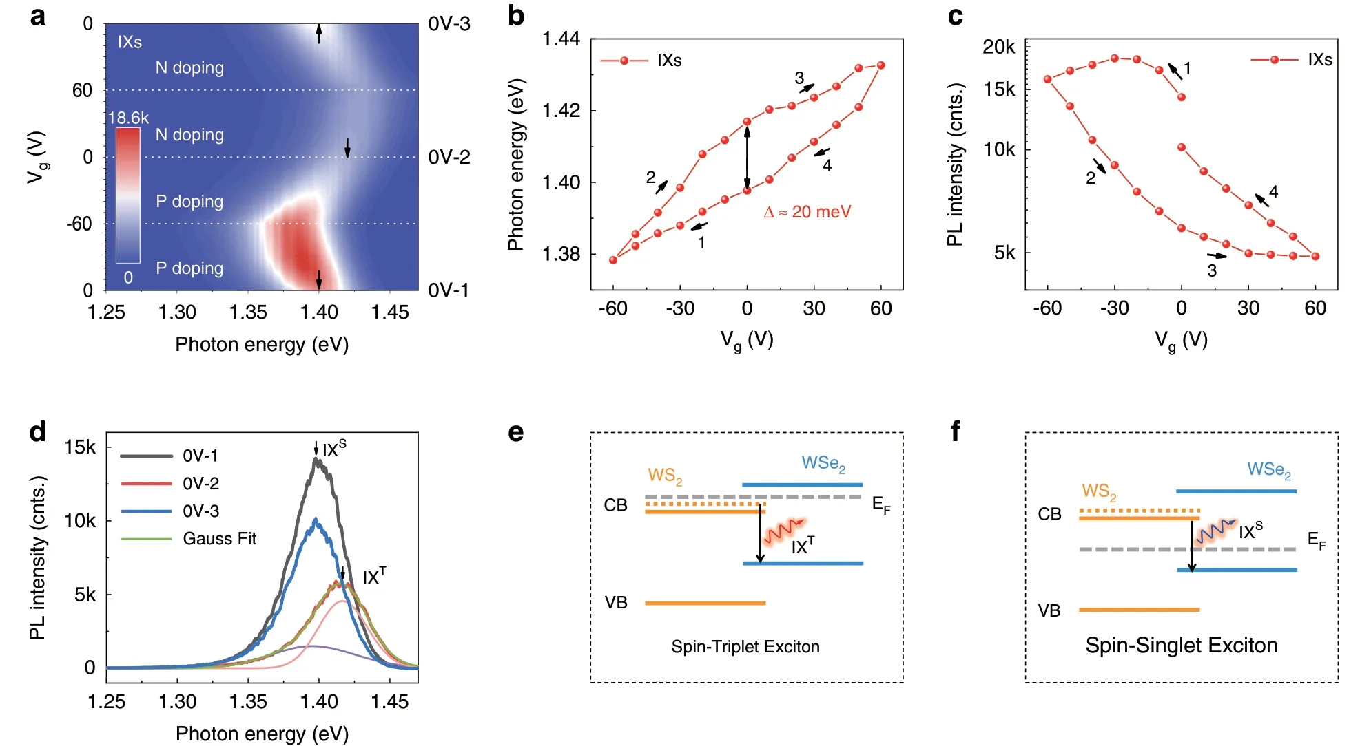
Fig.2 Electrical control of the IX emission.a Contour plot for the PL spectra of IXs upon cyclic Vg.The white dashed lines serve as guides to the eye.Black arrows mark the peak positions of the IXs at 0 V with different scanning sequences.b,c Photon energy and PL intensity of the IX emission as a function of Vg.d PL spectra of the IXs at 0 V with different scanning sequences.0V-1,0V-2,and 0V-3 represent three spectra marked in a.The 0V-2 spectrum is fitted by two Gaussian peaks.The purple and pink lines are attributed to the spin-singlet state(IXS)and spin-triplet state(IXT)of interlayer excitons,respectively.The sample was excited by a 532 nm laser with 23 μW power at 78 K.e,f Schematic of the spin-triplet and spin-singlet excitons.Chemical-doped electrons lift the Fermi level up and shift the IXS to IXT.When those electrons are released,the IXT return to IXS.The orange dashed line stands for the upper spin-splitting conduction band(CB)of WS2.Red and blue arrows represent the recombination paths of the IXs.
As shown in Fig.2d,the IX emission peak of 0V-2 can be decomposed to two Gaussian peaks(detailed fittings of the spectra are provided in Fig.S3).The energy difference of the two peaks is about 20 meV,which is consistent with the splitting energy of the conduction band of WS2(see refs.27,28),strongly suggesting the occurrence of spin-triplet excitons29.This peculiar phenomenon can be understood from the chemicaldoping23,24induced band-filling effect6,as depicted in Fig.2e,f.When the device is chemicallyn-doped,the Fermi level will be lift up and IXs will shift to the spin-triplet state(IXT),which has an inefficient PL yield because of inversed spin.Contrarily,when the chemically-doped electrons are released,IXs will return to the spin-singlet state(IXS).Therefore,the IX emission peaks in 0V-1 and 0V-3 spectra are attributed to IXSemission,and that in 0V-2 spectrum is mainly resulted from IXT.The IXTand IXSpeaks can be well resolved in PL spectra acquired by picosecond laser excitation(Fig.S4a).In addition,the intensity ratio of IXT/IXSincreases with the increase ofVg(Fig.S4b),thus confirming the band-filling mechanism and IXT/IXSorigins.We have also measured the gate-dependent lifetime of the IXs(Fig.S4c-e).The lifetime of the IXs at 0V-2 is slightly shorter than at 0V-1 and 0V-3 rather than getting prolonged,further supporting the IXT/IXSorigins11.
Mechanism of the excitonic hysteresis
Electrical hysteresis has been observed in devices based on two-dimensional materials,such as graphene and TMDs based field-effect transistors30-33.Generally,electrical hysteresis is attributed to the chemical-doping effect by doping species(O2and H2O)that are bound at the device/substrate interface,and/or on the surface of the device34-36.In our case,we propose that the excitonic hysteresis mentioned above is originated from the same scenario.
Since our measurements were performed in high vacuum(≈10-7Torr),the influence of the molecules on the device surface can be safely neglected.Therefore,the excitonic hysteresis is more likely due to the O2/H2O molecules that are trapped at the interface between the HS and substrate.To clarify this,we examine the gatedependent PL spectra of the individual WSe2region(Fig.3a),because WSe2is in the bottom of the HS and directly contacts the SiO2/Si substrate.
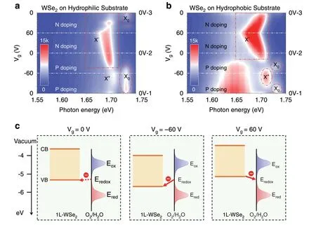
Fig.3 Mechanism of the excitonic hysteresis.a Contour plot for the PL spectra of monolayer WSe2 as a function of cyclic Vg.The spectra were acquired in the individual WSe2 region of the HS on a hydrophilic substrate.b Contour plot for the PL spectra of monolayer WSe2 on a hydrophobic substrate,which is functionalized by hexamethyldisilazane(HDMS).The PL measurements were conducted at 78 K with 532 nm laser excitation(23 μW).c Illustration of chemical doping caused by O2/H2O molecules.The electronic density of states(DOS)reflect the electron energy distribution around the oxidation potential(Eox)and reduction potential(Ered),respectively.Eredox is the energy where the DOS of reducing and oxidizing species are equal: Dox(Eredox)=Dred(Eredox).
The emission features of the intralayer excitons in WSe2are closely correlated to that of IXs.AsVgdecreases from 0 to-60 V(Fig.3a),the emission of positive trions(X+)is gradually enhanced,while the peak of neutral excitons(X0)is suppressed,indicating an efficient hole doping(detailed data is provided in Fig.S5).Peculiarly,asVgincreases from -60 V back to 0 V,the evolution track is asymmetric to that from 0 to -60 V.The trion emission peak is firstly weakened,then enhanced and redshifted with the increase ofVg.The asymmetric evolution strongly indicates the occurrence of negative trions(X-),and suggests that the WSe2is chemicallyn-doped36,37at 0V-2.WhenVgincreases from 0 to 60 V,the X-peak is redshifted further,but with emission intensity weakened because of Coulomb screening from the free electrons38.When voltage scans backward from 60 to 0 V,the Xpeak shows a blueshift and the emission intensity becomes weaker while the X0peak is gradually enhanced,indicating that the chemically-doped electrons have been released.All the above features are well consistent with the previously mentioned chemical-doping effect23,24,36.To further validate such hypothesis,we conducted a control experiment with WSe2monolayer on a hydrophobic substrate(Fig.3b).The evolution tracks of X+andX0emission are roughly symmetrical along the black dashed line at about-60 V.The slight deviation might be due to trace O2/H2O molecules that are adsorbed on WSe2before the transfer procedure.Besides,in sharp contrast to Fig.3a,the track of X-is quasi-symmetrical along the dashed line at 60 V,suggesting that the excitonic hysteresis is largely suppressed.Therefore,H2O molecules should play a critical role in our observations.The unknown peak centered at about 1.65 eV probably arises from dark states,charged dark states and phonon-assisted sideband emission from the dark excitons39,40,which require further investigations.
The surface of SiO2is usually covered with a layer of silanol groups(≡Si-OH),especially after it is treated by piranha solution or plasma cleaner23,36.With these silanol groups,SiO2/Si substrates are easily bound by ambient O2and H2O molecules36.As shown in Fig.3c,the chemical potential of the redox couple(O2/H2O)is about-5.3 eV23,41,which is slightly higher than the valence band of WSe2(about -5.46 eV)42,43.Therefore,electrons spontaneously transfer from O2/H2O to WSe2,making monolayer WSe2initiallyn-doped(detailed information is provided in Fig.S5),and resulting in the asymmetry evolution ofX0in Fig.3a.
When applying negative gate voltages,electrons are forced to transfer further from O2/H2O to WSe2.The chemical-doped electrons are trapped in WSe2whenVgreturns from -60 to 0 V,because the chemical-potential barrier between WSe2and O2/H2O block electrons out(detailed supporting data can be seen in Fig.S6).Consequently,the Fermi level of the HS is lifted up,and IXs shift to the spin-triplet state(Fig.2e)due to the band-filling mechanism4,6.With Fermi level raised up,photon-excited electrons are driven into the upper spin-flipping level due to Coulomb blocking effect.Those chemically-doped electrons balance out the gate modulation,resulting in the non-monotonic behavior of the IXs in 0~-60 V range(Fig.2c)and the excitonic hysteresis.The chemicaldoping effect also explains why X0emission maintains its intensity from 0 to -60 V for WSe2on the hydrophilic substrate(Fig.3a)but greatly suppressed on the hydrophobic substrate(Fig.3b).
When applying positive gate voltages,the chemicaldoped electrons are driven back from WSe2to the O2/H2O redox couple.Therefore,IXs return to the spinsinglet state(Fig.2f)whenVgscans back to 0V-3.This control experiment further verifies the chemical-doping mechanism and well explains the origin of the excitonic hysteresis of IXs shown in Fig.2.The hysteresis is largely suppressed in HSs stacked on hydrophobic substrates(Fig.S7).To demonstrate this,we have also fabricated WS2/WSe2/hBN HSs on hydrophilic substrates with WS2/WSe2HS partially separated from the substrate byhBN with a thickness of around 50 nm.For these devices,the excitonic hysteresis is observed in the region where WS2/WSe2HS directly contacts with the substrate,but absent in thehBN-insulated region(Fig.S8),further supporting the chemical-doping mechanism.Additionally,the area of the hysteresis curve is in proportion to the chemical-doping level,and could be quantitatively controlled by oxygen-plasma-cleaning time of the SiO2/Si substrate as demonstrated in WSe2-based memories14.The hysteretic behavior is re-confirmed by two-cyclescanning measurements(Fig.S9),and well reproducible in multiple repeating measurements and also in different samples.Therefore,we rule out the influence of random contamination.
Valley-polarized hysteresis of the IXs
To study the chemical-doping effect on the valleypolarized features of the IXs,we measured the helicityresolved PL spectra of the device(Fig.4a).Interestingly,the IX peak exhibits a negative circular polarization in contrast to that of intralayer excitons in WSe2and WS2,which can be ascribed to the interlayer quantum interference imposed by the atomic registry between the constituent layers44.To qualify the valley polarization,the degree of circular polarization(DOCP)has been introduced and defined asPc=(I+-I-)/(I+-I-),whereI+(I-)denotes the intensity of co-polarized(cross-polarized)PL component.For the IXs peak,Pc= -12.3%,while for the intralayer excitonic peak of WS2and WSe2,Pc=15%and 7.1%,respectively.It is worth to mention that the helicity-resolved measurement was performed at 78 K with excitation power of about 180 μW.Therefore,the spatial modulation of moiré potential on optical selection rules for interlayer excitons can be neglected,since the moiré trapping effect can only be observed with ultra-low power excitation at ultra-low temperature45.
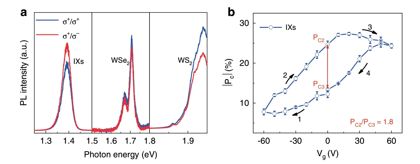
Fig.4 Electrically-tunable valley polarization of the IXs.a Helicity-resolved PL spectra of the HS under 633 nm excitation(180 μW)at 78 K.b Absolute circular polarization degree of the IXs as a function of Vg.The helicity contrast is defined as Pc2/Pc3,where Pc2 and Pc3 is the absolute circular polarization degree at 0V-2 and 0V-3,respectively.The error bars in b represent the uncertainty of the data extraction
The DOCP of the IXs can also be electrically controlled byVg,as shown in Fig.4b(the full data set is provided in Fig.S10).The absolute DOCP is greatly suppressed at-60 V(p-doping),but enhanced at 60 V(n-doping).This phenomenon has been reported byScuriand coworkers,and is attributed to changes in valley-depolarization time caused by electron/hole doping12.Similarly,we believe our observations can be also ascribed to the charge doping from external applied bias and chemical doping(Fig.S4).Interestingly,the DOCP and lifetime(Fig.S4e)of the IXs also exhibit a strong hysteresis,probably due to the carrier trapping and detrapping induced by the above-mentioned chemical-doping,which leads to different doping concentrations and further different valley-depolarization time and DOCP under the same gate voltage.To sum up,the chemical-doping effect leads to the formation of spin-triplet excitons,and gives rise to the hysteresis of excitonic emission,valley-polarization degree and lifetime of IXs,which could find potential applications in nonvolatile valley-dependent information processing.
IX-based valley-addressable memory
To demonstrate the valley-encoding ability of the device,we measured time-dependent PL spectra under circular excitation(σ+),as shown in Fig.5a.As gate voltage cyclically changes among -60,0,60,and 0 V,the photon energy of the IX emission periodically shifts among 1.38,1.42,1.45,and 1.40 eV,which are analogous to the performance of conventional electronic devices under “write”,“read”,and “erase” operations.In addition,the emission intensity also periodically changes in response to those memory operations.Specifically,the intensity level of IXS(IXT)located at 1.40(1.42)eV can be regarded as digital information 1(0),which can persist for a long time with no power consumption,suggesting potential applications in nonvolatile storage.Intriguingly,as the detection helicity switches between σ-and σ+,the PL intensity of the 0 and 1 states exhibit helicity-resolved features.There are four intensity levels emerging,which can be defined as “00”,“01”,“10”,and “11”,indicating valley-encoding abilities of the device.Based on this feature,we can selectively encode/address the valleypolarized information by helicity excitation/detection.

Fig.5 Electrically controlled memory operations in the HS.a Time-dependent IX emission characteristics upon cyclic Vg among-60,0,60,and 0 V.Each voltage lasts for about 4 min.The detecting polarization shifts every three cycles of Vg.b Retention time of the“1”and“0”excitonic states.The writing and erasing voltages last for about 3 min,and the reading voltage lasts for about 64 min.The peak energies and intensities are extracted from real-time spectra,each of which was measured within 10 s.The sample was excited by a 633 nm laser with a power of 180 μW at 78 K.
To evaluate the retention time of the encoded information,we then prolong the reading-operation time,as shown in Fig.5b.Surprisingly,the 1 and 0 excitonic states can persist for at least 60 min,holding great promise for nonvolatile valley-addressable memory.As a matter of fact,the retention time should be much longer than 60 min,as can be seen in a logarithmic-timescale plot(Fig.S11a).This long retention time can be attributed to the synergetic blocking effect of the type-II band alignment of the HS and the chemical-potential barrier between WSe2and O2/H2O(Fig.S6).We also note that the 0(1)state varies dynamically before reaching a steady state.This is probably due to the charging/discharging process of the device,as confirmed by the features oftime-dependent gate current(Fig.S11b).Importantly,the performance of the device is so robust that it can immune laser-heating effect,since the laser was kept focusing on the sample during the measurements.In addition,the information encoding ability of the device can persist up to about 250 K,which is promising for high temperature valleytronic applications(Fig.S12).
Since the nonvolatile valley-addressable memory has never been reported,it is hard to make an objective comparison.Nevertheless,the device is similar to photonic memory,thus we list the parameters of our device and other nonvolatile photonic memories in Table 1,which shows that our device is outperforming in comparison with peer memory devices.The PL ON/OFF ratio of the 1/0 states could be as large as 3.6(Fig.S13),which is larger than peer photonic memories46-49.The power consumption of the device is estimated to be about 74/56 nW for set/reset operation(Fig.S11b),which is extremely low in comparison with other phase-change photonic memories46-49.The switching time of our devices could be very short but limited by our testing system,since the hysteresis effect could be established in several microseconds according to previous reports50.
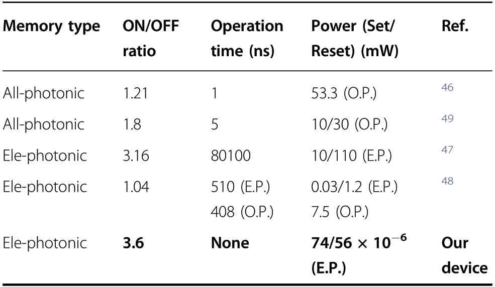
Table 1 Parameters of our device and peer works
Discussion
In summary,we have systematically investigated the excitonic/valley-polarized hysteresis of IXs in a WS2/WSe2HS.By examining the PL spectra of the WSe2monolayers on hydrophilic and hydrophobic substrates,we verify that the origin of the hysteresis is the chemicaldoping of WSe2by O2/H2O redox couple.Benefiting from the hysteresis effect,IXs can be non-volatilely switched between a spin-singlet state and a spin-triplet state,enabling applications in valley-polarized information processing.Finally,we demonstrate the memory function of the device,which shows a good writing/reading/erasing ability with retention time exceeding 60 min.Our study provides a potential paradigm to achieve nonvolatile valley-addressable memory and thus would greatly advance the development of valleytronic devices.
Materials and methods
Sample preparations
Electrodes were fabricated by standard photolithography and thermal evaporation(50 nm/2 nm Au/Cr).The substrates with prefabricated electrodes were ultrasonic cleaned and plasma cleaned for 10 min before the fabrication of the HS.WS2and WSe2monolayer flakes were first mechanically exfoliated onto polymethylmethacrylate(PMMA)stamps,and then transferred on a SiO2(300 nm)/Si wafer using a dry transfer technique with the aid of an optical microscope and a nanomanipulator.The hydrophobic substrates were prepared via immersing in HDMS vapor for 10 min and then rinsing with acetone for 30 s to form a hydrophobic layer on the substrate51.All the samples were not treated by thermal annealing,because this procedure would disable or deteriorate the performance of nonvolatile memory devices.To minimize the generation of interface bubbles,we adopted a tilt-transfer method.The PDMS stamp was tilted for about 2°before transfer,and then pressed down until the upper TMDCs monolayer was approaching the lower one.Afterward,the substrate was heated to 50°C to advance contact frontier forward further,and finally the heater was turned off when the two TMDCs monolayers were well laminated for about 3 min.
Optical measurements
The as-fabricated devices were mounted in a continuous flow cryostat with 10-7Torr vacuum.For gatedependent PL measurement,the sample was excited by a 532 nm laser(23 μW)at 78 K.For the helicity-resolved PL measurement,the sample was excited by a 633 nm laser with a power of 180 μW at 78 K.The time interval between two adjacent spectra is about 1 minute when performing gate-dependent measurements.For the memory operation measurement,the spectra were acquired withVgchanging cyclically and laser keeping focused on the sample.Each spectrum was measured within 10 s.All the PL spectra were collected by a 50×objective lens(N.A.= 0.7)in a Raman spectrometer(Horiba HR550)with a 600 g/mm grating.A Keithley 2400 sourcemeter was used as the voltage source.
Acknowledgements
D.L.acknowledges the support from National Key Research and Development Program of China(2018YFA0704403),NSFC(62074064)and Innovation Fund of WNLO.T.Y.gratefully acknowledges Hao Sun,Danyang Zhang,Jian Zhang,and Jiaqi Wang for the help in conducting experiments.
Author details
1School of Optical and Electronic Information,Huazhong University of Science and Technology,430074 Wuhan,China.2Wuhan National Laboratory for Optoelectronics,Huazhong University of Science and Technology,430074 Wuhan,China.3Department of Electronic Engineering,Tsinghua University,100084 Beijing,China.4Frontier Science Center for Quantum Information,100084 Beijing,China.5School of Electrical,Computer,and Energy Engineering,Arizona State University,Tempe,AZ 85287,USA
Author contributions
D.L.conceived the idea.D.L.and T.Y.designed the original experiment.T.Y.fabricated the devices and performed the photoluminescence measurements.Y.L.and C.-Z.N.help performing the time-resolved PL measurements.J.L.help modifying the pictures.H.S.and J.R.made the hydrophobic substrates.D.L.,C.-Z.N.,and T.Y.co-wrote the manuscript.All authors discussed the results and commented on the manuscript.
Data availability
The data that support the findings of this study are available from the corresponding author upon request.Supplementary information accompanies the manuscript on theLight:Science &Applicationswebsite(http://www.nature.com/lsa/).
Conflict of interest
The authors declare no competing interests.
Supplementary informationThe online version contains supplementary material available at https://doi.org/10.1038/s41377-022-00718-7.
 Light: Science & Applications2022年2期
- Light: Science & Applications的其它文章
- First Chinese ultraviolet-visible hyperspectral satellite instrument implicating global air quality during the COVID-19 pandemic in early 2020
- Toward implantable devices for angle-sensitive,lens-less,multifluorescent,single-photon lifetime imaging in the brain using Fabry-Perot and absorptive color filters
- MXene supported surface plasmons on telecommunications optical fibers
- Phase-matching-induced near-chirp-free solitons in normal-dispersion fiber lasers
- Microsphere-assisted,nanospot,non-destructive metrology for semiconductor devices
- Probing the orbital angular momentum of intense vortex pulses with strong-field ionization
