
Strain of 2D materials via substrate engineering
2022-03-14 09:27YngwuWuLuWngHuiminLiQizhiDongSongLiu
Chinese Chemical Letters 2022年1期
Yngwu Wu,Lu Wng,Huimin Li,Qizhi Dong,Song Liu,∗
aInstitute of Chemical Biology and Nanomedicine(ICBN),State Key Laboratory of Chemo/Biosensing and Chemometrics,College of Chemistry and Chemical Engineering,Hunan University,Changsha 410082,China
bState Key Laboratory of Chemo/Biosensing and Chemometrics,College of Chemistry and Chemical Engineering,Hunan University,Changsha 410082,China
ABSTRACT Two-dimensional(2D)materials have received extensive attention in the fields of electronics,optoelectronics,and magnetic devices attributed to their unique electronic structures and physical properties.The application of strain is a simple and effective strategy to change the lattice structure of 2D materials thus modulating their physical properties,which further facilitate their applications in carrier mobility transistor,magnetic sensor,single-photon emitter etc. In this short review,we focus on the strain applied via substrate engineering.Firstly,the relationship between the strain and physical properties has been summarized.Secondly,the methods for achieving substrate engineering-induced strain have been demonstrated.Finally,the latest applications of strained 2D materials have been introduced.In addition,the future challenges and development prospects of strain-modulated 2D materials have also been proposed.
Keywords:2D materials Strain engineering Substrate engineering Substrate structures Substrate functions
1.Introduction
Since the successful preparation of two-dimensional(2D)graphene in 2004viamechanical exfoliation[1,2],the 2D materials have attracted extensive attention[3-5].Attributed to their unique electronic structure,the 2D materials exhibit excellent morphological[6,7],electrical[8,9],optical[10,11],magnetic[12]and chemical properties[13].Ultra-thin 2D materials refer to the materials with a horizontal dimension larger than 100 nm and the thickness as low as a single or a few atoms(generally less than 5 nm)[14,15].For the ultra-thin 2D material,the electron cloud has been limited in the 2D plane,which is sensitive to external factors[16,17].Recently,researchers have developed various methods to change the electronic structure of 2D materials,thus modulating their properties and accommodating various applications,such as doping[18,19],alloying[20,21],generating defects[22,23],engineering strain[24,25],or van der Waals heterostructures[26].
Among these methods,strain engineering has been one of the simplest and most effective methods to regulate the electronic structure of 2D materials[27].On one hand,the electrons confined in 2D ultra-thin space make the materials sensitive to the strain.On the other hand,2D materials can endure large uniaxial or biaxial strain without the fracture,resulted from their excellent Young’s modulus and deformation properties[28].The properties of 2D materials can be widely controlledviastrain engineering.As the strain regulates the lattice structure of the 2D material,it can adjust various properties,such as phonon mode,band gap,electrical properties,magnetic properties,chemical properties[17,29-32].
Different methods have been applied for strain engineering,which have different features.Microscopic methods such as heteroatom doping[18],lattice defects[22,23]and mismatch[33,34]generate strain by changing the local electronic structure thus regulating the properties of 2D materials.However,such methods are lack of precision and controllability.Macroscopic method control strain through substrate engineering,such as rough substrates[35-38],array substrates[39-42],and flexible substrates[7,43-45].Such methods can accurately adjust the properties of 2D materialsviachanging the electronic cloud and lattice structure,with better controllability compared to the microscopic methods.Flexible[44,45]and rigid substrates[46]have been involved to modulate properties of 2D semiconductors,as well as the atomic force microscope(AFM)probe[47].Therefore,it is necessary to summarize recent advances in substrate engineering-induced application of strain and explore the correlation between strain and properties of 2D materials.
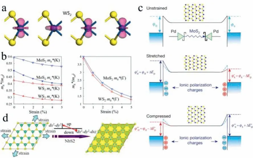
Fig.1.The effects of strain on 2D TMDs.(a)Partial charge densities of WS2.From left to right,the first and second illustration represent conduction band minimum(CBM)and valence band maximum(VBM)states free of strain,respectively,and third and fourth illustration represent CBM and VBM states under 5% strain.(b)The calculated change of effective mass of electron and hole for monolayer WS2 and MoS2.Copied with permission[17].Copyright 2014,John Wiley &Sons.(c)Schematic illustration of piezoelectric effects on modulation of SBH.Copied with permission[29].Copyright 2014,Springer Nature.(d)Schematic illustration of biaxial strain modulated magnetic properties of NbS2.Copied with permission[51].Copyright 2012,American Chemical Society.
In this short review,the latest developments in straincontrolled 2D materials based on substrate engineering have been investigated.Firstly,we demonstrate the effects of strain on 2D materials,from the aspects of lattice structure change,phonon model and band gap.Secondly,we summarize the methods for introducing strainviasubstrate engineering,including substrate preparation and strain introduction.Then,a few examples of the applications of strain engineering to modulate the magnetic,chemical,and optical properties of 2D materials have been introduced.Finally,we put forward some prospects for strained 2D materials.Due to the limited level of knowledge,we could not make a comprehensive summary,and there may be deficiencies.While,we hope that this review can provide insight for the exploration of strain engineering and guide for its applications in 2D materials.
2.Effect of strain on 2D materials
Strain has been widely applied in modulating the optical,electrical,and magnetic properties of 2D materials.The 2D materials with strain-modulated properties have exhibited new applications.Here,the main changes of properties induced by strain in 2D materials have been summarized,including lattice structure,phonon mode and band gap.For exploring the effects of strain quantitatively,the measurement of strain has also been introduced.
2.1.Crystal lattice structure change
Strain engineering of 2D materials can change the lattice structureviaaffecting the electron confined in ultra-thin 2D plane of crystal.For graphene,the carbon atoms arranged in hexagon,and the carbon was sp2hybridized with another p orbital to form theπbond[48].Transition metal dichalcogenides(TMDs),including MoS2,MoSe2,WS2,WSe2,etc.,are another new class of 2D materials with many remarkable properties,with an appropriate band gap[14].For WS2,conduction band and valence band were generated by different parts[17].Conduction band was resulted from the metal d orbital.And the valence band was more complicated,derived from two parts,the dxyand dx2-y2of metal,and pxand pyorbitals of the chalcogen,respectively(Fig.1a).The crystal structure of TMDs may be affected by the mechanical strain,since the strain distorted electron cloud and changed the S-Mo-S bond angle,thus strongly affecting the band structure and enabling the creation of closed patterns for electronics and optics,as well as the effective mass(Fig.1b)[17].Strain functioned in decreasing the band gap and effective carrier mass,thus improving electrical property and carrier mobility.Generally,the band gap would be reduced by about 0.1 eV with 1% strain in biaxial tension[49].
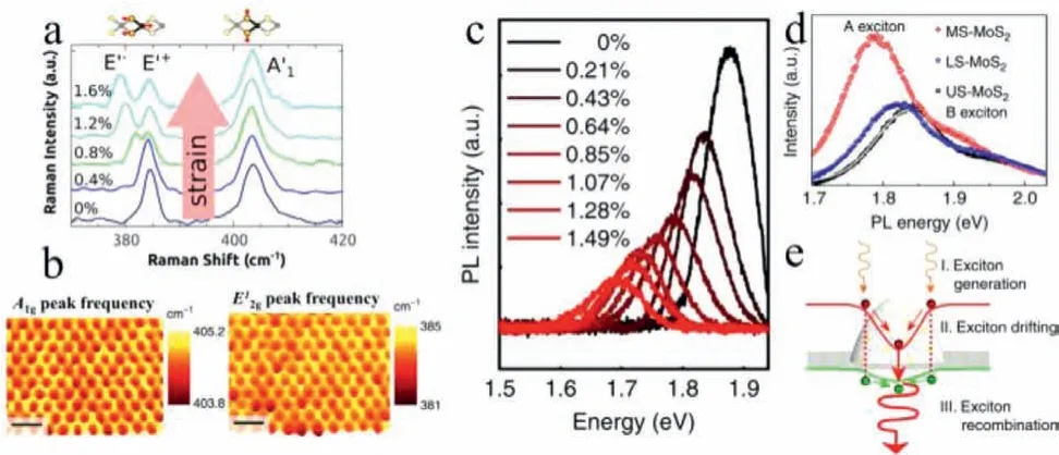
Fig.2.(a)The Raman spectra of monolayer MoS2 under stain from 0 to 1.6%.Copied with permission[53].Copyright 2013,American Chemical Society.(b)The scanning Raman spectroscopic maps with A1g and E12g peaks of MoS2(the scale bar is 1 μm).Copied with permission[46].Copyright 2015,Springer Nature.(c)PL intensity change under different strain from 0 to 1.49%.Copied with permission[55].Copyright 2020,Springer Nature.(d)PL spectra of most strained-MoS2(MS-MoS2),less strained-MoS2(LS-MoS2)and unstrained-MoS2(US-MoS2).(e)Schematic illustration of the funneling effects of excitons due to the localized strain.Copied with permission[46].Copyright 2015,Springer Nature.
Tensile and compressive strain may affect the symmetry of the material,causing changes in the properties sensitive to symmetry.Terraced substrate can generate the topographic corrugation in graphene,which changed the charge density and induce the magnetoresistance[50].Meanwhile,2D materials with noncentrosymmetric structure showed sensitivity to strain-induced local lattice distortion,which can modulate the Schottky barrier height(SBH)and the width of depletion layer[29](Fig.1c).The source area achieved a high piezoelectric potential under compressed strain,attributed to the improved SBH.For the bilayer MoS2,strain can only affect the band gap structure and then change the electric conductivity.Nevertheless,the maximum mobility of MoS2device was up to 850 cm V−1s−1in SiNxcrested substrate,and carrier mobility was improved with the increased surface roughness[36].The improvement in electrical property and mobility may be resulted from two factors.On one hand,the crested substrate can induce strain.On the other hand,the gate-dielectric properties can also make effects.According to investigation on surface of different materials,the electronic properties of devices have been mainly affected by the surface morphology instead of material species.
Strain can also make effects on crystal lattice and electroncloud structure.Thus,it changes the magnetic properties.ReSe2,NbS2and NbSe2under strain exhibited the magnetization properties[31,51].The NbS2and NbSe2under strain show the spinpolarized states(Fig.1d).The magnetic characteristics are the comprehensive result of through-bond and through-space interactions.Hence,strain has been widely studied as an effective way to adjust the crystal structure of materials.It is significant for the preparation and practical application of 2D materials with controllable properties.
2.2.Phonon mode and band gap
The biaxial and uniaxial strain can change the phonon mode due to the soft-mode phonon instability[52].The change of phonon mode can be clearly shown in the splitting and shifting of Raman peak.Bolotin group used curved SU-8/polycarbonate(PC)substrate for applying uniaxial strain to the monolayer and bilayer MoS2devices[53].As shown in Fig.2a,the E’peak(representing the in-plan vibrations)split into two sub-peaks,indicating that the strain breaks the symmetry of crystal rather than A’peak(representing out-of-plane vibrations).Zheng group conducted the Raman mapping on the ‘artificial atom’of MoS2[46].They found that,the frequency of both A’peak and E’peak gradually increased from top to down on the tip of nanocones,where the strain was highest.This phenomenon indicated red-shift in the range of nanocones.As shown in Fig.2b,the shifted Raman peaks under different strain suggest that A’peak was less sensitive than E’peak.Bunch group[54]involved pressure difference to induce biaxial strain(up to 5.6%),obtaining a Raman shift of MoS2at a rate of −1.7 cm−1/% for the A1gand −5.2 cm−1/% for the E12g.
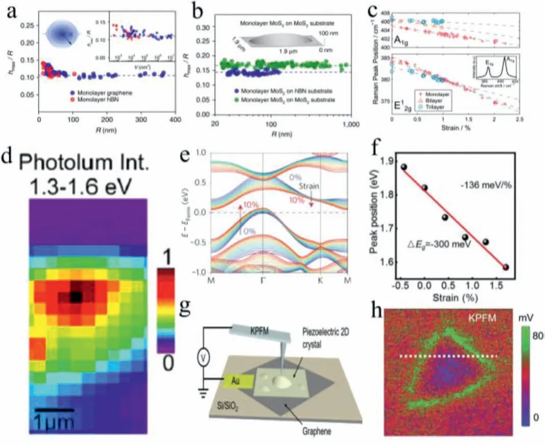
Fig.3.(a)The relationship between aspect ratios and radius of bubbles.(b)Aspect ratio of MoS2 bubbles on h-BN and MoS2 substrates.Copied with permission[58].Copyright 2016,Springer Nature.(c)The relationship between A1g and E12g modes of MoS2 and the strain.Copied with permission[54].Copyright 2016,American Chemical Society.(d)The PL characteristics of MoS2 in the nanopillar structure,and the PL is between 1.3~1.6 eV.Copied with permission[49].Copyright 2018,American Chemical Society.(e)Calculation result of band gap change caused by strain from 0% to 10%.Copied with permission[63].Copyright 2016,Springer Nature.(f)The band gap modulation rate.Copied with permission[55].Copyright 2020,Springer Nature.(g)Schematic diagram of the KPFM measurement process.(h)The KPFM measurements of the surface potential on monolayer h-BN.Copied with permission[66].Copyright 2021,John Wiley &Sons.
The band gap of 2D materials can also be varied with strain.Photoluminescence(PL)spectroscopy is one of the most effective way to discuss the evolution of band gap.Liu group[55]discussed the PL shift of single-layer MoS2(Fig.2c),which was the red shift along with the decreased PL intensity.Its band gap variation can reach up to~300 meV.For the monolayer MoS2,the decrease rate of band gap in K point was lower than theΓpoint,indicating that the band gap was transited from direct to indirect atεof~5%[53].The strain-induced transit between direct and indirect band gaps has also been found in 2D materials family,including WS2,WSe2,BP and so on[56,57].Because strain caused the structure transition of band gap(Fig.2d),it observed the red shift and the intensity decrease of PL,which can be explained by the “funnel effect”[24,46].The photo-generated excitons drifted in the region with the maximum strain,and then concentrated excitons were emitted with longer wavelength(Fig.2e).The phonon mode and band gap have great effects on the properties of electronic and optoelectronic device,such as artificial atoms and single-quantum emitters.
2.3.Measurement of strain
The measurement of strain can better characterize the straininduced changes of properties qualitatively and quantitatively.The strain can be demonstratedviathe changes of morphology and physical properties.The balance of van der Waals forces affected the shape of the bubbles between substrate and 2D crystal,thus varying the strain[58,59].There was a certain relationship between the bubble shape and dimensions.Bubble-induce strain made effects on the raised area,in addition,it would also extend to the distances of>2R from the center.From Figs.3a and b,it is interesting that smooth bubbles exhibit uniform aspect ratio,hmax/Leffis~0.11 for the round bubble(Leff=R),and thehmax/Leff~0.07 for the triangular bubbles(Leff~L).hmax,LeffandRis the maximum height,the base characteristic length and radius of bubbles.The aspect ratioh/Ris defined using the following formula:

whereγis adhesion energies between 2D materials and the substrate,c1is the dimensionless coefficients andYis Young’s modulus of 2D materials.This formula indicates that this ratio is only related to 2D material and substrate,independent with the properties of region trapped in the bubble.Those bubbles can change the lattice then affect the spectral and electrical properties,such as deteriorating interface adhesion[60],changing transport properties[61]andpseudo-magnetism[62].
As mentioned in last section,the phonon mode and band gap of 2D materials are sensitive with the strain.Thus,Raman and PL spectroscopy can be used to determine the change of strain[49](Figs.3c and d).According the theoretical prediction and experiment,the MoS2modes shifted linearly at a rate of −1.7 cm−1/%for the A1gand −5.2 cm−1/% for the E12g[54].The effects of tensile strain on the band gap of MoS2is shown in Fig.3e[63].Through the encapsulation of polyvinyl alcohol(PVA),a higher modulation of the single-layer MoS2can be achieved,with a highest modulation of band gap up to~136 meV/%(Fig.3f)[55].The 2D materials with noncentrosymmetric structure have exhibited piezoelectric properties,thus the strain information of these materials can be describedviavisualizing piezoelectricity.Lanza group applied the conductive AFM toin-situdemonstrate the MoS2piezoelectric currents,which can be as high as 65 mA/cm2under strain with patterned holes[64].However,this method was limited by the conductivity of materials.Woods group observed piezoelectricity of hex-boron nitride(h-BN),then they visualized the change of local electric field around the strained areas using 2D crystal(h-BN or graphene)as substrate[65].Moreover,Cao group[66]developed the kelvin probe force microscope(KPFM)toin-situquantitatively visualize the piezoelectric potential profiles under strain(Figs.3g and h).Several theoretical and experiment methods have been developed in the measurement of strain.
3.Substrate engineering
The substrate engineering refers to the introduction of strainviaflexible or rigid substrates.For the flexible substrate,the strain is applied by stretching or compressing the polymer base.For the rigid substrate,the strain is applied to the surface of the base.Here,the application methods of substrate engineering have been summarized.
3.1.Localized strain
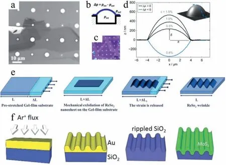
Fig.4.(a)Optical image of graphene flakes with micro-cavity exfoliated on SiO2.Copied with permission[68].Copyright 2018,American Physical Society.(b)Schematic illustration of the MoS2 on the micro-cavity device.(c)The optical image of MoS2 membranes grown via CVD and transferred on the cylindrical cavities(the scale bar is 20 μm).(d)The AFM cross-section with different pressures.Copied with permission[54].Copyright 2016,American Chemical Society.(e)Schematic illustration of the pre-stretched polydimethylsiloxane(PDMS)substrate process for forming ReSe2 wrinkles.Copied with permission[31].Copyright 2015,American Chemical Society.(f)The preparation of the rippled substrate via etching sacrificial layer.Copied with permission[69].Copyright 2017,John Wiley &Sons.
Localized strain enables the local regulation of material properties according to various application methods.When the 2D materials cannot be smoothly matched with another material or substrate,there would be bubble and wrinkle at the interface.Although the number of bubbles can be reduced by annealing,the accumulation of bubbles is still inevitable.The local properties can be varied with bubbles and wrinkles.The generation of bubbles and wrinkles provides a method for studying the strain properties of 2D materials,but the irregular generation of bubbles and wrinkles provides a challenge for quantitative research.For example,the bubbles within heterojunctions would enhance transmission electron microscopy(TEM)selected area electron diffraction pattern contrast.It was amorphous carbon trapped in the stacks,which was unfavorable to transport properties[60,67].However,this method generated bubbles randomly,which was lack of good controllability.Therefore,it is necessary to control the generation of bubbles and wrinkles.Luet al.reported the controllable formation of bubblesviagas diffusion(Fig.4a)[68].Photolithography and etching were applied to achieve hole array,then graphene and MoS2were transferred into micro-cavity and placed in pressure chamber to establish the bubbles.Bunch group produced the bubbles using the pressure difference[54].As shown in Fig.4b,the sample is placed in a high-pressure N2atmosphere,the gas diffuses through the micro-cavity,and then bulged up bubbles between MoS2and micro-cavity.The bubble can be controlled by changing the film and regulating air pressure difference inside and outside.Under the measurement of AFM,the bubbles can be continuously changed between 0.5%-1.5%(Figs.4c and d).
The wrinkling may be varied with the morphology of materials,thus obtaining some functions and properties.Wrinkles show some similarities with bubbles,while there are also some differences,for example,wrinkles induced magnetism[31],anisotropy[69]and optical properties for laser device[70,71].Many methods have been developed to achieve wrinkle on 2D materials,such as mechanical exfoliation,pre-stretched substrate[31],wrinkled substrate[69],micro-tip[72]and transfer processes[61].As shown in Fig.4e,wrinkles can be generated on pre-stretched substrate after mechanical peeling of the ReSe2flakes[31].Molle group reported that rippled pattern assisted the growth of wrinkled MoS2viachemical vapor deposition(CVD)[69].In particular,the substrate patterning was fabricated by sacrificial layer(Fig.4f).The sacrificial layer was made by evaporating the Au film on SiO2,and etched using a gridded porous Ar+source,then the Au film was removed to obtain corrugated SiO2.The rippled MoS2,growing on rippled SiO2,has exhibited many special properties such as anisotropic phonon modes,Raman red-shift and the MoS2work function modulation.All these changes can be regulated with substrate engineering on 2D materials.
3.2.Rough substrate
Compared with bubble and wrinkles,rough substrates have the characteristics of simple preparation and diverse morphology.Rough substrate often has irregular surface,with randomly distributed surface features.The introduction of strain through surface fluctuations has caused the material to control the overall properties of electrical and magnetic properties,which has attracted attention.There are diversified surface characteristics,such as substrate with “hill and valley” structure[73],crested substrate[36],and terraced substrate[50,74].Rrmswas an indicator for describing the surface roughness[75].The measurement of surface roughness and the determination of surface statistics are significant for many applications.Recently,researcher have developed many methods to make substrate roughviasurface treatment and modification,such as etching and spin coating nanoparticles.Rough substrate can change the intrinsic properties of materials,such as promoting the sample synthesis[73,76],boosting the carrier mobility[36],and inducing magneto-resistance[50].The strain on rough surface of 2D materials may make effects on the electronic structures,thus further changing the properties of materials.
The roughness of the substrate can also greatly affect the growth of 2D materials and determined the performance of materials/substrate interface.The large scale preparation of TMDs single crystal has been a necessary way to realize industrial applications[77].The CVD has broad prospects in the growth of single crystal TMDs with large area and in low cost.Some groups have reported the preparation of monolayer TMDsviamolten liquid intermediate process[77]and high melting point sulfur precursor(Na2SO4)[78].However,the substrate also made great effects on material growth during CVD.Zhanget al.prepared a large area of MoS2single crystal on unpolished rough substrate,on which the“hill and valley” structures exhibited theRrmsof 244 nm(Figs.5a and b)[73].The nucleation density can be effectively restrained with the structure on rough SiO2/Si.Furthermore,the suspended growth rate obtained on rough surface was three times larger than that of supported growth rate on polished surface.Moreover,rough substrate influenced the growth of grain boundaries on specified locations and misfit angles(Fig.5c)[35,79,80].The “hill and valley” structure may induce strain and expand,thus changing the PL spectra.The strain and charge doping on MoS2depend on different physical and chemical characteristics of the substrate surface.When the substrate became smoother and chemically inert,the strain and the charge doping would be decreased.With the aid of the standard deviation of the AFM depth profile fitted by the Gaussian curve,the surface roughness can be quantified[38].The surface of amorphous SiO2was determined to be the roughest,followed by sapphire mica and h-BN.
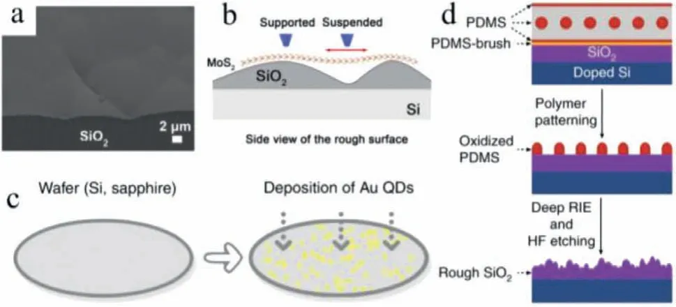
Fig.5.(a)The tilted scanning electron microscope(SEM)image of substrate.(b)Schematic illustration the MoS2 growth process in rough substrate.Copied with permission[73].Copyright 2019,Elsevier.(c)Represent spin coating Au quantum dots to from rough substrate.Copied with permission[35].Copyright 2020,Springer Nature.(d)Schematic illustrated of the process to preparation crested substrate.Copied with permission[36].Copyright 2019,Springer Nature.
Similar researches have been performed on the MoS2.The crested substrate can be achieved by surface etching.Recently,Garajet al.have reported a method to greatly enhance the carrier mobility of MoS2,with an average value of 450 cm2V−1s−1on the crested substrate[36].The two-step photolithography and mask etching were used to adjust the surface morphology and obtain a rough SiO2substrate with aRrmsof 0.5 nm(Fig.5d).In another method,the c-SiNx substrate was processed with hot orthophosphoric acid(H3PO4),thus achieving a terraced substrate with remained dielectric properties and aRrmsof 2 nm.According to statistical analysis of different materials with varied surface roughness,the electronic properties of devices were mainly affected by the surface morphology instead of the material specie.Roughness has provided a new insight for the growth and property regulation of MoS2and other 2D materials,which can be realized with many methods,such as surface reconstruction and selective etching.
Sapphire substrate has been a substrate compatible with surface reconstruction and selective etching.The surface morphology of the sapphire substrate can be reshaped at high temperature(950 °C)and reconstructed to be a step pattern parallel to the[110]direction[76].Step pattern facilitated the directional growth of 2D materials and provided a method for preparing stepped structure.The SrTiO3(STO)substrate[50]can be soaked in demineralized water to form Sr-hydroxide,and then selectively dissolved with HF.The chemical reaction was:SrTiO3+ H2O=Sr(OH)2+ TiO2,Sr(OH)2+ 2HF=SrF2+ 2H2O.The atomically flat terraces and steps can be obtained with the termination of TiO2,and such a substrate can induce magneto-resistance in graphene.Therefore,rough substrates have expanded the methods for the growth of MoS2and other 2D materials on fabricated device.In addition,the properties of 2D materials can be further exploded,such as carrier mobility and magnetism.
However,the rough base is usually irregular,and the surface has a random structure.Therefore,the controllable adjustment of the performance of the 2D material with the rough base is a problem that needs to be solved.
3.3.Array substrate
The array substrate is a way that the substrate regularly introduces strain.Compared with the rough substrate,the array substrate can controllably introduce the strain source through the controllable change of the array unit size(height,width,etc.),which provides a basis for establishing the relationship between the size of the substrate and the magnitude of the strain.It helps to promote the application of strain in a large-area array of 2D materials.Thus,it is beneficial to explore the changes of properties of 2D materials prepared on array substrate.Array with different morphology and thicknesses enriches the regulation form,which is conductive to exploring the relationship between array patterns and material properties.There are several effective strategies to make arrays,such as tera-fab printing[81],thermal-growth[82],etchingbased array[46],evaporating-based array[83].

Fig.6.(a)Schematic illustration of tera-print technology for fabricating halide perovskite nanocrystal arrays.(b)Fluorescence micrograph of halide perovskite nanocrystal arrays.Copied with permission[81].Copyright 2020,American Association for the Advancement of Science.(c)The SEM images of the as-grown InGaN(left)and a smooth top c-plane surface(right).Copied with permission[82].Copyright 2019,American Chemical Society.(d)Schematic illustration of the monolayer-MoS2/ZnO heterostructure arrays.Copied with permission[84].Copyright 2019,American Chemical Society.(e)Tilted false-color SEM image of MoS2.Copied with permission[46].Copyright 2015,Springer Nature.(f)SEM image of MoS2 suspended on SiO2 pillar array.Copied with permission[49].Copyright 2018,American Chemical Society.
The tera-print technology has been applied to fabricate halide perovskite nanocrystal arrays and methyl-ammonium lead bromide(MAPbBr3)nanocrystals on silicon substrate[81].As shown in Fig.6a,the ink was spin-coated on the PDMS micro-pyramidal pens(~1000)array,and then printed on the surface of the silicon wafer.After the evaporation of solvent,the perovskite nucleated and grew.In particularly,the MAPbBr3nanocrystals of~50 nm can be formed with PDMS pens of about 1 μm.A uniform MAPbBr3nanocrystal dot array can be formed on Si wafer(Fig.6b).Moreover,direct growth array is also a widely studied method to prepare array substrate(Fig.6c).Samuelson group used seed induction to grow high in-content InGaN nano-pyramid array[82].The GaN and SiN were deposited on the Si wafer successively,and the SiN was etched to form an arrayviareactive ion.Then the GaN seed was grown by metal-organic vapor phase epitaxy(MOVPE)to induce the formation of InGaN nano-pyramid array.In addition,the InGaN can be etched from pyramids to platelets under the annealing with NH3.One-dimensional nanopillar arrays have also been applied to prepare array substrates(Fig.6d),based on strain engineering to induce strained 2D materials.Thermal growth has been applied for constructing ZnO semiconductor nanorod arrays(NRAs)[84].Then,MoS2was transferred by poly(methylmethacrylate)(PMMA),and a biaxial strain can be induced from 0 to 0.6%.Through the Raman mapping position of the E12g,the periodic distribution of tensile strain of monolayer MoS2on the ZnO nanorod array was determined.At the same time,it found that the strain-induced PL intensity of MoS2was decreased by more than 50%.Above methods provide the strategy to achieve the controllable fabrication of various array substrates,which is the basis for their applications in strain engineering.
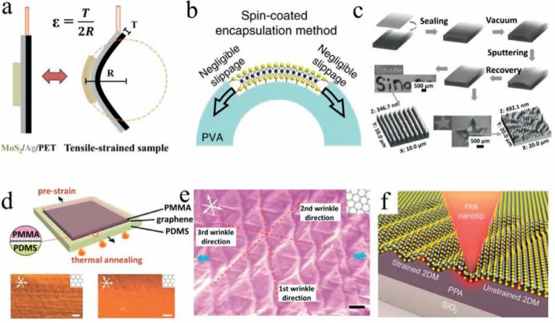
Etching has been another most widely used methods for preparing arrays,which usually requires templates such as nanoparticles,metal mask and photoresist mask.For example,nanoparticles were spin-coated as mask and the nanocone array can be thus obtained with further etching[85,86].Polystyrene or SiO2nanospheres were also spin-coated on the silicon wafer and etched with oxygen plasma to form a mask.Then,the substrate was etched with fluoroform(CHF3)and oxygen plasma.A SiO2nanocones array can be finally obtained after removing nanospheres.MoS2was then transferred by using ethylene glycol,thus producing capillary force during evaporating.MoS2sheet would be pulled down,thus covering the surface of nanocones(Fig.6e).The local biaxial tensile strain at the tip of the nanocone was as high as 2.85%,which was measured by scanning tunnelling spectroscopy(STS).Ouerghi group[49]obtained the pillar array through the metal mask etching method.And then,MoS2was transferred and suspended on Si/SiO2pillar arrays,resulted in biaxial strain on the MoS2(Fig.6f).In particularly,the correlation between nanoscale contribution and design of pillar array has been established with Raman and PL spectroscopy.MoS2mechanical resonator was assemble,presenting a homogeneous along resonator frequency under specific geometry.When the MoS2formed a tent structure(2R< Flexible substrate can be bent and stretched under external mechanical force,thus strain can be applied and transferred to the single layer or a few layers of 2D materials on the substrate.The advantage of applying strain on the flexible substrate is that flexible substrate can be used to control the 2D material in a larger strain range,and to explore the properties and applications of the 2D material.The common flexible substrates are usually organic polymer,such as PDMS,polyethylene terephthalate(PET),PC,PVA.The MoS2film was stripped by chemical exfoliation and printed on the working electrode(Ag/PET substrate)[87](Fig.7a).By stretching the PET substrate,the maximum strain of MoS2on the substrate reached 0.02%.When the tensile strain applied on substrate varied from 0%~0.02%,the hydrogen evolution reaction(HER)current density raises from 31 mA/cm2to 48 mA/cm2at −0.6 V.When the tensile strain was 0.02%,the Tafel slope of MoS2was 135 mV/dec,lower than that of without strain(145 mV/dec). However,placing the material directly on the flexible substrate can easily lead to strain failure due to interlayer slipping or cracking.Researchers have reported some better ways to avoid slipping between layers.Bolotin group included curved SU-8/PC substrate for applying uniaxial strain to the monolayer and bilayer MoS2devices[53].At the same time,they observed that there was a significant red-shift in PL peak signal of monolayer MoS2.It indicated that the in-plane tensile strain can adjust the optical band of MoS2,and there was almost a linear change between red-shift of A peak and the strain,with a change rate of 45 ± 7 meV/% strain.Atεof~5%,the single layer MoS2was transformed into an indirect band gap material,corresponding to a strain of 1.3 ± 0.6%.Similarly,in order to avoid slippage between the material and the substrate,Liu group[55]used PVA encapsulation to achieve a higher modulation for the single layer MoS2(Fig.7b).Its band gap modulation can reach up to~300 meV,with the highest modulation of~136 meV/%. The wrinkle may accommodate the structure of materials to change some functions and properties.For example,previous study showed that the optical band gap of graphene was opened by bending along the nano-trenches.Maet al.reported a novel strategy to control wrinklingviachanging pressure[88].As shown in Fig.7c,the wrinkling can be induced from air bubbles by PDMS device.During Au sputtering under negative pressure,thin Au-PDMS covers were stretched.The effects from strain on graphene mainly had two aspects:positive and negative.For one thing,the interface effects of graphene can be improved thus enhancing the chemical reactivity.For another,the electron–hole puddles can be formed thus decreasing the carrier mobility and suppressing the weak localization.However,it is difficult to achieve an ordered surface wrinkle than that of disordered.Thiet al.reported that 2D ordered surface wrinkle patterns can be spontaneously generatedviathermal strain and vertical spatial confinement on isotropic surfaces,which achieved a high periodicity and crystal symmetry[89].Isotropic materials on the atomic scale,such as graphene and MoS2,have isotropic in-plane mechanical properties.For the crystal structure of graphene,monolayer graphene along zigzag directions had low formation energy,indicating that regular pattern may be obtained under equal biaxial strain following this direction.Sequential wrinkling can be realized on 2D materials through spatial confinement in different directions.The monolayer graphene was transferred onto uniaxially pre-stretched(30%)PDMS substrateviaPMMA.Then the wrinkles were produced through annealing,while graphene/PDMS or graphene/PMMA layer was easy to slide.After annealing,the PMMA was removedviaacetone.There were three main types of angle in the wrinkles,with the angle difference of 60o.It was consistent with the zigzag direction of graphene(Figs.7d and e). The 2D TMDs material has an atomic-level thickness,with van der Waals force between the material and the substrate.The strain on the material can be achieved by bending and stretching the flexible substrate,or conducting thermal conduction.For example,the band gap of the 2D materials can be precisely modulated through thermal scanning probe lithography(Fig.7f)[90].Changes can be induced in the crystal lattice of materials,thereby regulating the properties of TMDs materials.The strain induced by using a flexible base has the advantages of simplicity,directness,facility,and strong scalability.So,it has become one of the most widely used methods. Since the properties of 2D TMDs can be regulated with strainviasubstrate engineering.Various substrates have been applied,such as substrate with local strain,substrate with patterns,substrates with different functions,and flexible or stretchable substrates.Such 2D TMDs with strain-modulated characteristics have been included in various devices,such as field effect transistors(FET),magnetic detectors device,and electrochemical hydrogen evolution. Fig.7.(a)Schematic illustration of the sample with tensile strain,where ε is tensile-strain ratio, R is bending radius and T is the thickness of PET substrate.Copied with permission[87].Copyright 2014,American Chemical Society.(b)Schematic illustration of device structure of MoS2 with tension strain.Copied with permission[55].Copyright 2020,Springer Nature.(c)Schematic illustration of wrinkle formation by bubble.Copied with permission[88].Copyright 2010,the Royal Society of Chemistry.(d)Schematic illustration of graphene sample placed between the PMMA and pre-strained PDMS.(e)SEM image of graphene wrinkle following the crystal orientation.Copied with permission[89].Copyright 2020,American Chemical Society.(f)Schematic illustration of nanopatterning with thermomechanical nanoindentation.Copied with permission[90].Copyright 2020,American Chemical Society. Fig.8.(a)AFM image of terrace substrate.(b)Surface height profiles along the line of(a).(c)Schematic illustration of a top-gated terraced single-layer device.(d)The relationship between Rxx and MR of a magnetic field near the charge neutrality point(CNP).Copied with permission[50].Copyright 2020,John Wiley &Sons.(e,f)Fe3GeTe2 atomic lattice structure and device structure(the scare bar in Fig.8e is 10 μm).(g,h)Magnetization reversal with tension strain changed from 0.65% to 0.71% at 0.2 T and−0.19 T,respectively.Copied with permission[92].Copyright 2020,John Wiley &Sons. Since strain can change the crystal structure and vary the band gap,thus inducing spontaneous polarization and disorder to cause variations in the magnetic properties of the material.On one hand,the strain can modulate the magnetism in 2D magnetic materials.One the other hand,the strain can induce the magnetism in nonmagnetic materials. Terraced substrate has been a special rough substrate which can be achieved by annealing and etching.High-temperature annealing may reconstruct the C-plane of sapphire and form terraced structure[76].It was beneficial to the CVD growth of highly oriented,continuous and uniform monolayer MoS2films[91].The growth was guided by step atoms on the sapphire surface,leading to step-edge-guided nucleation and growth along the edge of the step.Terraces and step can be also achieved through chemical etching.Ariando and co-workers[50]reported the colossal magnetoresistance of monolayer graphene can be obtained at room temperatureviaselective dissolution of special STO(Figs.8a and b).It can be up to 5000% at 9 T on a TiO2-terminated SrTiO3terraced substrate(Figs.8c and d).Rather than surface termination,the giant magnetoresistance was attributed to the graphene disorder,resulted from topographic corrugations and inhomogeneous charge puddles of substrate.The scattering may be remarkably increased under magnetic field.Moreover,the Dirac cones can be also preserved on the STO substrate,which may provide a chance to induce pseudomagnetic field(PMF)in strain.This result provides a new perspective to tailor the magnetism of 2D materialsviaterraced substrate-based strain engineering,which may facilitate their potential applications in magnetic sensors. Wrinkle structure may also induce magnetism in ReSe2[31].The ReSe2lattice is a low symmetry structure,in which the Re atoms forms a Re4“diamond unit” structure to form a “diamond chain”.By mechanical exfoliation,ReSe2film was deposited on the pre-stretched and elastomeric substrates(Gel-PAK film WF-40-X4).After releasing the stretched substrate,the ReSe2with wrinkles perpendicular to the axial direction of the substrates can be generated.When ReSe2with the thickness of 1 nm produced folds with the height of 100 nm and width of 1 μm,the local strainεwas about 1.64%.Under the measurement in the magnetic force microscopy(MFM),there was MFM phase and amplitude image affirm,which was inducing a local spin polarization and making the ReSe2magnetic at the strained region. Fig.9.(a)Schematic illustration of the HER process of MoS2 on Au surface under strain.(b)The scanning transmission electron microscope image of monolayer MoS2 on NPG substrate and the change of Mo-S-Mo bonding angles.Copied with permission[93].Copyright 2014,John Wiley &Sons.(c) ΔGH versus strain intensity with different concentrations of S-vacancy.(d)The polarization curves of the as-transferred MoS2(strain:0% and S-vacancy:0%),strained MoS2 without Svacancies(S-MoS2,strain:1.35% ± 0.15% and S-vacancy:0%),unstrained MoS2 with S-vacancies(V-MoS2,strain:0% and S-vacancy:12.5% ± 2.5%),and strained MoS2 with S-vacancies(SV-MoS2,strain:1.35% ± 0.15% and S-vacancy:12.5% ± 2.5%).Copied with permission[63].Copyright 2016,Springer Nature. The strain applied by the flexible substrate can modulate the properties of the magnetic material like Fe3GeTe2(FGT).Miao group exerted uniaxial tensile strain on Fe3GeTe2by stretching the polyimide(PI)membrane(Figs.8e and f)[92].The strain of 0-0.63% was applied at 1.5 K,and the coercive force field(Hc)was increased by 150% under the strain of 0.32%.WhenTwas lowered to 160 K from 180 K,the hysteresis loop indicated labyrinthdomain ferromagnetic states.WhenTwas 130 K,the hysteresis loop changed under the strain adjustment and became a regular rectangle.There was a transition between single- and labyrinthdomain states,due to the strain-regulated change of transition temperature.The significant enhancement ofHcunder strain in FGT provided a method for strain-assisted magnetization reversal.The magnetic field was swept from −0.4 T to 0.2 T when the strain was 0.71%,and the magnetization direction was up.When the strain was reduced from 0.71% to 0.65%,the signal ofRxywas changed from negative to positive,indicating that the magnetization was reversed under magnetic field of 0.2 T.The transformation of supersensitive magnetism was realized by strain,which was reversible.TheHccan be effectively manipulated.Under tensile strain,the strain change required for magnetization reversal in FGT is about 0.06%(Figs.8g and h),which is much smaller than that of required for spin tilt in the traditional ferromagnetic layer used for magnetic tunnel junctions. Strain has been widely applied in varying the physical properties rather than chemical properties of materials.In this section,the effects from strain on the electrochemical hydrogen evolution of the flexible and rigid substrates have been introduced. A three-dimensional(3D)nanoporous metal supported MoS2film has been constructed for HER[93].The monolayer MoS2film was directly grown on the 3D nanoporous gold(NPG)curved internal surface,which was uniform with severe distortion(Fig.9a).The curved gold surface changed the S-Mo-S bonding angle and then distorted the MoS2lattice(Fig.9b).The changed S-Mo-S bonding angle can improve the charge density of S atoms and lead more negative adsorption free energy(ΔGH).The monolayer MoS2directly contact the highly conductive gold,thus inducing the interlayer potential barrier(forming Ohmic contact)and increasing the charge transfer rate and HER efficiency.Monolayer MoS2@NPG showed high catalytic activity under strain,with a Tafel slope of 46 mV/decade and an onset potential of 118 mV.However,the hydrogen absorption performance should be still improved. Rigid substrate can play the same role with flexible substrate in the application of strain.Sulphur vacancies can be integrated with strain to activate 2H MoS2for hydrogen evolution[63].Tensile strain was applied by using surface tension(1.35% ± 0.15%).The sulfur vacancies were introduced with plasma,resulted in new bands in energy levels.When tensile strain was applied,the new band moved to the Fermi surface to reduce the band gap and increased the number of gap states near the Fermi level,which also enhanced the adsorption strength at the S-vacancy site.Moreover,stretching the sulfur vacancy energy can also changeΔGH.As shown in the Fig.9c,ΔGHapproach to zero can be obtained with the appropriate concentration of sulfur vacancies and strain level,enabling the improvement of the hydrogen absorption activity of MoS2.After comparing the polarization curve of several materials,including Au,MoS2(pristine),S-MoS2(strain),V-MoS2(vacancy),SV-MoS2(strained vacancy)and Pt,it indicated that strain had only limited effects on the enhancement of HER properties of MoS2,which can achieve a current density 10 mA/cm2at -0.17 V and Tafel slop lower to 60 mV/dec(Fig.9d).Moreover,it provided a deep understanding into the correlation of free energy and the combined effects of vacancy with strain.In addition,the Zeng group used density functional theory(DFT)calculations to reveal the relationship between the HER performance of 2D materials(GeP3and SnP3)and the strain[94].The HER performance of GeP3and SnP3was seemed to be insensitive to strain.However,when the materials were attached to graphene,the external strain can vary theΔGHof the GeP3@graphene and SnP3@graphene,which was proportional to the total energy difference.This provided a new idea to understand the relationship between strain,support materials and hydrogen absorption. Strain is an extremely effective way to adjust the 3D carrier confinements to form a PL center[95,96],which has potential applications to achieve quantum emission.Atature group placed the TMDs on patterned arrays of nanopillars with the heights ranged from 60 nm to 190 nm,which were fabricated with electron beam lithography(Figs.10a and b)[39].The strain applied on TMDs led to quantum confinement of excitons,which generated quantum light emitters in the semiconductive layered materials,specially WSe2and WS2[97-102].Single quantum light emitters tended to be generated in arrays with higher nanopillars.Helium ion exposure can also introduce the electron-hole complexes at defect states as optically active states[23].Quantum confinement state can tailor quantum emitters(Figs.10c and d).Recently,the researchers have focused on Au arrays.Strauf and coworks reported Au nanocube cavity array as strain source to induce single-quantum emitters in monolayer WSe2.The monolayer WSe2was stamped onto the array(Fig.10e)[103].Hot sports are located at the four corners,coincident with the strain regions(Fig.10f),which inducing quantum emitters are high as 95% at per site(Figs.10g and h).Zahn reported a giant enhancement of the gapmode tip-enhanced Raman scattering(TERS)signal from a monolayer MoS2flake stamped on Au nanocluster arrays[104].They observed a TERS enhancement of 5.6 × 10⁸and a spatial resolution of 2.3 nm.The strain induced strong carrier localization and changed the dielectric environment single-particles states,which was increased with the aspect ratio(h/r:radiusrand heighth)[96].Strain,as an effective method to promote the localization of strong carriers,is the main source of single photon emission. Fig.10.(a)The process of device fabrication.(b)PL spectra for nanopillars.(c)The second-order photon correlation function g(2)(τ),which represents single-photon emission properties based on(b).(d)Dark field optical microscopy image of monolayer WSe2 on the nanopillar substrate with the height of 130 nm and separation of 4 μm.Copied with permission[39].Copyright 2017,Springer Nature.(e)Schematic illustration of monolayer WSe2 coupled with Au array.(f)Top:the distribution profile illustrating the confinement of the plasmon.Bottom:the highest strain area at cube corners.(g)Hyperspectral PL map of WSe2,strained by Au array within the range of 750-850 nm.(h)The single-photon emission properties.Copied with permission[103].Copyright 2018,Springer Nature. 2D materials have been extensively studied for their excellent physical and chemical properties.However,the properties of 2D materials are closely related to the substrate and external strain.Therefore,both the type and morphology of the substrates may affect the strain thus regulating the physical and chemical properties of the 2D materials. This article has summarized recent advances in the application of strained substrate to regulate the properties of materials.The lattice structure of substrate can be varied,and the symmetry can be changed to regulate the optical,electrical,magnetic,electrochemical properties.Various substrates have been involved,such as the rough substrates,array substrates,and flexible and stretchable substrates.The methods for generating strain and controlling the properties of materials have been introduced,in the fields of optoelectronic devices,magnetic detectors,electrochemical hydrogen absorption and so on.However,besides of strain and substrate,multiple other factors may also affect the properties of material.Therefore,there are still challenges in the accurate understanding and design of substrates morphology for controlling material properties.However,due to the diversity of substrate materials,it is also a problem that needs to be solved to understand the influence of substrate materials and substrate strain on the properties of 2D materials.Therefore,it is necessary to accurately understand the relationship between structure and performance. In general,the strain engineering of substrates provides an effective method for regulating the properties of materials,and also expands their future applications.Multiple innovative materials are emerging with promising prospects,including high-performance MoS2FET with crested substrate,graphene magnetic detector with terrace substrate,quantum light source with patterned substrate and high-performance electrochemical activity.As well as photodetectors[6,105]and wearable devices[106-108]based on flexible substrate.These devices provide useful information for the large-scale development and application of 2D materials in microelectromechanical systems. The authors declare that they have no known competing financial interests or personal relationships that could have appeared to influence the work reported in this paper The work gratefully acknowledges financial support from the National Natural Science Foundation of China(No.21975067)and Fundamental Research Funds for the Central Universities from Hunan University.3.4.Flexible substrate
4.Applications

4.1.Magnetic sensors
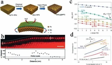
4.2.Hydrogen evolution reaction
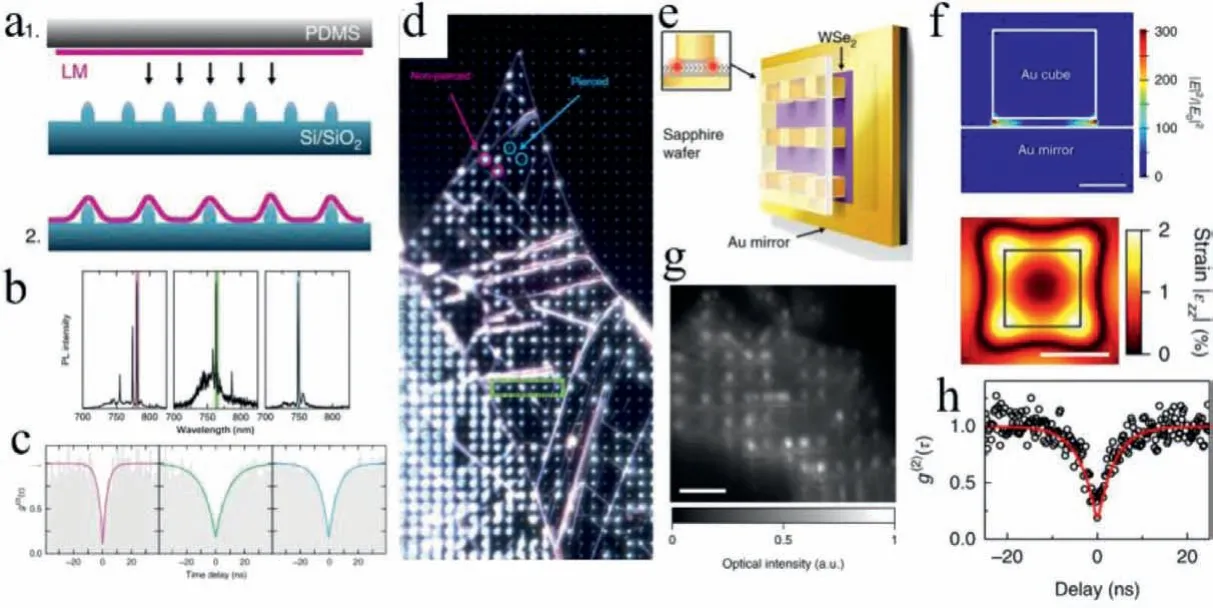
4.3.Single-photon emitters
5.Summary
Declaration of competing interest
Acknowledgments
 Chinese Chemical Letters2022年1期
- Chinese Chemical Letters的其它文章
- Engineering carbon nanocatalysts towards efficient degradation of emerging organic contaminants via persulfate activation:A review
- Recent advances in nanoscale metal-organic frameworks biosensors for detection of biomarkers
- Porphyrin-based heterogeneous photocatalysts for solar energy conversion
- Systematic evaluation of advance in application and discharge mechanism of solution electrode glow discharge
- Insoluble carbonaceous materials as electron shuttles enhance the anaerobic/anoxic bioremediation of redox pollutants:Recent advances
- Selective N-terminal modification of peptides and proteins:Recent progresses and applications