A high-quality-factor ultra-narrowband perfect metamaterial absorber based on monolayer molybdenum disulfide
Liying Jiang(蒋黎英) Yingting Yi(易颖婷) Yijun Tang(唐轶峻) Zhiyou Li(李治友)Zao Yi(易早) Li Liu(刘莉) Xifang Chen(陈喜芳) Ronghua Jian(简荣华)Pinghui Wu(吴平辉) and Peiguang Yan(闫培光)
1Joint Laboratory for Extreme Conditions Matter Properties,Southwest University of Science and Technology,Mianyang 621010,China
2College of Physics and Electronics,Central South University,Changsha 410083,China
3College of Science,Zhejiang University of Technology,Hangzhou 310023,China
4School of Science,Huzhou University,Huzhou 313000,China
5College of Physics and Information Engineering,Quanzhou Normal University,Quanzhou 362000,China
6College of Physics and Optoelectronic Engineering,Shenzhen University,Shenzhen 518060,China
Keywords: metamaterials,ultra-narrowband,high quality factor,critical coupling
1. Introduction
Metamaterials are manufactured materials designed to control the unique optical properties of electromagnetic waves.Much theoretical and experimental work on functional electromagnetic metamaterials has been carried since the first related work by Smith and colleagues.[1-3]In 2008, Landyet al.[4]successfully proved that perfect metamaterial absorbers can absorb nearly 100% of incident light in a wide wavelength range, and this discovery attracted much attention. So far, perfect metamaterial absorbers have been widely used in various fields, such as sensing,[5]imaging,[6]solar energy,[7]photodetectors,[8]photothermal conversion[9]and many more.
In recent years, graphene, which has good mechanical,electrical and optical properties,and transition metal disulfides(TMDCs) have received extensive attention.[10,11]Graphene absorbs only 2.3%of light due to its tapered electronic energy band structure.[12]Graphene optoelectronic devices also have metal attenuation and surface reflection factors which make it difficult to achieve high absorptivity. Unlike graphene, when transition metal binary compounds transform from a macroscopic structure to a two-dimensional (2D) monolayer structure they become direct band gap semiconductors. Of these,MoS2is the most typical monolayer transition metal disulfide,and its direct band gap is about 1.8 eV,[13]which has an important role in electronic transition. However, due to the inherent atomic thickness of MoS2,it poses a great challenge at the weak light-matter interaction,and its extremely low light emission and absorption characteristics limit its application in the field of optoelectronic devices.[14]More specifically,monolayer MoS2with a thickness of 6-7 °A has an absorption rate as low as about 10%in the visible and near-infrared spectrum because of its unique electronic band structure.[15]Therefore,enhancing the light-matter interaction will greatly influence expansion of the range of application of optoelectronic devices based on 2D TMDCs.
In this work we use critical coupling and guided resonance to obtain a perfect absorber based on monolayer molybdenum disulfide(M-MoS2),which realizes perfect absorption of the tunable ultra-narrow band of M-MoS2. In addition,the change of the working wavelength and absorption efficiency of M-MoS2is closely related to the period of the structure and the thickness parameters of the dielectric layer.This adjustable and enhanced absorption peak of this structure has promising applications in optoelectronic devices based on 2D TMDCs.At the same time, we also study the quality factor (Q-factor)and universality of the absorber and find that itsQ-factor can be as high as 1256.8. The resonance device therefore provides a different potential direction for research and development for designing a TMDC tunable single-band M-MoS2perfect absorber.
2. Structure and design
M-MoS2is placed between a silicon dioxide (SiO2)layer with a cross-shaped air channel structure and a twodimensional polymethyl methacrylate (PMMA) layer (detailed models can be found in Figs.1(a)and 1(b)). The bottom of the system comprises a silver layer (Ag) to act as a metal mirror, reducing light transmission and preventing the transmission of incident light. The medium in the cross-shaped air hole structure is set to air, and its refractive index is 1. The cross-shaped air hole is of equal height to the SiO2layer,represented byDaandD2, respectively, and the thickness of the PMMA layer and the Ag reflective layer is represented byD4andD1,respectively. The periods of the absorber in thexandydirections arePxandPy,respectively.

Fig.1. (a)Three-dimensional schematic diagram of the M-MoS2 absorption enhancement system. (b)Top view of a device with specified dimensions.
The cross-shaped air hole of the absorber is composed of two superimposed rectangular parallelepipeds. The widths of the two cuboids areW1andW2, and the widths extending in thexandydirections are consistent with the period. The refractive indices of PMMA and SiO2are 1.48 and 1.45, respectively. The present invention takes the parameters when the absorber reaches the critical coupling state as the basic parameters for the entire performance analysis. Therefore,the basic parameters are as follows: PMMA layer thicknessD4=35 nm,depth of the cross-shaped air hole and SiO2layer thicknessDa=D2=180 nm, thickness of the Ag reflective layerD1=275 nm, widthW1=100 nm, widthW2=90 nm,periodPx= 1020 nm, periodPy= 788 nm. In the numerical calculation, the wavelength-dependent complex permittivity for MoS2(D3=0.615 nm) studied by Liet al.[16]is used in our simulation. In this paper,we use the Drude model to express the complex permittivity of Ag asε∞=3.7, plasmon frequencyωp=1.38×10¹⁶s-1and damping constantγ=2.73×10¹³s-1.[17]The Drude model is[18]

In the simulation process, we select the normal incident light in the TM polarization mode (electric polarization parallel to thex-axis) and project it perpendicularly onto the structure,that is,θ=0°. Regarding the setting of the boundary conditions,periodic boundary conditions are selected parallel to the andydirections and the perfectly matched layer is perpenicular to thezdirection,i.e.,PML boundary conditions.
3. Results and discussion
We have plotted the electric field(|E|)distributions ofX-,X-Z, andY-Zsections at 806.41 nm and 781 nm. Figres 2(a)-2(f) describe the transverse electric field diagrams f the same wavelength under resonance and non-resonance,espectively, and comparative analysis. Under critical couling, the electric field strength near the M-MoS2increases reatly with cavity excitation,[19]but the absorber is not exited at this time. However, there is a difference: at the nonesonant wavelength of 781 nm,the electric field strength disribution near the M-MoS2layer is very weak. Meanwhile,he system develops over-coupling conditions. Compare the-Ycross-sectional electric field at the resonant wavelength nd the non-resonant wavelength, which is located above the tructure.At the on-resonance wavelength of 806.41 nm,most f the electric field is distributed around the M-MoS2in the ir hole,and the electromagnetic field at the air hole is almost ompletely absorbed by M-MoS2due to resonance. However,he electric field strength of theX-Ysection at the off-resonant wavelength (781 nm) is not completely consumed due to the incident light field in theX-direction cavity,so the absorption strength of the structure in the on-resonant mode is obviously greater than that in the off-resonant mode.When theY-Zelectric field distribution is in resonance,the electric field is mainly on the left and right sides of theY-axis, forming a standing wave mode.The electric field diagram under off-resonant conditions shows that the overall strength is not high. Finally,the resonance and off-resonance modes in theX-Zdirection also have the same characteristics.

Fig. 2. (a)-(f) The electric field (|E|) distribution of X-Y, X-Z, and Y-Z sections at 806.41 nm (resonant wavelength) and 781 nm (non-resonant wavelength).

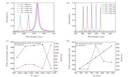
Fig. 3. (a), (b) Absorption spectra of different periods (Px and Py) based on a M-MoS2 perfect absorber. (c), (d) The relationship between the change in period and the absorption peak wavelength and quality factor(keeping other parameters unchanged).
It is well known that change in the period profoundly affects the frequency of the surface resonance mode of the metamaterial.[20-22]We will now explore the relationship between the absorption characteristics of the absorber in each period and the leakage rate (γe), as shown in Figs. 3(a) and 3(b). In Fig.3(a),whenPxchanges from 990 nm to 1110 nm,the absorbance about the resonance absorption peak first increases and then decreases, and the spectrum first undergoes a red shift and then a blue shift. In Fig. 3(b), the absorption peak trend aboutPyis consistent with that ofPx. When the periodPyincreases, the value of the resonant absorption peak first increases and then declines,and there is a significant red shift in the position of the absorption peak. Meanwhile,the perfect absorption state is reached whenPx= 1020 nm andPy=788 nm. In the whole process, the structure goes through three states of uncoupling,critical coupling and overcoupling. After determining the other geometrical structure parameters of the absorber and reaching the critical coupling state, we then show the functional relationship between the periodic change and the absorption peak wavelength andQfactor in Figs.3(c)and 3(d). WhenPxincreases,theQ-factor[=λ/full width at half maximum(FWHM)]of the system first increases,then decreases and finally increases again,while the absorption peak wavelength first increases and then decreases.Not only that,whenPyincreases,theQ-factor of the structure first increases and then decreases. In summary,the maximumQ-factor is 1256.8 for the periodPx=1110 nm,and the corresponding FWHM and resonance wavelength are 0.64 nm and 798.1 nm, respectively. The periodPy=788 nm has a maximumQ-factor of 828.8, and the corresponding FWHM and resonance wavelengths are 0.97 nm and 806.41 nm, respectively. The superiority of the designed system compared with previous work is in the better sensing performance of the absorber(Table 1).[23-27]

Table 1. Contrast with uniform type absorbers.
4. Conclusion
In general, we have obtained a perfect absorber with a M-MoS2structure. Meanwhile,the absorption characteristics simulated by the finite difference time domain method show that the absorption rate of the proposed MoS2-based absorber atλ=806.41 nm is as high as 99.8%. Our work also confirms,from both theoretical calculations and numerical simulations,that the reason for the perfect absorption of the ultranarrow band of M-MoS2is the strong limitation of the electromagnetic field by the critical coupling theory with guided resonance and suppression of the loss caused by reflection and transmission in the porous medium. By changing the structural parameters, the absorption spectrum can be moved in a wider wavelength range. At the same time, we also find that the maximumQ-factor of the structure is 1256.8 and the corresponding FWHM is 0.64 nm.Therefore,our research results may have important significance in the application of MoS2-based photodetectors, optical switches, modulators and many other photonic and optoelectronic devices.
Acknowledgments
Project supported by the National Natural Science Foundation of China (Grant Nos. 11604311, 61705204, and 21506257), the Scientific Research Fund of SiChuan Provincial Science and Technology Department, China (Grant Nos. 2020YJ0137 and 2020YFG0467), the National Defense Science and Technology Innovation Special Zone Project of China(Grant No.19-163-21-TS-001-067-01),and the College Students’s Innovation and Entrepreneurship Training Program(Grant No.S202110619065).
- Chinese Physics B的其它文章
- Measurements of the 107Ag neutron capture cross sections with pulse height weighting technique at the CSNS Back-n facility
- Measuring Loschmidt echo via Floquet engineering in superconducting circuits
- Electronic structure and spin-orbit coupling in ternary transition metal chalcogenides Cu2TlX2(X =Se,Te)
- Characterization of the N-polar GaN film grown on C-plane sapphire and misoriented C-plane sapphire substrates by MOCVD
- Review on typical applications and computational optimizations based on semiclassical methods in strong-field physics
- Quantum partial least squares regression algorithm for multiple correlation problem

