Impact of STI indium implantation on reliability of gate oxide
Xiao-Liang Chen(陈晓亮) Tian Chen(陈天) Wei-Feng Sun(孙伟锋) Zhong-Jian Qian(钱忠健)Yu-Dai Li(李玉岱) and Xing-Cheng Jin(金兴成)
1National ASIC System Engineering Research Center,School of Electronic Science&Engineering,Southeast University,Nanjing 210096,China
2China Resources Microelectronics Co.,Ltd,China
The impacts of shallow trench isolation(STI)indium implantation on gate oxide and device characteristics are studied in this work. The stress modulation effect is confirmed in this research work. An enhanced gate oxide oxidation rate is observed due to the enhanced tensile stress, and the thickness gap is around 5%. Wafers with and without STI indium implantation are manufactured using the 150-nm silicon on insulator(SOI)process. The ramped voltage stress and time to breakdown capability of the gate oxide are researched. No early failure is observed for both wafers the first time the voltage is ramped up. However, a time dependent dielectric breakdown (TDDB) test shows more obvious evidence that the gate oxide quality is weakened by the STI indium implantation. Meanwhile, the device characteristics are compared, and the difference between two devices is consistent with the equivalent oxide thickness(EOT)gap.
Keywords: silicon-on-insulator,shallow trench isolation(STI)implantation,gate oxide reliability
1. Introduction
Silicon on insulator(SOI)CMOS technology was first developed for military and space applications due to its intrinsic radiation hardening properties. Nowadays, SOI CMOS technology is also suitable for mixed signal,radio frequency(RF)and low power applications.[1]The SOI device is fully isolated by buried oxide and shallow trench isolation(STI).The absence of latch-up,reduced parasitic source and drain capacitances,and the ease with which shallow junctions are made are merely three obvious examples of the advantages presented by SOI technology over bulk.
Historically, SOI technology plays a critical role in the area of anti-single event effects in the radiation hush environment due to the thin silicon body.However,the damage caused by the total ionizing dose effect in the STI region and buried oxide interface remains a critical problem.[2,3]Previous studies show that the SOI body side-wall can form a parasitic transistor and the total irradiation dose effect has become the main factor in the production of large leakage currents in the STI region of SOI NMOSFETs.[4—9]
STI implantation is normally implemented to reduce the current leakage through the side-wall parasitic transistors. As shown in Fig. 1, the transfer characteristics of the STI parasitic transistor shift to the right side after STI sidewall implantation and the parasitic transistor is overwritten by the main device.[10]Indium is normally used due to the implant controllability and the low diffusion coefficient in silicon. However,the impacts of indium on the quality of gate oxide and device characteristics are rarely reported.

Fig.1. Transfer characteristics of a parasitic transistor.
2. Experimental details
2.1. Manufacture process
The devices researched in this work are manufactured using 150-nm SOI process technology. The process flow is similar to the normal deep sub-micron logic process. The difference is the substrate material: there is a buried oxide layer to isolate the top silicon. To begin this process,an STI structure,including STI implantation,is manufactured. In the follow-up process,impurity is implanted to form well isolation and to adjust the threshold voltage,respectively. Then,an oxide film is grown using a dry oxidation process at 800°C and it is used as a gate dielectric. Poly silicon film is deposited as the gate material. After gate patterning and etching, a light-doped drain(LDD)and heavy doped source/drain are implanted. Once the front end of the line process is finished,the co-silicide film is formed for low resistive contacts. The metallization process is totally compatible with the logic process.
The detailed STI formation process is explained below for a thorough understanding of this research. The isolationtrench is etched first using a blocked hard mask technology,where the pad nitride film is used. An STI liner oxidation process is carried out to eliminate the silicon damage induced by etch plasma. Next,STI indium implantation is executed to increase the threshold voltage(VT)of the parasitic transistor. A structural diagram of STI implantation is shown in Fig.2;the indium dose varies from 0 to 8×1013cm−2in this work. It is worth noting that most of the area of the wafer is covered by the pad nitride film during STI implantation,and the thickness is about 1000.STI is then filled up with high density plasma(HDP)oxide and followed by a thirty second anneal at a temperature of 1050°C.After removing the unwanted HDP oxide using an STI chemical mechanical polish(CMP)process,the pad nitride mentioned above is striped chemically.

Fig.2. A structural diagram of STI implantation.

Fig.3. The layout structure of the capacitor.
2.2. Test structure and method
Analysis of the oxide quality is performed via the measurement of capacitors,the layout of which is shown in Fig.3.The capacitor is surrounded and isolated by an STI ring. A T-shaped poly-silicon gate is used as one of the capacitor electrodes. Body, source and drain terminals are tied together as the other capacitor electrode. The grown gate oxide is the dielectric film. The area of the capacitor is 5×10⁻⁴cm−2.Besides the equivalent oxide thickness (EOT) measurement of the dielectric film, two types of reliability evaluation are implemented in this research. First, the early life failure of gate oxide is evaluated using the ramped voltage breakdown method. Second, the long term reliability is evaluated using the charge to breakdown method (TDDB). The nominal 5-V I/O transistors are also tested. The characteristics of the transistors, such as the threshold voltage,I—Vcurve and subthreshold slope,are reviewed to evaluate the impact of indium implantation.
3. Results and discussion
3.1. Film stress after indium implantation
According to the theory of stress memorization technique(SMT),the stress of silicon nitride can be modulated by dopant implantation of large ions that have a molecular weight greater than or equal to silicon. The tensile stress of nitride film can be improved up to 60% compared to the film without dopant implantation.[11,12]To confirm this,the radius of curvature was measured for the wafers prior to and post indium implantation.
Figure 4 compares the radius of the curvature of the wafers for various indium dosages. It can clearly be seen in this chart that the radius of curvature is reduced for all the indium implantation conditions. This indicates the increasing film strain. We can also see in this chart the decreasing trend of the radius as the indium dosage increases. These results confirm that the tensile stress is strongly associated with indium impurity dosage, and this is consistent with the stress modulation theory.

Fig.4. Comparison of the radius of curvature.
3.2. Impact of STI indium implantation on oxidation rate
In this experiment,STI implantation is skipped for wafer#2 and #3, and an indium dosage of 5×1013cm−2is implanted in wafer #1 and #4. The physical thickness is measured immediately using an optical measurement system after the gate oxidation process. The thickness comparison of gate oxide is shown in Fig. 5. It can be observed that gate oxideis about 5% thicker for the wafers with indium implantation.The thickness difference is also supported by TEM,as shown in Fig.6. However,there is a gap between spectroscopic ellipsometry and TEM. One reason for this is the oxide regrowth during dual gate oxidation and the annealing process;another possible reason is the fixed offset between the two measurement methods induced by system setting. Nevertheless, the difference introduced by the indium dose is confirmed.

Fig.5. The impact of STI implantation on oxide thickness.

Fig.6. TEM images to confirm oxide thickness.
The EOT of gate oxide is measured to confirm the impact of indium on electrical properties. Figure 7 reveals that there is an obvious increase in the EOT.The EOT increases linearly from 158to 164as the indium dosage varies from zero to 8×1013cm−2.
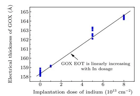
Fig.7. The EOT of oxide trend with the indium implantation dose.
It can be deduced that the oxidation rate is enhanced by indium implantation and it is sensitive to implant dosage. This phenomenon can be explained by the model of the stress effect on the oxidation rate.[13]Figure 8 illustrates the impact of tensile stress on a silicon surface. The silicon atoms are pulled off their initial position and mismatches of the silicon lattice are generated. After the HDP annealing process, the tensile stress is transferred to the silicon surface and is memorized by the silicon lattice. Therefore, the impact of the tensile stress on the silicon lattice will not disappear,even when the nitride film is removed after STI CMP.

Fig.8. A structural diagram of the stress impact on silicon.
A widely used relationship between the thicknessLof an oxide layer and oxidation timetat a constant temperature is the linear—parabolic equation[13]

in whichAandBare parameters that are not dependent on thickness and time.
A variety of independent researchers have confirmed that parameterBis related to the diffusion coefficientDof the oxidant through the oxide:[14—16]

in whichCLis the concentration of molecular oxygen or water dissolved in the silicon at the silicon—gas interface andρis the density of oxide in the same concentration units. Strain in the oxide layer influences the molecular diffusion of oxygen or water in the layer:

whereDLis the diffusion coefficient when there is no strain,kis a parameter measuring the sensitivity of the diffusion coefficient to strain andεis the strain in the oxide layer.
Normally, the grown silicon oxide film is compressively strained due to the fact that the molecular weight of oxide is greater than silicon. However, due to the tensile stress transferred from the nitride layer, stress compensation occurs and the compressive stress of the silicon oxide film is decreased.The diffusion coefficient of oxygen is higher compared to thewafers with no STI implantation, as Eq. (3) expressed. According to Eqs. (1) and (2), it can be deduced that the thickness of silicon oxide is higher for the indium-implanted wafer under the same oxidation process conditions.
3.3. Impact of implantation on oxide quality
Gate oxide breakdown has been an important reliability issue for modern MOS devices. It is widely believed that defects and mismatches generated within the oxides are responsible for the breakdown and many other reliability issues.[17,18]Research results show that the high-field traps with a size of 10−14cm2possess all the characteristics required for breakdown and play a dominant role. Degradation and breakdown have a common physical origin and were attributed to the defect band formation in the oxide under electric stress.[19,20]
The early life failure of gate oxide is evaluated using ramped voltage breakdown measurement. A negative voltage bias sweep of 100 V·s−1is applied to the gate terminal.Breakdown is defined as the point at which 1 µA of current flowed through the oxide. The full-map data are collected for both wafers,with and without STI implantation,and they are shown in Fig.9.The unit is the Volt.It can be observed that no early breakdown occurred for both wafers. This means there are no oxide integration issues induced by STI implantation.However,the value of the breakdown voltage of the wafer with an indium implant is 0.4 V to 0.6 V higher than that without implantation due to the thickness difference mentioned above.
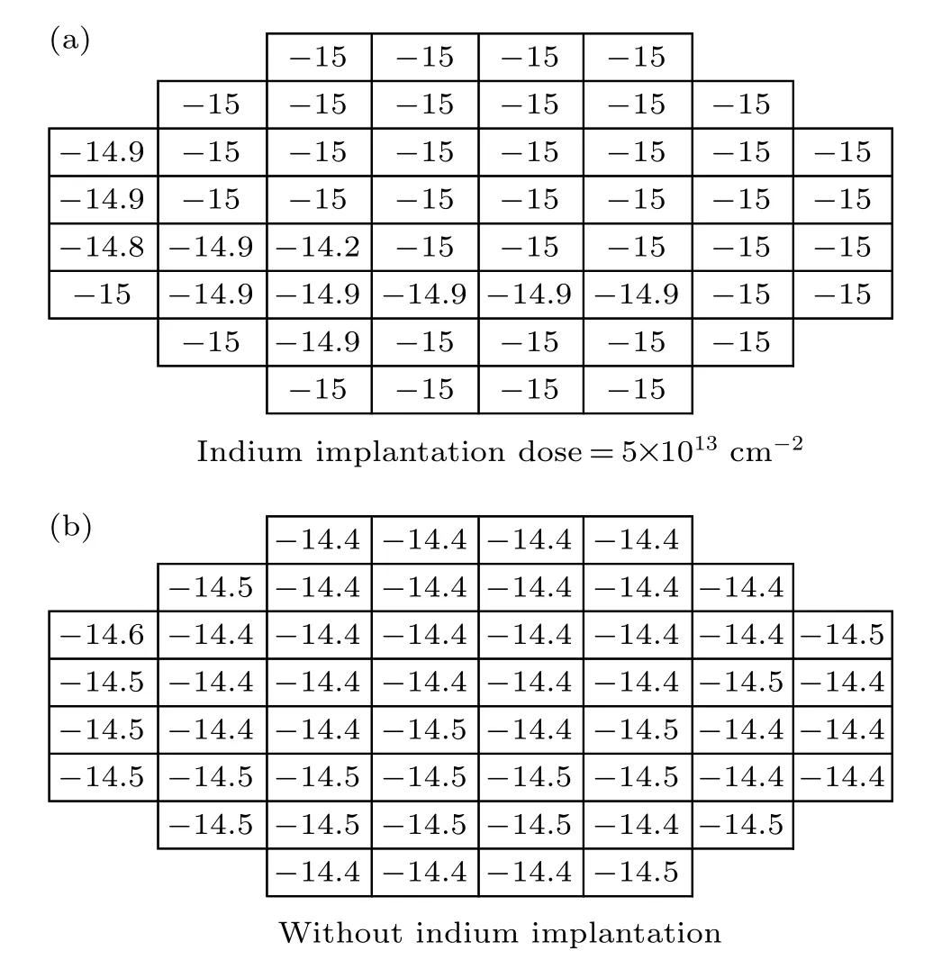
Fig.9. A wafer map of ramped voltage breakdown.
Figure 10 shows the similarI—Vcharacteristics for both wafers, with and without indium implantation. The leakage begins to increase at around 10 V.However, there is an obvious shift in the wafer with indium implantation. The shift of the voltage is around 5%, which is consistent with the difference in the dielectric thickness. The observed correlation between theI—Vcurve and oxide thickness might be explained by the theory of F—N tunneling, which is strongly correlated with the electric field across the dielectric.[21]These results provide further support for the hypothesis that the oxide thickness is physically increased by indium implantation.
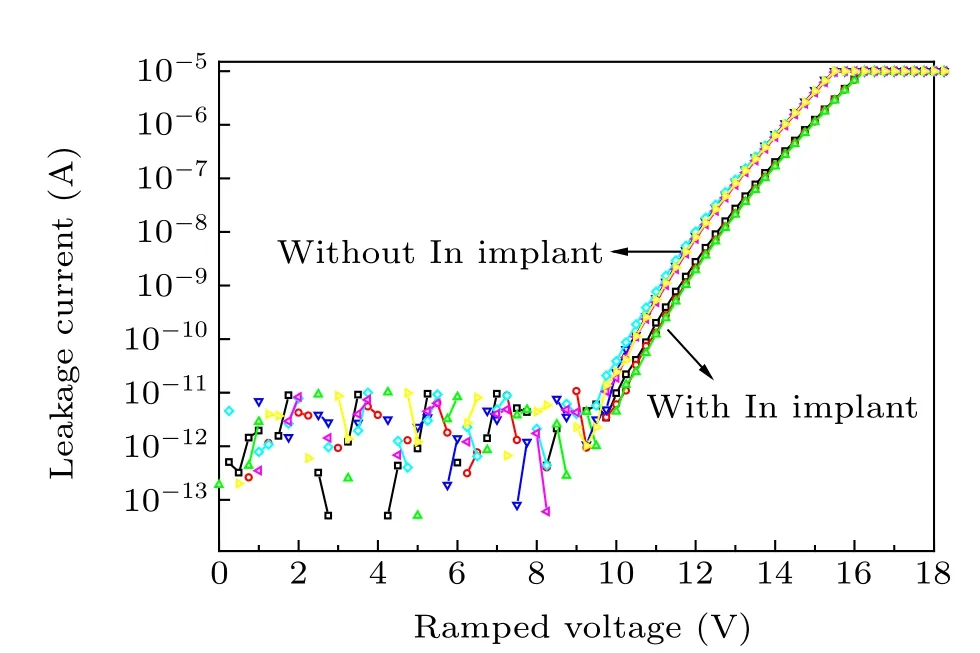
Fig.10. Comparison of I—V characteristic.

Fig.11. A wafer map of time to breakdown.
Long term reliability of gate oxide is evaluated using TDDB.Gate oxide capacitors are subjected to a constant current stress with a current of 50 nA; the sign of the current is chosen to ensure that the underlying silicon is in accumulation mode. Time to breakdown is defined as the point at which the voltage across the oxide drops to lower than 10 V.The time to breakdown is measured for both wafers and the full-map data are collected in Fig.11. The TDDB characteristics are shown in Fig.12.
The maximum time is set as 99 s during the test. It can be observed from the result that no breakdown occurs in the wafer without indium implantation. However, time to breakdown is relatively lower in the wafer with indium implantation. This can be explained by the existence of defects and lattice mismatches on the silicon surface due to the enhanced tensile stress analyzed above.
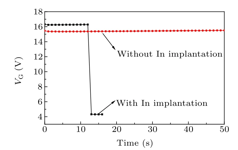
Fig.12. TDDB test characteristics comparison.
Interestingly,the reliability data show that only TDDB is affected by indium implantation. No ramped voltage breakdowns occurred. A possible explanation for this might be that the initial defects induced by indium are very small particles or structural weakness, as shown in Figs. 13(a) and 13(b).These defects will not induce breakdown as there is no current path under ramped voltage stress. However, as shown in Fig. 13(c), the small defects or structural weakness grow to become cluster defects under the TDDB stress. Breakdown occurs once the cluster defect punches through the whole dielectric,as Fig.13(d)shows.
Although there is no failure under the ramped voltage stress, the indium impact can still be observed if we repeat the ramped voltage stress several times. The wafer with indium implantation showed failure after two or three cycles of voltage ramp-up. However,this was not the case in the wafer without indium implantation. This finding also supports the association between indium implantation and gate oxide quality.

Fig.13. A diagram of dielectric breakdown
3.4. Impact on the transistor characteristics
The impacts of indium implantation on transistor characteristics are also reviewed. Table 1 provides a summary of the electrical statistics of the two devices. Both the threshold voltage and sub-threshold slope of the wafer without the indium dose are about 5%lower than the other. This is matched with the EOT difference. Figures 14 and 15 present the transfer characteristics and theI—Vcurves of the two transistors,respectively. From Fig. 14, we can see there is a shift in the linear region,and this is reasonable when considering the EOT difference induced by indium implantation. In Fig.15,the saturation current difference between the two devices can also be explained by the EOT gap. Non-saturatedIDbehavior can be observed whenVGis lower than 5 V.This can be explained by the“kink”effect,which is induced by the high electrical field at the drain end. This is common in SOI devices.

Table 1. A summary of the electrical parameters of the device.

Fig.14. Comparison of NMOSFET transfer characteristics(VD=0.1 V).
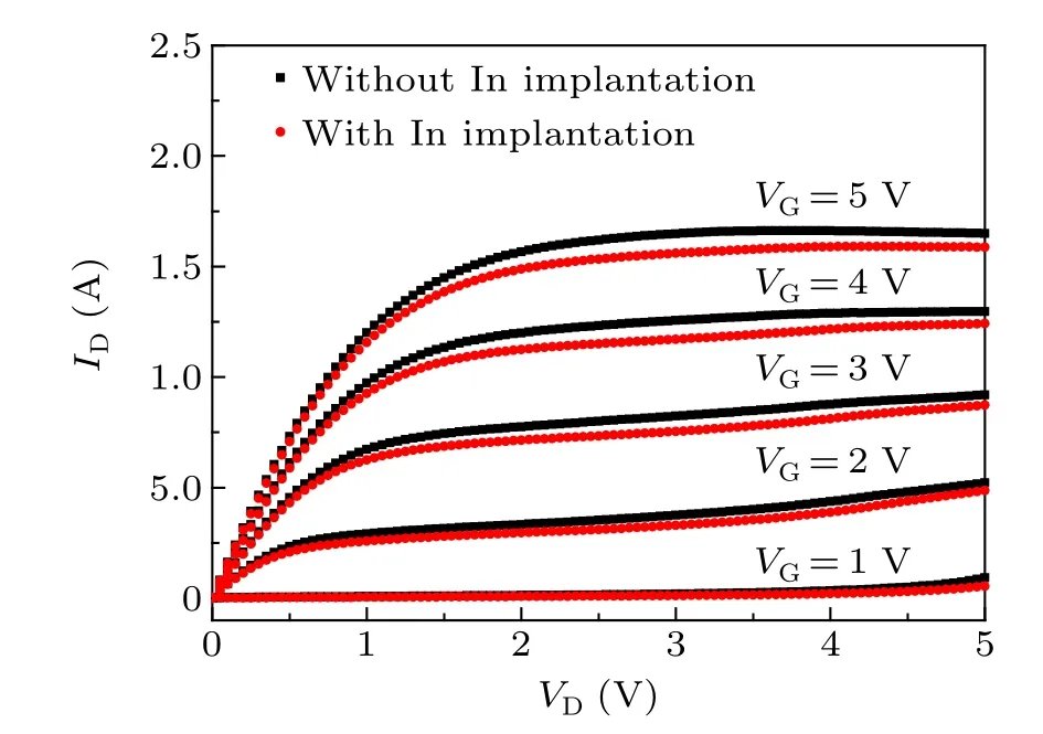
Fig.15. NMOSFET VD—ID characteristics comparison.
4. Conclusion and perspectives
The impacts of STI indium implantation on gate oxide quality and transistor characteristics are studied in this work.The study has confirmed the stress modulation effect induced by indium implantation. The research has also shown that the oxidation rate is increased by the strain compensation induced by STI indium implantation. The thickness gap is confirmed by both TEM and EOT measurement. The results of this study show that the gate oxide quality is weakened by STI indium implantation. Early failure of gate oxide is measured using the ramped voltage breakdown method. Although there is no early failure the first time the voltage is ramped up, the impact of the indium dose can be observed after repeating the stress several times. However, the more obvious impact can be observed from long term reliability analysis,evaluated using time to breakdown measurement. The results of this study indicate that the intrinsic defects or structural weakness are introduced by the stress modulation effect. This paper provides a comprehensive explanation based on the stress modulation theory and defects growth model. This study is limited by the lack of information on the direct measurement of silicon defects or lattice mismatch. Further research should be undertaken to explore the links between indium dosage and silicon defects more closely.
Although indium implantation is good at profile controllability, the results, however, indicate that indium decreases the gate oxide reliability and is not the appropriate dopant for STI implantation for TID hardening. To improve gate oxide reliability,the spices with fewer stress modulation effects,such as B and BF2, would be a better choice. However, further study should be focused on implantation conditions and thermal budget optimization for better dopant profile control.
- Chinese Physics B的其它文章
- High sensitivity plasmonic temperature sensor based on a side-polished photonic crystal fiber
- Digital synthesis of programmable photonic integrated circuits
- Non-Rayleigh photon statistics of superbunching pseudothermal light
- Refractive index sensing of double Fano resonance excited by nano-cube array coupled with multilayer all-dielectric film
- A novel polarization converter based on the band-stop frequency selective surface
- Effects of pulse energy ratios on plasma characteristics of dual-pulse fiber-optic laser-induced breakdown spectroscopy

