Electrically-manipulable electron-momentum filter based on antiparallel asymmetric double δ-magnetic-barrier semiconductor microstructure∗
Ge Tang(唐鸽) Ying-Jie Qin(覃英杰) Shi-Shi Xie(谢诗诗) and Meng-Hao Sun(孙梦豪)
1College of Science,Shaoyang University,Hunan 422004,China
2College of Science,Guilin University of Technology,Guilin 541004,China
Keywords: magnetic microstructure,bias,wave vector filtering(WVF)effect,electrically-tunable momentum filter
1. Introduction
Advanced modern materials growth techniques (such as molecular beam epitaxy) make it possible to confine the motion of high mobility two-dimensional electron gas (2DEG)in a modulation-doped semiconductor heterostructure by an inhomogeneous magnetic field,[1]e.g., patterning a ferromagnetic (FM) stripe on the surface of GaAs/AlxGa1−xAs heterostructure,[2]which allows to construct so-called magnetic microstructure in experiments.[3]In fact, magnetic microstructure consists of magnetic materials and semiconductor, where the former produces an inhomogeneous magnetic field affecting locally the motion of electrons in latter. Because of small size, low dimensionality and quantum magnetic confinement,some novel quantum effects exist in the magnetic microstructure,[4]e.g., wave-vector filtering(WVF),[5]magnetoresistance (MR) effect[6–9]and electronspin polarization.[10–13]Meanwhile,these effects can be used to develop new nanoelectronics devices.[14–16]
Recently,WVF effect in magnetic microstructure has attracted much interest, owing to its scientific importance[17]and potential application.[18]Physically,such an effect results from an essentially two-dimensional (2D) process for electrons across magnetic microstructure.[5]In 2017,Luet al.[19]firstly reported a theoretical study on WVF effect and its control viaδ-doping in an experimentally-realizable magnetic microstructure. They found a considerable WVF effect,and confirmed that WVF efficiency can be controlled structurally byδ-doping. Since then, WVF effect in magnetic microstructures was explored extensively and corresponding electronmomentum filters were proposed successfully.[20–24]
More recently, an idea to confine 2DEG motion by an electric field, e.g., patterning Schottky-metal (SM) stripe on semiconductor heterostructure,[25,26]is put forward, in order to enhance manipulation to electron-momentum filter based on the magnetic microstructure. By depositing a FM stripe and a SM stripe on the top and the bottom of GaAs/AlxGa1−xAs heterostructure,respectively,Liuet al.[27]found that this kind of magnetic microstructure also possesses an appreciable WVF effect and its efficiency can be altered by SM stripe. Ulteriorly, manipulating WVF effect byδ-doping and applied bias was investigated independently by Liuet al.[28]and Konget al.,[29]respectively. Very recently, WVF effect[30]and influence ofδ-doping[31]as well as applied bias[32]were studied in another such magnetic microstructure,where a FM stripe and a SM stripe were patterned,in parallel configuration,on the surface of GaAs/AlxGa1−xAs heterostructure. These works not only revealed general rule of electric field controlled WVF effect in such magnetic microstructures, but also proposed the electrically-controllable electron-momentum filter for nanoelectronics device applications. By applying a bias, in the present work, we explore electric control to WVF effect for electrons in a magnetic microstructure,aiming at developing a new electrically-controllable electron-momentum filter for nanoelectronics device applications.
2. Model and method
We consider a magnetic microstructure[33]as plotted briefly in Fig. 1(a), where two asymmetric FM1and FM2stripes are patterned on the top and the bottom of GaAs/AlxGa1−xAs heterostructure,[34]respectively,and structural model is presented in Fig. 1(b). When vertical distance between FM stripes and 2DEG plane is very small as well as conductivity is identical everywhere within 2DEG, horizontally magnetized FM stripe induced magnetic fields and applied negative voltage(−Vg)produced electric potential can be viewed as[35]delta-function magnetic-barrier (MB) and rectangular electric-barrier(EB),respectively,i.e.,

whereδ(x) is Dirac delta-function,B1,2stands for magnetic strength of twoδ-MBs,U0represents EB height, andLis structural width or separation between twoδ-MBs.
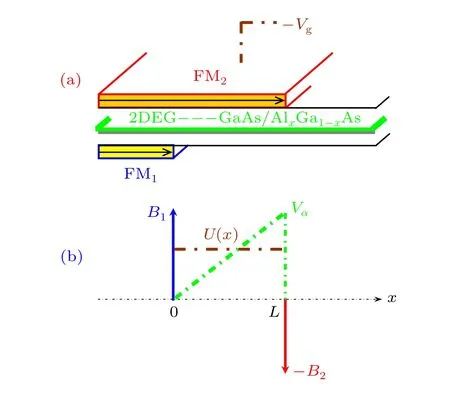
Fig.1. (a)Magnetic microstructure and(b)its structural model with a bias.
At the presence of a bias(Vα),the Hamiltonian describing an electron in such a magnetic microstructure can be written,in the framework of single particle,effective mass approximation,by[36]
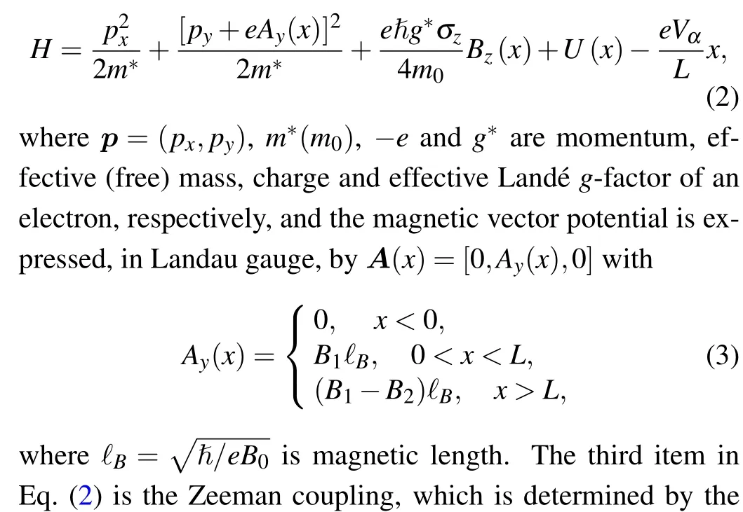

For a magnetic microstructure, electron is free along they-direction, solution of its stationary Schr¨odinger equation,HΨ(x,y)=EΨ(x,y), can be therefore written by Ψ(x,y)=ψ(x)exp(ikyy),whichkyis wave vector iny-direction andxcomponent of wave functionψ(x)complies with reduced onedimensional(1D)Schr¨odinger equation

Clearly,thisUeffdepends not only on wave vector(ky),but also on bias(Vα). It isky-dependence ofUeffthat renders an essentially 2D-process for electrons across a magnetic microstructure, leading to a WVF effect. TheVα-dependentUeffmakes possible control of WVF effect by an applied bias in a magnetic microstructure based electron-momentum filter.

3. Results and discussion
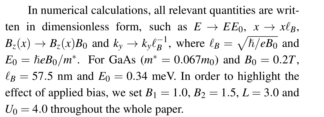
We start with transmission coefficient for electrons traversing our considered magnetic microstructure. Figure 2 shows variation of transmission coefficient (T) with incident

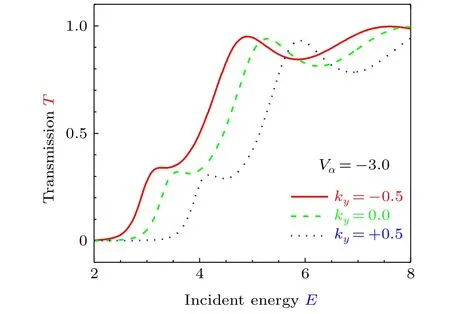
Fig.2. Transmission coefficient changes with incident energy for different wave vectors and a fixed bias.
In Fig.3,we present WVF efficiency(η)versus incident energy(E)for a fixed wave vectorky=0.0(i.e.,the normal incidence)and several concrete applied biases:Vα=1.0(solid line),2.0(dashed line)and 3.0(dotted line),respectively. One can observe from this figure that WVF efficiencyηwill be greatly altered if applied biasVαchanges. For considered energy range,WVF efficiency decreases obviously and its curve shifts to low-energy direction. Clearly,modulation of applied bias(Vα)to WVF effect stems fromVα-dependence of effective potentialUefffelt by electrons in magnetic microstructure.
In order to observe the modulation of applied bias on WVF effect more intuitively, in Fig. 4 we directly present change of WVF efficiency(η)with applied bias,where wave vector is still set to beky=0.0,but incident energy is chosen asE=2.0 (solid curve), 5.0 (dashed curve) and 8.0 (dotted curve), respectively. Indeed, it is true from this figure that an applied bias impacts on the WVF effect for electrons in the magnetic microstructure. Both magnitude and sign of WVF efficiency are dramatically altered with applied bias. Furthermore, the impact of an applied bias on WVF effect is related closely to incident energy,especially for incident energyE=5.0(see green line). Actually,influence of an applied bias to WVF effect attributes to the dependence of effective potential felt by electrons in the magnetic microstructure on the applied bias[cf. Eq.(5)],which makes possible the control of electron-momentum filter (see Fig. 1) by an applied bias and gives rise to an electrically-tunable electron-momentum filter.

Fig.3. WVF efficiency varies with incident energy under applied bias.

Fig.4. WVF efficiency varies with incident energy under applied bias.
So far, the results are obtained only for one wave vector(ky=0.0). In order to observe the control of an applied bias to considered electron-momentum filter for different wave vectors,finally,Fig.5 plots the WVF efficiency(η)as a function of applied bias (Vα), where three wave vectors are taken into account:ky=−0.5 (solid line), 0.0 (dashed line) and +0.5(dotted line),while incident energy is fixed atE=5.0 for simplicity. From these(η–Vα)curves,we can see evidently that,an applied bias creates non-identical influence for different wave vectors on WVF effect for electrons to tunnel through the magnetic microstructure, especially at the case ofky=+0.5.Such a difference originates from the dependence of effective potential (Ueff) experienced by electrons in the magnetic microstructure on wave vector(ky)[see Eq.(5)].Thus,an applied bias does impact on WVF effect in the magnetic microstructure for all of wave vectors.
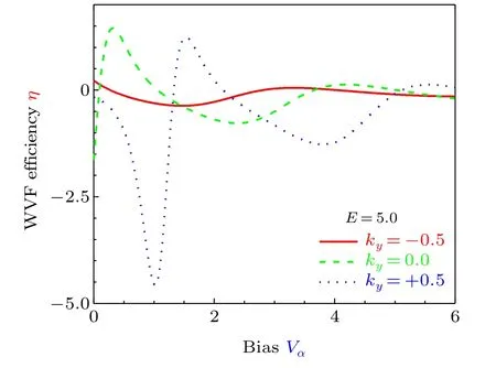
Fig.5. WVF efficiency changes with applied bias for different wave vectors and fixed incident energy.
4. Conclusions
To sum up, control of WVF effect via an applied bias is investigated theoretically for electrons in a magnetic microstructure,which can be realized experimentally by depositing two asymmetric FM stripes on the top and the bottom of GaAs/AlxGa1−xAs heterostructure,respectively. An appreciable WVF effect is revealed in such a magnetic microstructure under a bias, which attributes to an essentially-2D process for electrons across a magnetic microstructure,regardless of whether or not a bias is applied. Moreover, both magnitude and sign of WVF efficiency can be tuned by changing an applied bias, which may lead to an electrically-manipulable electron-momentum filter for nanoelectronics device applications.
- Chinese Physics B的其它文章
- Physical properties of relativistic electron beam during long-range propagation in space plasma environment∗
- Heterogeneous traffic flow modeling with drivers’timid and aggressive characteristics∗
- Optimized monogamy and polygamy inequalities for multipartite qubit entanglement∗
- CO2 emission control in new CM car-following model with feedback control of the optimal estimation of velocity difference under V2X environment∗
- Non-peripherally octaalkyl-substituted nickel phthalocyanines used as non-dopant hole transport materials in perovskite solar cells∗
- Dual mechanisms of Bcl-2 regulation in IP3-receptor-mediated Ca2+release: A computational study∗

