Dual-wavelength ultraviolet photodetector based on vertical(Al,Ga)N nanowires and graphene*
Min Zhou(周敏) Yukun Zhao(赵宇坤) Lifeng Bian(边历峰) Jianya Zhang(张建亚) Wenxian Yang(杨文献)Yuanyuan Wu(吴渊渊) Zhiwei Xing(邢志伟) Min Jiang(蒋敏) and Shulong Lu(陆书龙)
1Suzhou Institute of Nano-Tech and Nano-Bionics(SINANO),Chinese Academy of Sciences(CAS),Suzhou 215123,China
2School of Nano-Tech and Nano-Bionics,University of Science and Technology of China,Hefei 230026,China
Keywords: dual-wavelength ultraviolet photodetector,(Al,Ga)N nanowire,graphene,molecular beam epitaxy
1. Introduction
In recent years, due to a wide range of applications in communication, flame sensors, ozone monitoring, and even ultraviolet (UV) astronomy, people have great interest in UV-A (320 nm-400 nm) and UV-C (200 nm-280 nm) photodetectors.[1,2]By reducing false positive detection, dual-wavelength photodetectors are beneficial to increase accuracy.[3]In general, measuring dual-wavelength bands typically requires double detectors with separate cooling assemblies and readout circuits.[3,4]However,it could increase the manufacturing costs and enhance the difficulties of assembling double different detectors.[3,5]A single photodetector responding in dual wavelengths paves an efficient way to overcome the above problems.[3]For example, dualwavelength detection can clearly distinguish the missile from its plume and can reduce mine detection errors.[3]Hence,dualwavelength (UV-A/UV-C) photodetectors are necessary and promising for future markets of UV detections.
Due to the continuous adjustable bandgap covering the range from about 200 nm to 365 nm,(Al,Ga)N can shield the interference of visible light without any special filters compared with Si.[6-10]Thus, (Al,Ga)N is beneficial for detector miniaturization and saving the cost of filters. In addition to the extraordinary characteristics of being nontoxic, long lifetime and high stability against UV radiation, (Al,Ga)N is an ideal material for making UV photodetectors.[6-9,11]Moreover, compared with thin films or bulk, nanowires show better photoelectric properties due to its large specific surface area and smaller size.[12-14]Nanowires have special ability for selectively enhancing nanoscale light absorption due to their optical properties.[15]However, to date, most UV detectors are based on thin films or bulk materials, and few groups have studied UV detectors based on vertical(Al,Ga)N nanowires.[16,17]In our previous work,a UV detector based on(Al,Ga)N nanowires only achieved a single response in the UV range.[16]The results agree with those from another group.[17]The underlying mechanism is still unclear. Therefore, it is promising but highly challenging to achieve dual-wavelength UV photodetectors based on vertical(Al,Ga)N nanowires.
In this work, we demonstrate a dual-wavelength (UVA/UV-C) detector based on (Al,Ga)N/GaN nanowires. The dual-wavelength detector provides double responses in UVA and UV-C regions. The maximum responsivity of UV-C band is over 15.5 mA·W-1, while that of UV-A band is over 5.0 mA·W-1. Due to the good transparency and conductivity,graphene is utilized as a current collecting layer. The underlying mechanism contributing to the double responses has been studied systematically.
2. Experiments
Vertical(Al,Ga)N nanowires were grown on Si substrate by molecular beam epitaxy(MBE).Prior to the MBE growth,the Si(111)substrate in the growth chamber should be heated up to about 900°C for 15 min to eliminate the native oxides.The 7×7 reconstruction was normally observed after this treatment,indicative of a clean surface.Initially,an AlN buffer layer was grown with a nominal Al flux of~3.0 nm·min-1for 1.0 min. Subsequently,GaN nanowires were grown with a Ga flux of~3.0×10⁻⁸Torr for about 100 min with a growth rate of~3.8 nm·min-1. The substrate temperature is set to be 770°C.The deposited GaN initially forms into islands which act as a material collector and a seed for the nanowires.[16]After the growth of GaN section,the(Al,Ga)N section was grown for 90 min with a constant substrate temperature of 770°C.Two thin AlN sections were inset into the(Al,Ga)N section as mark layers. When start and finish growing the(Al,Ga)N segment,the shutters of Al and Ga cells were opened and closed simultaneously by the software. To increase the nanowire uniformity,samples were rotated with a rate of 120°/s during the growth process.
To fabricate the photodetectors,a thick SiO2film was deposited on the surface of nanowires. Then some parts of the SiO2film were removed to form a square area to expose some nanowires. After that, Ti/Al (50/200 nm) was deposited as a backside electrode on the backside of the Si substrate by electron beam evaporation. Ohmic contact is formed by annealing at 400°C in N2atmosphere for 30 min. Graphene was transferred to the top of the nanowires by wet transfer as a transparent current collecting layer.[18]The transfer process is shown in Fig. SI (supporting information). Finally, Ti/Pt/Au(25/55/300 nm) was deposited on the graphene surface as an electrode.
Scanning electron microscopy(SEM),scanning transmission electron microscopy(STEM)and high-resolution energy dispersive x-ray (EDX) mapping were used to characterize the surface morphology and element distribution of nanowires.The STEM samples were prepared by focused ion beam(FIB).The intrinsic emission spectra of (Al,Ga)N nanowires were measured by photoluminescence (PL). The current-voltage and transient responses characteristics of the (Al,Ga)N photodetectors were measured by the probe station. The spectral response measurement employed a self-constructed photoelectric measurement system mainly consisting of an optical chopper, a xenon lamp, a data processing center and a power supply.
3. Results and discussion
From the top-view and side-view SEM images in Fig. 1(a), the vertical nanowires are formed and distributed on the Si substrate with good verticality and small fluctuation.As shown in Fig. 1(b), vertical (Al,Ga)N sections have been fabricated as designed. The lateral surface of GaN segment is wrapped by (Al,Ga)N section, forming a core-shell structure. Fig. 1(c) illustrates element distribution from the top to bottom regions of a nanowire,which further demonstrates the existence of(Al,Ga)N section.
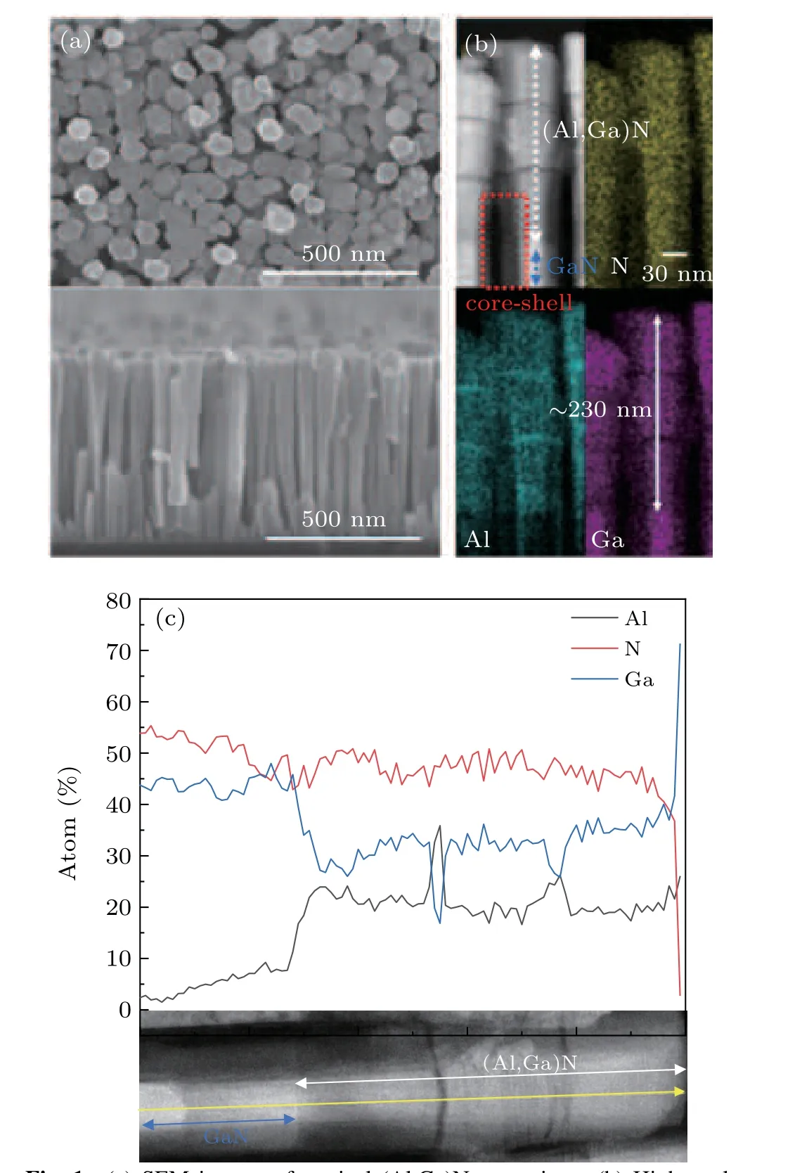
Fig. 1. (a) SEM images of vertical (Al,Ga)N nanowires. (b) High angle annular dark field STEM images of vertical(Al,Ga)N nanowires. (c)Highresolution EDX mapping analysis about the element distributions of vertical(Al,Ga)N nanowires.
The PL spectra of (Al, Ga)N nanowires are shown in Fig. 2(a).Eg(AlN) andEg(GaN) are the bandgap of AlN and GaN at room temperature, which are 6.2 eV and 3.4 eV,respectively,[19,20]

According to Eq.(1),the Al content is calculated to be about 18%.[21]As the Raman spectrum shown in Fig.2(b),three obvious peaks exist, namely D peak, G peak and 2D peak. G peak(~1581 cm-1)is caused by the in-plane vibration of sp2hybrid carbon atoms,which proves the existence of graphene after fabricating detectors.[16]D peak (~1343 cm-1) is related to graphene defects[22]and the 2D peak(~2693 cm-1)in graphene is due to two phonons resonance.[23]The number of graphene layers is reflected by the ratio of 2D peak intensity to G peak intensity(I2D/IG).By calculating,the ratioI2D/IGis 0.56,indicating that graphene has a multilayer structure.[24,25]TheI-Vcharacteristics of the detector under dark,UV-A and UV-C illumination (at 254 nm and 365 nm, corresponding to AlGaN and GaN band edge, respectively) were measured by Agilent B1505A instrument for observing the rectification and photo response characteristics. As shown in Fig. 2(c), theIVcurves of the detector under no illumination are nonlinear,which indicates that Schottky contact exists between graphene and nanowires.[26]In addition,under 254 nm and 365 nm illumination, the asymmetry is more obvious relative to the bias direction,indicating that the detector has good response characteristics to UV-C and UV-A illumination. Furthermore,the dark current of the detector is 34.6 nA at-2 V with an area of 0.96 mm2.
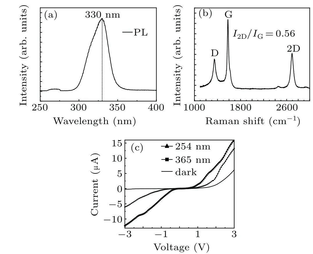
Fig. 2. (a) PL spectrum of vertical (Al, Ga)N nanowire array. (b) Raman spectrum of the graphene film measured with an excitation wavelength of 532 nm. (c) Current-voltage characteristics of detector in dark, UV-A and UV-C illumination measured at room temperature.
Figure 3(a)shows a schematic diagram of the detector under the measurement of responsiveness. When testing responsiveness,a bias of-2 V is applied to the detector.The spectral responsivity of the detector is defined as the photocurrent output under the action of the unit incident radiation power.[27]As shown in Fig. 3(b), the black triangle represents the experimental data,and the red line represents the data smoothed by 12 points. It is clearly illustrated that the detector shows a dual-wavelength response in the band of 240 nm-400 nm.The maximum responsivity of the first response in the range of UV-C band exceeds 15.5 mA·W-1, while that of the second response in the range of UV-A band is over 5.0 mA·W-1.The rejection ratio (R254nm/R450nm) exceeds 35 times at an applied bias of-2 V.
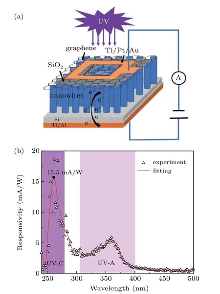
Fig.3. (a)Schematic diagram of detector. (b)Spectral response of the detector at the bias at-2 V.
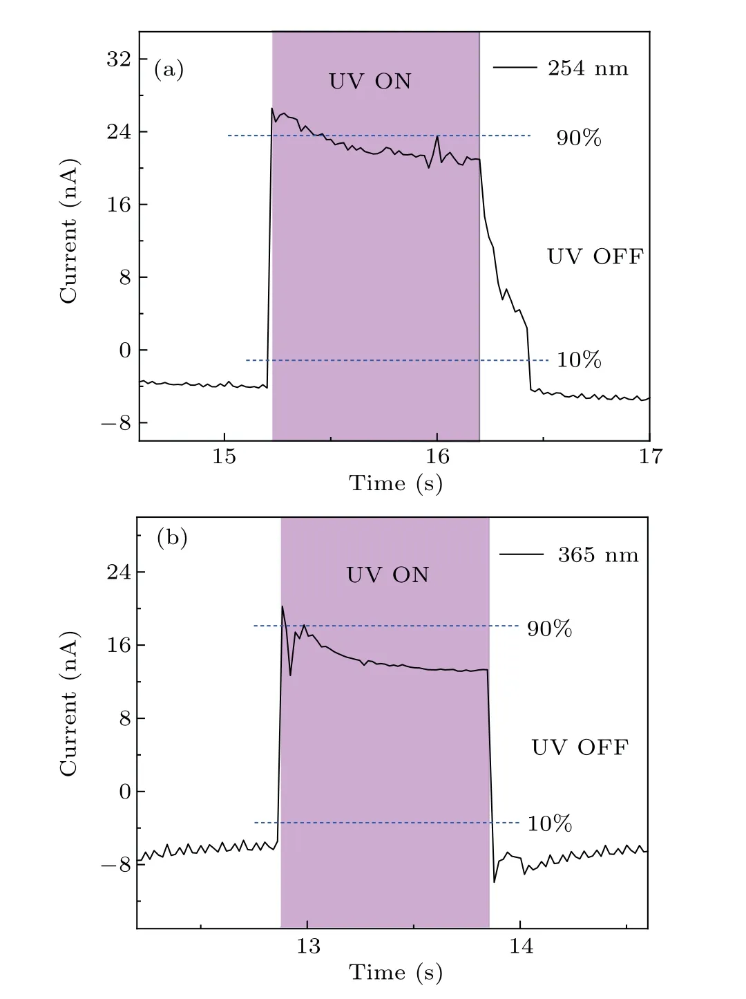
Fig.4. (a)Transient response of the detector to 254 nm(UV-C)illumination.(b)Transient response of the detector to 365 nm(UV-A)illumination.
Figures 4(a) and 4(b) show the current switching characteristics of the detector under UV-C (254 nm) and UV-A(365 nm)illumination at-2 V,corresponding to the first and the second responses,respectively. The on/off current can increase/decrease in a certain period of time with/without UV irradiation. All measurements have been conducted at room temperature in air. The rise time (defined as the time when the current rises from 10%to 90%of the peak current value)is less than 20 ms and 20 ms and the decay time (defined as the time when the current drops from 90% to 10% of the peak current value) is less than 960 ms and 955 ms under 254 nm and 365 nm illumination, respectively. The accuracy of our equipment is 20 ms. By comparing the key parameters listed in Table 1, graphene/AlGaN /GaN nanowires has advantages in transient response compared with some recent new photodetectors.[28-33]
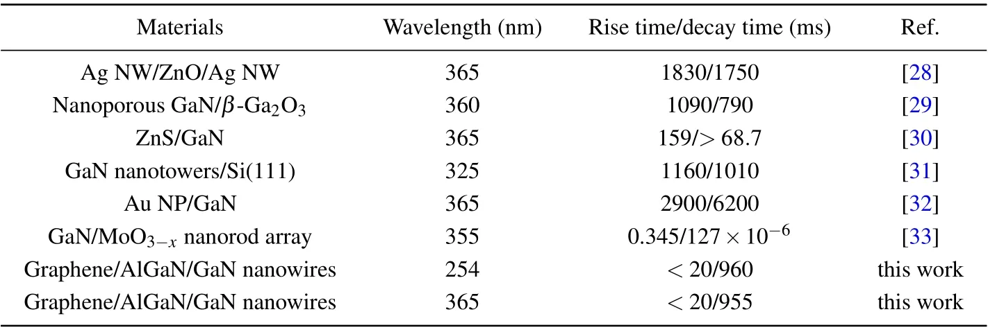
Table 1. Comparison of response time between this work and some state-of-the-art reports.
In order to further study the underlying mechanism of dual-wavelength UV detector,we plot the schematic diagrams in Fig.5. At-2 V bias voltage, when UV light irradiates on the photodetector(Fig.5(a)),photons can reach the nanowires through the graphene as it is thin enough and transparent in the UV range. Then, photons can be absorbed by (Al,Ga)N and GaN sections, producing electron-hole pairs. Due to the core-shell structure of nanowires,there are two ways(Fig.5(a)1 and 2) for photogenerated carriers to diffuse to the electrodes. “1” in Fig. 5(a) indicates the common way, and carriers are diffused along the vertical direction to both sides of the nanowires. The other way (“2” in Fig. 5(a)) is utilized for carriers to diffuse along shell walls, which paves an addition way for the carrier transports. Therefore, electrons are easier to be collected, contributing to the fast response speed(Table 1). Figure 5(b) shows the schematic of energy band of(Al,Ga)N nanowires in this work,while Figs.5(c)and 5(d)are corresponding to the(Al,Ga)N nanowires from Refs.[17]and[16], respectively. As illustrated in Fig.5(b), due to AlN sections are very thin, it is easy for the photogenerated carriers to pass through by diffusion or tunneling. Therefore, the photogenerated electrons within the(Al,Ga)N section can also pass through the GaN layer and be collected by the electrode.

Although the (Al,Ga)N nanowires from Ref. [17] has GaN section, the responsivity does not have an obvious peak corresponding to GaN (Fig. 5(c) from Ref. [17]). It is proposed that the main reason is the ratio of the thicknesses of(Al,Ga)N and GaN sections as shown below:HereTis defined as the thickness. Theηin Ref.[17]is equal to 3, which is much larger than thatη(~0.61) in this work.Thus,compared to that in Fig.5(b),the smaller proportion of holes generated within the GaN section (Fig. 5(c)) can cross the(Al,Ga)N layer and then be collected by the electrode. In addition,although theη(~0.29)in Ref.[16]is smaller than that in this work, we still cannot achieve the obvious dualwavelength responses (Fig. 5(d) from Ref. [16]). According to the PL spectra in Fig.2(a)and Ref.[16],as well as Eqs.(1)and(3),the composition of Al in Ref.[16]is calculated to be about 6.5%, which is much smaller than that(~18%)in this work. When the Al composition is very low, the band gap of (Al,Ga)N section is pretty close to GaN. In other words,when the difference (ΔEg) of the energy bands of (Al,Ga)N and GaN sections is very small, it should be difficult to separate the responses of (Al,Ga)N and GaN sections to achieve dual-wavelength responses. As a result, bothηand ΔEgare the key parameters to achieve dual-wavelength UV responses.
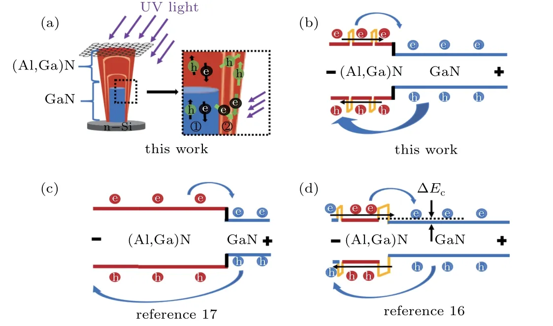
Fig. 5. (a) Schematic diagram of UV irradiation on the photodetector. Enlarged image indicates the diffusion of photogenerated carriers within the core-shell structure. (b)Energy band diagram of the(Al,Ga)N nanowires under UV illumination in this work. (c)Energy band diagram of the(Al,Ga)N nanowires from Ref. [17]. (d) Energy band diagram of the (Al,Ga)N nanowires from Ref.[16].
4. Conclusion
In summary, we demonstrate a dual-wavelength (UVA/UV-C) photodetector based on vertical (Al,Ga)N/GaN nanowires grown by MBE. The current switching characteristics of the detector indicates a good repeatability. Moreover, due to the systematic analysis, the ratio of the thicknesses and the energy band difference of (Al,Ga)N and GaN sections could be the main parameters contributing to the dualwavelength response. By using the transparent graphene, the maximum responsivity of UV-C band is over 15.5 mA·W-1,and the rejection ratio exceeds 35 times at an applied bias of-2 V. This work is pretty promising for promoting the development of dual-wavelength UV detectors for wide applications.
- Chinese Physics B的其它文章
- Numerical simulations of partial elements excitation for hemispherical high-intensity focused ultrasound phased transducer*
- Magnetic-resonance image segmentation based on improved variable weight multi-resolution Markov random field in undecimated complex wavelet domain*
- Structure-based simulations complemented by conventional all-atom simulations to provide new insights into the folding dynamics of human telomeric G-quadruplex*
- Phase-and spin-dependent manipulation of leakage of Majorana mode into double quantum dot*
- Deep-ultraviolet and visible dual-band photodetectors by integrating Chlorin e6 with Ga2O3
- Extended-source broken gate tunnel FET for improving direct current and analog/radio-frequency performance*

